EP1485746B1 - IMPROVED ADDRESSING METHOD OF MOVABLE ELEMENTS IN A SPATIAL LIGHT MODULATOR (slm) - Google Patents
IMPROVED ADDRESSING METHOD OF MOVABLE ELEMENTS IN A SPATIAL LIGHT MODULATOR (slm) Download PDFInfo
- Publication number
- EP1485746B1 EP1485746B1 EP03744576A EP03744576A EP1485746B1 EP 1485746 B1 EP1485746 B1 EP 1485746B1 EP 03744576 A EP03744576 A EP 03744576A EP 03744576 A EP03744576 A EP 03744576A EP 1485746 B1 EP1485746 B1 EP 1485746B1
- Authority
- EP
- European Patent Office
- Prior art keywords
- force
- deflection
- voltage
- movable element
- electrode
- Prior art date
- Legal status (The legal status is an assumption and is not a legal conclusion. Google has not performed a legal analysis and makes no representation as to the accuracy of the status listed.)
- Expired - Lifetime
Links
- 238000000034 method Methods 0.000 title claims abstract description 31
- 230000004044 response Effects 0.000 claims abstract description 15
- 230000005670 electromagnetic radiation Effects 0.000 claims abstract description 13
- 230000009471 action Effects 0.000 claims description 5
- 230000003068 static effect Effects 0.000 claims 2
- 230000003534 oscillatory effect Effects 0.000 claims 1
- 230000000737 periodic effect Effects 0.000 claims 1
- 238000007493 shaping process Methods 0.000 abstract 1
- 239000000463 material Substances 0.000 description 11
- 230000003321 amplification Effects 0.000 description 10
- 238000003199 nucleic acid amplification method Methods 0.000 description 10
- 230000010355 oscillation Effects 0.000 description 10
- 238000013016 damping Methods 0.000 description 9
- 230000001052 transient effect Effects 0.000 description 8
- 239000004020 conductor Substances 0.000 description 6
- 230000001965 increasing effect Effects 0.000 description 4
- 239000000758 substrate Substances 0.000 description 4
- 239000007789 gas Substances 0.000 description 3
- 230000001360 synchronised effect Effects 0.000 description 3
- 230000001133 acceleration Effects 0.000 description 2
- XAGFODPZIPBFFR-UHFFFAOYSA-N aluminium Chemical compound [Al] XAGFODPZIPBFFR-UHFFFAOYSA-N 0.000 description 2
- 229910052782 aluminium Inorganic materials 0.000 description 2
- 230000006399 behavior Effects 0.000 description 2
- 230000008859 change Effects 0.000 description 2
- 230000000694 effects Effects 0.000 description 2
- 230000006870 function Effects 0.000 description 2
- 238000004519 manufacturing process Methods 0.000 description 2
- 238000000059 patterning Methods 0.000 description 2
- 230000005855 radiation Effects 0.000 description 2
- 230000001960 triggered effect Effects 0.000 description 2
- RYGMFSIKBFXOCR-UHFFFAOYSA-N Copper Chemical compound [Cu] RYGMFSIKBFXOCR-UHFFFAOYSA-N 0.000 description 1
- BQCADISMDOOEFD-UHFFFAOYSA-N Silver Chemical compound [Ag] BQCADISMDOOEFD-UHFFFAOYSA-N 0.000 description 1
- 229910045601 alloy Inorganic materials 0.000 description 1
- 239000000956 alloy Substances 0.000 description 1
- 238000005452 bending Methods 0.000 description 1
- 238000005352 clarification Methods 0.000 description 1
- 229910052802 copper Inorganic materials 0.000 description 1
- 239000010949 copper Substances 0.000 description 1
- 230000001419 dependent effect Effects 0.000 description 1
- 238000010586 diagram Methods 0.000 description 1
- 239000013013 elastic material Substances 0.000 description 1
- 230000005684 electric field Effects 0.000 description 1
- 230000002349 favourable effect Effects 0.000 description 1
- PCHJSUWPFVWCPO-UHFFFAOYSA-N gold Chemical compound [Au] PCHJSUWPFVWCPO-UHFFFAOYSA-N 0.000 description 1
- 229910052737 gold Inorganic materials 0.000 description 1
- 239000010931 gold Substances 0.000 description 1
- 238000003384 imaging method Methods 0.000 description 1
- 230000001939 inductive effect Effects 0.000 description 1
- 239000011261 inert gas Substances 0.000 description 1
- 238000001459 lithography Methods 0.000 description 1
- 238000004377 microelectronic Methods 0.000 description 1
- 229910021421 monocrystalline silicon Inorganic materials 0.000 description 1
- 230000003287 optical effect Effects 0.000 description 1
- 238000002310 reflectometry Methods 0.000 description 1
- 230000002441 reversible effect Effects 0.000 description 1
- 239000004065 semiconductor Substances 0.000 description 1
- 229910052709 silver Inorganic materials 0.000 description 1
- 239000004332 silver Substances 0.000 description 1
- 238000009966 trimming Methods 0.000 description 1
- 239000003190 viscoelastic substance Substances 0.000 description 1
Images


Classifications
-
- G—PHYSICS
- G02—OPTICS
- G02B—OPTICAL ELEMENTS, SYSTEMS OR APPARATUS
- G02B26/00—Optical devices or arrangements for the control of light using movable or deformable optical elements
- G02B26/08—Optical devices or arrangements for the control of light using movable or deformable optical elements for controlling the direction of light
- G02B26/0816—Optical devices or arrangements for the control of light using movable or deformable optical elements for controlling the direction of light by means of one or more reflecting elements
- G02B26/0833—Optical devices or arrangements for the control of light using movable or deformable optical elements for controlling the direction of light by means of one or more reflecting elements the reflecting element being a micromechanical device, e.g. a MEMS mirror, DMD
- G02B26/0841—Optical devices or arrangements for the control of light using movable or deformable optical elements for controlling the direction of light by means of one or more reflecting elements the reflecting element being a micromechanical device, e.g. a MEMS mirror, DMD the reflecting element being moved or deformed by electrostatic means
Definitions
- the invention relates to an addressing method of microelements, more particularly, to an addressing method of movable elements in a Spatial Light Modulator (SLM).
- SLM Spatial Light Modulator
- An SLM with an array of actuators used in for example a mask writing tool or a chip manufacturing tool is loaded with a specific pattern, where each actuator is in an addressed state or a non-addressed state before each stamp is printed.
- This pattern may be a subset of the pattern to be printed on the mask or chip respectively.
- Each actuator mirror is deflected electrostatically by applying voltage between the mirror and an underlying address electrode, after which the actuator mirror is allowed to move into it's predetermined deflected state before an electromagnetic radiation source is triggered to print the stamp.
- An addressing method is e.g. known from US 5 382 961 .
- a deflection amplitude of the actuator mirror in a spatial light modulator is determined by a number of factors such an addressing voltage, mirror hinge material stiffness, mirror hinge thickness, electrode to mirror distance etc.
- the addressing voltage is usually the determining free parameter for being able to reach the maximum required mirror deflection amplitude. This, in turn, sets the requirements for a voltage span of an addressing CMOS circuit.
- the addressing voltage will need to increase dramatically for otherwise unchanged parameters.
- a size of a pixel cell in the CMOS circuit is strongly dependent on the voltage span of the addressing CMOS circuit, why for smaller mirror sizes, with increased addressing voltage span, the CMOS circuit becomes the limiting factor for future actuator sizes.
- the invention also relates to an apparatus for creating a pattern as defined in claim 14.
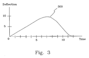
- Figure 3 is a schematic illustration of a deflection versus time curve for a movable microelement when applying a short pulse according to the invention.
- Figure 4b illustrates the applied signal (potential) versus time for the oscillation according to figure 4a .
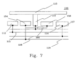
- Figure 7 illustrates a side view of wiring connecting to the mirror structure and electrodes according to another embodiment of the present invention.
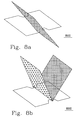
- Figure 8a-8d illustrates the mechanical behavior of a micro mirror element for different orders of resonance frequencies.
- actuators other than deflectable and electrostatic driven micromirrors will be equally applicable; examples are piezoelectric actuators, electrostrictive actuators, piston like actuators of circular or polygonal shape or similar devices.
- Actuating material may be a gap of air, gas, vacuum, viscous, electrostrictive, viscoelastic or elastic material. I t may also be a combination of any of the medias above.
- the movement of the actuator element may be tilting or translational.
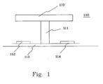
- Figure 1 illustrates schematically a side view of a state of the art actuator structure 100.
- the structure 100 is depicted in an unaddressed state.
- Such an actuator structure 100 may for instance be a micro-mirror structure in a spatial light modulator (SLM).
- the actuator structure depicted in figure 1 , comprises a substrate 113, a first electrode 112 and a second electrode 114, a support structure 111 and a movable element 110.
- Said substrate may be made of semi-conducting material and may comprise one or a plurality of CMOS circuits.
- the first and second electrodes are made of an electrically conductive material, such as gold, copper, silver or alloys of said and/or other electrically conductive materials.
- Said electrodes are connectable to steering circuits, such as the above mentions CMOS circuit.
- the support structure 111 is preferably manufactured of a relatively stiff material, such as single crystal silicon, but may of course be made of materials not having pronounced high stiffness.
- the movable element 110 is preferably manufactured of a material having good optical properties, such as aluminum. However, if a material is selected not having the characteristics as desired, said material may be coated with one or a plurality of layers of other materials having more favorable characteristics, thereby creating a sandwich structure.
- An electrostatic force may deflect the movable element 110. Applying different potentials on the movable element 110 and one of the first 112 and second 113 electrodes creates electrostatic force. In the event of applying a first potential on the movable element 110 and a second potential on said first and second electrodes, where said first and second potentials are different, creates an electrostatic force, but will not deflect said movable element.
- the reason for this is that the attractive force, which force is always attractive independently of the polarity of the potential difference, between the first electrode and the mirror is equivalent to the attractive force between the second potential and the same mirror.
- the two equal attractive forces equalize each other, except of a possible bending of the movable element which is normally very small and can therefore be neglected.
- the actuator structure is illustrated to comprise two electrodes, the first 112 and second 113 electrodes.
- deflecting the movable element requires only one electrode, either the first 112 or second 113 one.
- Figure 2 depicts the actuator structure 100 in an addressed state.
- the actuator structure 100 may be digital, i.e., on-off, or multivalued, i.e., having a plurality of states larger than two.
- one of the first and second electrodes is constantly set to ground potential, the other electrode is set to a variable DC potential and the movable element is set to an AC potential.
- said single electrode is set to said DC potential and the movable element to said AC potential.
- the frequency of the AC potential is chosen to coincide with the mechanical response resonance frequency of a deflecting action of the movable element.
- the resonance frequency for a micro-mirror structure in a spatial light modulator is inter alia determined by the material chosen for the support element 111 and hinge for said mirror. It is also determined by a cross sectional area of the support structure and hinge and the weight of the movable element. We are here talking about the mechanical response resonance frequency of the movable element, not the undesired resonance within the movable element, such as a resonance of curvature of a movable element, which will make the surface of the movable element, such as a micromirror, out-off-flat.
- a pulse of electromagnetic radiation can be synchronized to impinge on the movable element at any state in between maximum or minimum or at said maximum or minimum state.
- said pulse of electromagnetic radiation is synchronized to impinge on said movable element at any of the local maximum or minimum states or at said minimum or maximum state, since for a given time interval, in the order of nanoseconds, the change in deflection is lesser at a maximum or minimum point compared to a point elsewhere on the deflection versus time curve.
- said applied signal is illustrated to be sine-like, however any signal capable to create a mechanical resonance in the movable element is equally applicable.
- the attractive force between the electrode 112, 114 and the movable element 110 is proportional to the square of the difference in potential between said electrode and said element.
- the potential on the movable element 110 is alternating between a max and a min amplitude value in a sinusoidal fashion, and the first and second electrodes 112, 114 or the single electrode is kept at ground potential, the movable element 110 is not deflected, because a frequency of the attractive force is not coinciding with the mechanical resonance frequency as will be described in more detail below.
- the force is, as described above, sin 2 ⁇ ), where ⁇ is the 2 ⁇ f and where f is the frequency of the AC potential. Said frequency f is set to coincide with the mechanical resonance frequency f R of the actuator structure.
- the inventive method for addressing actuators in an SLM may well be used in a pattern generator utilizing an SLM for patterning a workpiece.
- the array may comprise several million micro-mirror structures.
- a state of the art pattern generator for patterning a workpiece using lithography may make use of a pulsed laser source for imaging the pattern on the SLM onto a workpiece. Said stamps of the SLM on said workpiece may constitute only a fraction of the complete pattern to be imaged. Between laser flashes a new pattern description is loaded into the SLM, i.e. individual micromirrors are set to new deflection states by applying a different set of potential differences between the mirror elements and an underlying electrodes.
- a predictive pattern of the SLM can be imaged onto a workpiece.
- a laser may be flashed when the oscillating mirror has reached its maximum deflected state, indicated by 430 in figure 4a , which will require a number of oscillating periods depending mainly on the Q-value of the actuator structure.
- the Q-factor can be determined for a given actuator structure one may synchronize to flash the laser for any amplitude value between a maximum amplitude and a minimum amplitude, for example local maximum points 410, 420 or local minimum points 415, 425.
- all movable elements in a SLM chip are set to the same AC frequency with the same maximum and minimum amplitude values.
- individual movable elements are set to individual maximum and minimum amplitude values and/or individual AC frequency.
- the time i.e., number of periods, it takes for a movable element to come to rest is determined, inter alia, by mechanical losses, ambient material such as any kind of gas including but not limited to air, an inert gas or any type of gas which will improve the behavior of the reflectivity of the movable element being a micromirror, ambient field, e.g., magnetic or electric etc.
- ambient material such as any kind of gas including but not limited to air, an inert gas or any type of gas which will improve the behavior of the reflectivity of the movable element being a micromirror, ambient field, e.g., magnetic or electric etc.
- active cushioning of the resonant frequency said time may be reduced more or less radically.
- Applying a counter AC voltage to the micromirror or at least one electrode out of phase to the one used for amplifying the movement of the movable element may perform active cushioning or damping.
- Applying a magnetic filed around the movable element may also perform damping.
- the cushioning may be enhanced by actively calibrating the required function of the amplitude used for said cushioning.
- the resonance frequency may be adjusted actively.
- the actuator structure depicted in figure 1 may be seen as two coupled oscillating circuits, one mechanical and one electrical.
- the electrical oscillating circuit is defined by a first capacitive circuit between the actuator element and the electrode and an inherent capacitive circuit in steering electronics for said electrodes. Said inherent capacitive circuit may be adjusted actively, thereby trimming the resulting resonance frequency. This may be applied for each individual actuator element separately and independently of each other in an array of actuator elements, such as micro-mirror structures in an SLM.
- the Q value determines the width of the amplifying region for an individual actuator structure.
- a high Q value results in a narrow frequency window with a relatively high amplification factor whereas a low Q value result in a broad frequency window with a relatively low amplification factor.
- Said frequency window should comprise a part which is overlapping for each actuator structure, i.e. by choosing an appropriate design of the actuator element one can optimize the amplification factor given that all actuator element possess an amplification for a given frequency. If a too high amplification is chosen, the width of the frequency window may be too narrow, resulting in non-overlapping amplification regions for different actuator structures.
- the driving voltage can be reduced.
- the Q value is proportional to A*m*(d 2 x/dt 2 )-B*(dx/dt)+C*x, where A, B, C are constants, m is the mass of the movable element, (d 2 x/dt 2 ) is the acceleration of the movable element, (dx/dt) is the velocity of the movable element and x is the spring constant of hinges and support structures attached or attachable to the movable element.
- An ambient material such as its pressure, viscosity and temperature mainly determines the cushioning term, indicated by the minus sign the expression above.
- the gap can be significantly reduced without any risk of "snap-in" by inducing the movement with a force acting only a short time period, for example a time period less than quarter of a period of the microelement resonant oscillation.
- the gap can also be reduced for resonant addressing since an acceleration of the movable element has changed direction when approaching the snap-in state.
- the addressing voltage is applied to one electrode, while the other electrode and the movable element have equal potential.
- the movement will continue after the voltage pulse due to inherent inertia.
- the potential difference between the electrode and the movable element is removed, hence the electric field and therefore the accelerating force is removed. Consequently no "snap-in" can possibly occur.
- the gap can be made only slightly larger than the maximum amplitude of the movement, and the applied voltage can therefore be significantly reduced for a specific addressing voltage.
- said AC potential is constantly applied to said actuator element.
- only a fraction of said AC potential is used, i.e., a pulsed AC potential with a predetermined pulse length.
- a pulsed AC potential with a predetermined pulse length.
- a plurality of signal spikes since a spike comprises a variety of frequencies, inter alia the resonance frequency, an appropriate choice of spike frequency and spike amplitude may set the actuator element into a predetermined and controlled resonance. Most generally a signal is applied which will excite the resonance frequency of the mechanical/electrical system defined by said actuator structure.
- a first ondulating signal is applied to a first electrode 112 and a second ondulating signal is applied to a second electrode 114, where said first and second electrodes 112, 114 belong to the same movable element 110.
- the movable element 110 is addressed with a positive or negative potential.
- Said first and second ondulating signals are arranged to cooperate with each other.
- said first waveform is phase shifted relative to said second waveform.
- said first and second waveforms are out of phase relative to each other by 180 degrees for accomplishing greatest effect.
- Different kinds of waveforms may be applied to the first and second electrodes and other differences in phase than 180 degrees between said first and second ondulating signal may be applicable in order to accomplish greatest effect.
- By applying ondulating signals on two electrodes belonging to the same movable element, which cooperate with each other, may effectively give twice as high attractive force compared to only applying an ondulating signal on the single electrode. This is because the attractive force is alternating between said first and second electrode in cooperative fashion, which doubles the time said attractive force is making a response to said movable element.
- Said first and second electrode 112, 114 are arranged essentially opposite to each other, see figure 1 , which means that the first electrode attract the movable element to deflect in one direction, which is counterclockwise, and the second electrode 114 attract the same movable element 110 to deflect in another direction, which is clockwise.
- the electromagnetic radiation source may be synchronized with the oscillations and for example after a few oscillations it is triggered when the amplitude of the movement is at maximum. By this method, the amplitude of the movement can be amplified by the factor Q for a given fixed addressing voltage.
- one electrode is addressed with a positive or negative potential and a transient pulse is applied to the movable element.
- Said transient pulse is short, i.e., said pulse is switched off before or essentially at the maximum deflection, thereby avoiding said movable element to snap in a maximum deflected state.
- Figure 3 illustrates a deflection of a movable element versus time when applying a 2.5 volt pulse at time 0. Said pulse is switched off after 7 ⁇ s, which is assumed to be the maximum deflection without snap in for this particular actuator structure. The curve can be said to define a ballistic mechanical response.
- the electrode may be addressed with a potential between 0-(-5) V.
- the structure is a movable micromirror, where the movable element (the reflective mirror) has a rectangular shape with sides of 16 ⁇ m, thickness of 1.2 ⁇ m, density of 2.7 g/cm3 and resonance frequency of 460 kHz.
- the micromirror is attached to the support structure 111 by means of springs of aluminum having a length of 5 ⁇ m, a width of 0.6 ⁇ m, a thickness of 0.18 ⁇ m.
- Active damping may reduce the time it takes for said movable element to come to rest. For example, if said transient pulse has been applied to electrode 112 another damping pulse may be applied on electrode 114, or a plurality of pulses applied serially and/or in parallel to both electrodes 112, 114.
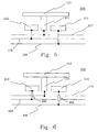
- Figure 5 illustrates a side view of a prior art wiring connecting to the actuator structure 100 comprising a movable modulator microelement 110, first electrode 112 and second electrode 114.
- a first conductor 117 is connected to the movable modulator microelement 110
- a second conductor 115 is connected to the first electrode 112
- a third conductor 116 is connected to the second electrode 114.
- every movable microstructure may be connected to each other or separated to each other, the same applies to said first and second electrodes 112, 114.
- Figure 6 illustrates an inventive embodiment of connecting the electrodes to the wiring.
- a first resistance 162 is connected to the first electrode 112 and a second resistance 164 is connected to the second electrode 114.
- any movement will cause a current to flow through the resistors 162 and 164.
- the dissipated energy is taken from the kinetic energy of the mirror, for example when said mirror is oscillating.
- said movable element will come to rest quicker compared to the prior art wiring diagram because of a resistive damping.
- the resistance can be connectable to any of the electrodes or in separate electrodes as illustrated in figure 7 .
- two extra electrodes 154, 156 functions as damping electrodes.
- Said electrodes are connectable to a conductor 118 via a resistance 160.
- said damping electrodes are arranged closer the support structure 111 than electrodes 112, 114, of course the reverse is applicable or one damping electrode closer to the support structure 112 or 114 on one side and beyond said electrode 114 or 112 on the other side.
- a signal applied causing the movable element to resonate at its resonant frequency is preferably below 1 MHz for a movable element being a micromirror having a square shaped size with sides being approximately 16 ⁇ m.
- the time for setting the movable element in resonance, flashing the electromagnetic radiation at a desired deflection of said movable element, switching off said signal causing said resonance and a settlement to rest of said movable element should preferably be around 20-30 ⁇ s for a flash frequency of the electromagnetic radiation of 8 kHz.
- the amplifying signal and the address signal are applied to the same electrode 112 or 114.
- Said address signal and amplifying signal may be separate signals or a signal belonging to the same waveform.
- said signal which will excite the resonance frequency of said microelements may be switched on a predetermined time period before a beam of electromagnetic radiation impinges onto said SLM.
- Said predetermined time period will allow the microelement to oscillate with determinable amplitude.
- the address signal is in one embodiment of the invention unique for each modulating element with the amplifying signal (short pulse or ondulating signal) equal for all elements.
- a second or higher resonance frequency is superimposed to said first order resonance frequency.
- Said first order resonance frequency will, as described above, coincide with the mechanical response resonance frequency of a deflecting action of the movable element.
- the second or higher orders of resonance frequency will coincide with the mechanical response causing a deflecting action within the movable element.
- Said second or higher orders of resonance frequency may be used to flatten out mirrors, at the exact time of a flash from a writing laser. If the mirrors for some reason are not flat, caused for example from the manufacturing process or due to mechanical stress change over time caused by the radiation from the writing laser, said second or higher orders of resonance frequency may be used to flatten out said non flat mirror.
- a first resonance frequency will be 1.4 MHz
- a second order resonance frequency will be 4.0 MHz
- a third order resonance frequency will be 5.5 MHz
- a fourth order resonance frequency will be 5.7 MHz
- a fifth order resonance frequency will be 11.8 MHz
- a sixth order resonance frequency will be 13.5 MHz.
- FIG 8a-8d illustrates the first, second, third and fourth resonance frequencies respectively for a specific shape of a micro mirror element.
- the whole movable element is tilted around the hinges.
- the movable element will deflect like a butterfly.
- said movable element will be twisted around an axis, which lies in a plane of said movable element and is perpendicular to said hinges.
- the movable element is a combination of a butterfly deflection and a rotation around the same axis as the same movable element is twisted around in figure 8c .
Landscapes
- Physics & Mathematics (AREA)
- General Physics & Mathematics (AREA)
- Optics & Photonics (AREA)
- Mechanical Light Control Or Optical Switches (AREA)
- Control Of Indicators Other Than Cathode Ray Tubes (AREA)
- Micromachines (AREA)
- Liquid Crystal (AREA)
- Mechanical Optical Scanning Systems (AREA)
Applications Claiming Priority (3)
| Application Number | Priority Date | Filing Date | Title |
|---|---|---|---|
| SE0200787 | 2002-03-15 | ||
| SE0200787A SE0200787D0 (sv) | 2002-03-15 | 2002-03-15 | Improved addressing method |
| PCT/SE2003/000427 WO2003079090A1 (en) | 2002-03-15 | 2003-03-14 | IMPROVED ADDRESSING METHOD OF MOVABLE ELEMENTS IN A SPATIAL LIGHT MODULATOR (slm) |
Publications (2)
| Publication Number | Publication Date |
|---|---|
| EP1485746A1 EP1485746A1 (en) | 2004-12-15 |
| EP1485746B1 true EP1485746B1 (en) | 2008-07-30 |
Family
ID=20287276
Family Applications (1)
| Application Number | Title | Priority Date | Filing Date |
|---|---|---|---|
| EP03744576A Expired - Lifetime EP1485746B1 (en) | 2002-03-15 | 2003-03-14 | IMPROVED ADDRESSING METHOD OF MOVABLE ELEMENTS IN A SPATIAL LIGHT MODULATOR (slm) |
Country Status (9)
| Country | Link |
|---|---|
| US (2) | US7075693B2 (enExample) |
| EP (1) | EP1485746B1 (enExample) |
| JP (1) | JP4243546B2 (enExample) |
| CN (1) | CN1324344C (enExample) |
| AT (1) | ATE403175T1 (enExample) |
| AU (1) | AU2003215999A1 (enExample) |
| DE (1) | DE60322517D1 (enExample) |
| SE (1) | SE0200787D0 (enExample) |
| WO (1) | WO2003079090A1 (enExample) |
Families Citing this family (28)
| Publication number | Priority date | Publication date | Assignee | Title |
|---|---|---|---|---|
| SE0100336L (sv) | 2001-02-05 | 2002-08-06 | Micronic Laser Systems Ab | Adresseringsmetod och apparat som använder densamma tekniskt område |
| US7410736B2 (en) | 2003-09-30 | 2008-08-12 | Asml Holding N.V. | Methods and systems to compensate for a stitching disturbance of a printed pattern in a maskless lithography system not utilizing overlap of the exposure zones |
| US6876440B1 (en) | 2003-09-30 | 2005-04-05 | Asml Holding N.V. | Methods and systems to compensate for a stitching disturbance of a printed pattern in a maskless lithography system utilizing overlap of exposure zones with attenuation of the aerial image in the overlap region |
| US7023526B2 (en) | 2003-09-30 | 2006-04-04 | Asml Holding N.V. | Methods and systems to compensate for a stitching disturbance of a printed pattern in a maskless lithography system utilizing overlap without an explicit attenuation |
| US7839561B2 (en) * | 2007-02-26 | 2010-11-23 | Silicon Quest Kabushiki-Kaisha | Micromirror device with a single address electrode |
| US20090033878A1 (en) * | 2003-11-01 | 2009-02-05 | Akira Shirai | System configurations and methods for controlling image projection apparatuses and mirror device |
| US7336290B2 (en) | 2004-01-07 | 2008-02-26 | Texas Instruments Incorporated | Method and apparatus for increasing a perceived resolution of a display |
| JP4073886B2 (ja) * | 2004-03-30 | 2008-04-09 | アンリツ株式会社 | 可変波長光源 |
| US7072090B2 (en) * | 2004-04-22 | 2006-07-04 | Micronic Laser Systems Ab | Addressing of an SLM |
| US7499146B2 (en) * | 2005-03-14 | 2009-03-03 | Asml Netherlands B.V. | Lithographic apparatus and device manufacturing method, an integrated circuit, a flat panel display, and a method of compensating for cupping |
| US7372617B2 (en) * | 2005-07-06 | 2008-05-13 | Peter Enoksson | Hidden hinge MEMS device |
| JP2007033787A (ja) * | 2005-07-26 | 2007-02-08 | Fujifilm Corp | 微小薄膜可動素子および微小薄膜可動素子アレイ並びに微小薄膜可動素子アレイの駆動方法 |
| US7443568B2 (en) * | 2006-05-04 | 2008-10-28 | Miradia Inc. | Method and system for resonant operation of a reflective spatial light modulator |
| US7505195B2 (en) | 2006-05-04 | 2009-03-17 | Miradia Inc. | Reflective spatial light modulator with high stiffness torsion spring hinge |
| US20080231936A1 (en) * | 2007-03-02 | 2008-09-25 | Taro Endo | Display system comprising a mirror device with micromirrors controlled to operate in intermediate oscillating state |
| US7961161B2 (en) * | 2007-03-02 | 2011-06-14 | Silicon Quest Kabushiki-Kaisha | Display system comprising a mirror device with micromirrors controlled to operate in intermediate oscillating state |
| US9250536B2 (en) | 2007-03-30 | 2016-02-02 | Asml Netherlands B.V. | Lithographic apparatus and method |
| US8937706B2 (en) * | 2007-03-30 | 2015-01-20 | Asml Netherlands B.V. | Lithographic apparatus and method |
| JP5239594B2 (ja) * | 2008-07-30 | 2013-07-17 | 富士通株式会社 | クリップ検出装置及び方法 |
| US8861066B2 (en) | 2009-02-16 | 2014-10-14 | Micronic Ab | Oversized micro-mechanical light modulator with redundant elements, device and method |
| NL2006625A (en) * | 2010-05-26 | 2011-11-29 | Asml Netherlands Bv | Illumination system and lithographic apparatus. |
| DE102011081042B4 (de) * | 2011-08-16 | 2021-05-27 | Robert Bosch Gmbh | Steuervorrichtung für einen Mikrospiegel, Verfahren zum Ansteuern eines Mikrospiegels und Bildprojektionssystem |
| CN102354050B (zh) * | 2011-09-28 | 2013-01-02 | 哈尔滨工业大学 | 柔性辅助臂跟随超高角灵敏度高频响微角摆控制反射镜 |
| US20130286463A1 (en) * | 2011-10-24 | 2013-10-31 | Texas Instruments Incorporated | Dynamic actuation waveform for a digital micromirror device |
| FR2985320B1 (fr) * | 2011-12-29 | 2014-02-14 | Alpao | Systeme a etalonnage commun et procede correspondant |
| DE102015205404A1 (de) * | 2015-03-25 | 2016-09-29 | Carl Zeiss Smt Gmbh | Vielspiegel-Anordnung |
| CN109557661B (zh) * | 2018-10-15 | 2021-02-26 | 武汉光迅科技股份有限公司 | 驱动光学转镜转动的方法及用于驱动光学转镜转动的装置 |
| CN111552072B (zh) * | 2020-04-28 | 2022-07-12 | 安徽中科米微电子技术有限公司 | 大尺寸mems垂直梳齿微镜及其制备方法 |
Family Cites Families (16)
| Publication number | Priority date | Publication date | Assignee | Title |
|---|---|---|---|---|
| US5032924A (en) * | 1989-04-10 | 1991-07-16 | Nilford Laboratories, Inc. | System for producing an image from a sequence of pixels |
| US5285196A (en) * | 1992-10-15 | 1994-02-08 | Texas Instruments Incorporated | Bistable DMD addressing method |
| US5526172A (en) * | 1993-07-27 | 1996-06-11 | Texas Instruments Incorporated | Microminiature, monolithic, variable electrical signal processor and apparatus including same |
| US5488862A (en) * | 1993-10-18 | 1996-02-06 | Armand P. Neukermans | Monolithic silicon rate-gyro with integrated sensors |
| US6044705A (en) * | 1993-10-18 | 2000-04-04 | Xros, Inc. | Micromachined members coupled for relative rotation by torsion bars |
| US5949570A (en) * | 1995-06-20 | 1999-09-07 | Matsushita Electric Industrial Co., Ltd. | Diffractive optical modulator and method for producing the same, infrared sensor including such a diffractive optical modulator and method for producing the same, and display device including such a diffractive optical modulator |
| US5771116A (en) | 1996-10-21 | 1998-06-23 | Texas Instruments Incorporated | Multiple bias level reset waveform for enhanced DMD control |
| US6323982B1 (en) * | 1998-05-22 | 2001-11-27 | Texas Instruments Incorporated | Yield superstructure for digital micromirror device |
| KR100311032B1 (ko) * | 1999-10-29 | 2001-11-02 | 윤종용 | 마이크로미러 가동장치 |
| JP2001228552A (ja) * | 2000-02-17 | 2001-08-24 | Fuji Photo Film Co Ltd | プリンタ |
| US6600591B2 (en) * | 2001-06-12 | 2003-07-29 | Network Photonics, Inc. | Micromirror array having adjustable mirror angles |
| US7190509B2 (en) * | 2001-11-07 | 2007-03-13 | Trex Enterprises Corp. | Optically addressed MEMS |
| US6757092B2 (en) * | 2001-12-10 | 2004-06-29 | Nayef M. Abu-Ageel | Micro-machine electrostatic actuator, method and system employing same, and fabrication methods thereof |
| KR100630029B1 (ko) * | 2002-11-06 | 2006-09-27 | 마츠시타 덴끼 산교 가부시키가이샤 | 변위 검출 기능을 구비한 마이크로 액츄에이터, 및 당해마이크로 액츄에이터를 구비한 가변형 미러 |
| US6956683B2 (en) * | 2003-06-11 | 2005-10-18 | Texas Instruments Incorporated | Pivoting platform having a piezoelectric drive |
| US20070132681A1 (en) * | 2005-12-09 | 2007-06-14 | Chih-Liang Chen | Passive micro-mirror-array spatial light modulation |
-
2002
- 2002-03-15 SE SE0200787A patent/SE0200787D0/xx unknown
-
2003
- 2003-03-14 WO PCT/SE2003/000427 patent/WO2003079090A1/en not_active Ceased
- 2003-03-14 AT AT03744576T patent/ATE403175T1/de not_active IP Right Cessation
- 2003-03-14 DE DE60322517T patent/DE60322517D1/de not_active Expired - Lifetime
- 2003-03-14 EP EP03744576A patent/EP1485746B1/en not_active Expired - Lifetime
- 2003-03-14 AU AU2003215999A patent/AU2003215999A1/en not_active Abandoned
- 2003-03-14 JP JP2003577037A patent/JP4243546B2/ja not_active Expired - Fee Related
- 2003-03-14 US US10/507,554 patent/US7075693B2/en not_active Expired - Fee Related
- 2003-03-14 CN CNB038061686A patent/CN1324344C/zh not_active Expired - Fee Related
-
2006
- 2006-04-14 US US11/404,340 patent/US20060187517A1/en not_active Abandoned
Also Published As
| Publication number | Publication date |
|---|---|
| ATE403175T1 (de) | 2008-08-15 |
| WO2003079090A1 (en) | 2003-09-25 |
| US20050122558A1 (en) | 2005-06-09 |
| CN1324344C (zh) | 2007-07-04 |
| SE0200787D0 (sv) | 2002-03-15 |
| AU2003215999A1 (en) | 2003-09-29 |
| DE60322517D1 (de) | 2008-09-11 |
| US20060187517A1 (en) | 2006-08-24 |
| US7075693B2 (en) | 2006-07-11 |
| EP1485746A1 (en) | 2004-12-15 |
| JP4243546B2 (ja) | 2009-03-25 |
| JP2005521078A (ja) | 2005-07-14 |
| CN1643432A (zh) | 2005-07-20 |
Similar Documents
| Publication | Publication Date | Title |
|---|---|---|
| EP1485746B1 (en) | IMPROVED ADDRESSING METHOD OF MOVABLE ELEMENTS IN A SPATIAL LIGHT MODULATOR (slm) | |
| JP2005521078A5 (enExample) | ||
| KR101284542B1 (ko) | 반발 모드 작동식 주사 미세 거울 | |
| US6758983B2 (en) | Staggered torsional electrostatic combdrive and method of forming same | |
| JP4405555B2 (ja) | 光学ピクセルデバイス | |
| US20050156481A1 (en) | Optical scanning using vibratory diffraction gratings | |
| Tani et al. | A two-axis piezoelectric tilting micromirror with a newly developed PZT-meandering actuator | |
| EP3164755B1 (en) | Micro-optical electromechanical device and method for manufacturing it | |
| US8853804B2 (en) | Tilting actuator with close-gap electrodes | |
| JP3759598B2 (ja) | アクチュエータ | |
| JP2008020701A (ja) | 2次元光スキャナ、それを用いた光学装置および2次元光スキャナの製造方法 | |
| JP2011064928A (ja) | 2次元光スキャナ | |
| US20220127136A1 (en) | Mems actuator and mems actuator array with a plurality of mems actuators | |
| JP5049904B2 (ja) | 可動構造体及びそれを用いた光走査ミラー | |
| WO2002059942A2 (en) | Actuator and micromirror for fast beam steering and method of fabricating the same | |
| TWI467231B (zh) | 操作微鏡陣列之方法 | |
| US20050195400A1 (en) | Fabre-perot interferometer | |
| Bifano et al. | Micromachined deformable mirror for optical wavefront compensation | |
| Tsaur et al. | 2D micro scanner actuated by sol-gel derived double layered PZT | |
| Davis et al. | High-performance silicon scanning mirror for laser printing | |
| WO2003079091A1 (en) | An adressing method of moveable microelements in a spatial light modulator (slm) for pattering of a workpiece | |
| EP0548831B1 (en) | Resonant mirror and method of manufacture | |
| Sasaki et al. | Two-Dimensional Piezoelectrically Actuated Micromirror with Fast Focusing Function | |
| KR100719102B1 (ko) | 마이크로 구동 장치 | |
| KR100677204B1 (ko) | 2축 회전이 가능한 마이크로미러 |
Legal Events
| Date | Code | Title | Description |
|---|---|---|---|
| PUAI | Public reference made under article 153(3) epc to a published international application that has entered the european phase |
Free format text: ORIGINAL CODE: 0009012 |
|
| 17P | Request for examination filed |
Effective date: 20040818 |
|
| AK | Designated contracting states |
Kind code of ref document: A1 Designated state(s): AT BE BG CH CY CZ DE DK EE ES FI FR GB GR HU IE IT LI LU MC NL PT RO SE SI SK TR |
|
| AX | Request for extension of the european patent |
Extension state: AL LT LV MK |
|
| 17Q | First examination report despatched |
Effective date: 20061207 |
|
| GRAP | Despatch of communication of intention to grant a patent |
Free format text: ORIGINAL CODE: EPIDOSNIGR1 |
|
| GRAS | Grant fee paid |
Free format text: ORIGINAL CODE: EPIDOSNIGR3 |
|
| GRAA | (expected) grant |
Free format text: ORIGINAL CODE: 0009210 |
|
| AK | Designated contracting states |
Kind code of ref document: B1 Designated state(s): AT BE BG CH CY CZ DE DK EE ES FI FR GB GR HU IE IT LI LU MC NL PT RO SE SI SK TR |
|
| REG | Reference to a national code |
Ref country code: GB Ref legal event code: FG4D |
|
| REG | Reference to a national code |
Ref country code: CH Ref legal event code: EP |
|
| REF | Corresponds to: |
Ref document number: 60322517 Country of ref document: DE Date of ref document: 20080911 Kind code of ref document: P |
|
| REG | Reference to a national code |
Ref country code: IE Ref legal event code: FG4D |
|
| REG | Reference to a national code |
Ref country code: SE Ref legal event code: TRGR |
|
| PG25 | Lapsed in a contracting state [announced via postgrant information from national office to epo] |
Ref country code: PT Free format text: LAPSE BECAUSE OF FAILURE TO SUBMIT A TRANSLATION OF THE DESCRIPTION OR TO PAY THE FEE WITHIN THE PRESCRIBED TIME-LIMIT Effective date: 20081230 Ref country code: ES Free format text: LAPSE BECAUSE OF FAILURE TO SUBMIT A TRANSLATION OF THE DESCRIPTION OR TO PAY THE FEE WITHIN THE PRESCRIBED TIME-LIMIT Effective date: 20081110 |
|
| PG25 | Lapsed in a contracting state [announced via postgrant information from national office to epo] |
Ref country code: SI Free format text: LAPSE BECAUSE OF FAILURE TO SUBMIT A TRANSLATION OF THE DESCRIPTION OR TO PAY THE FEE WITHIN THE PRESCRIBED TIME-LIMIT Effective date: 20080730 Ref country code: BG Free format text: LAPSE BECAUSE OF FAILURE TO SUBMIT A TRANSLATION OF THE DESCRIPTION OR TO PAY THE FEE WITHIN THE PRESCRIBED TIME-LIMIT Effective date: 20081030 Ref country code: FI Free format text: LAPSE BECAUSE OF FAILURE TO SUBMIT A TRANSLATION OF THE DESCRIPTION OR TO PAY THE FEE WITHIN THE PRESCRIBED TIME-LIMIT Effective date: 20080730 Ref country code: AT Free format text: LAPSE BECAUSE OF FAILURE TO SUBMIT A TRANSLATION OF THE DESCRIPTION OR TO PAY THE FEE WITHIN THE PRESCRIBED TIME-LIMIT Effective date: 20080730 |
|
| PG25 | Lapsed in a contracting state [announced via postgrant information from national office to epo] |
Ref country code: BE Free format text: LAPSE BECAUSE OF FAILURE TO SUBMIT A TRANSLATION OF THE DESCRIPTION OR TO PAY THE FEE WITHIN THE PRESCRIBED TIME-LIMIT Effective date: 20080730 |
|
| PG25 | Lapsed in a contracting state [announced via postgrant information from national office to epo] |
Ref country code: DK Free format text: LAPSE BECAUSE OF FAILURE TO SUBMIT A TRANSLATION OF THE DESCRIPTION OR TO PAY THE FEE WITHIN THE PRESCRIBED TIME-LIMIT Effective date: 20080730 Ref country code: EE Free format text: LAPSE BECAUSE OF FAILURE TO SUBMIT A TRANSLATION OF THE DESCRIPTION OR TO PAY THE FEE WITHIN THE PRESCRIBED TIME-LIMIT Effective date: 20080730 |
|
| PG25 | Lapsed in a contracting state [announced via postgrant information from national office to epo] |
Ref country code: SK Free format text: LAPSE BECAUSE OF FAILURE TO SUBMIT A TRANSLATION OF THE DESCRIPTION OR TO PAY THE FEE WITHIN THE PRESCRIBED TIME-LIMIT Effective date: 20080730 Ref country code: RO Free format text: LAPSE BECAUSE OF FAILURE TO SUBMIT A TRANSLATION OF THE DESCRIPTION OR TO PAY THE FEE WITHIN THE PRESCRIBED TIME-LIMIT Effective date: 20080730 Ref country code: CZ Free format text: LAPSE BECAUSE OF FAILURE TO SUBMIT A TRANSLATION OF THE DESCRIPTION OR TO PAY THE FEE WITHIN THE PRESCRIBED TIME-LIMIT Effective date: 20080730 |
|
| PLBE | No opposition filed within time limit |
Free format text: ORIGINAL CODE: 0009261 |
|
| STAA | Information on the status of an ep patent application or granted ep patent |
Free format text: STATUS: NO OPPOSITION FILED WITHIN TIME LIMIT |
|
| 26N | No opposition filed |
Effective date: 20090506 |
|
| PG25 | Lapsed in a contracting state [announced via postgrant information from national office to epo] |
Ref country code: IT Free format text: LAPSE BECAUSE OF FAILURE TO SUBMIT A TRANSLATION OF THE DESCRIPTION OR TO PAY THE FEE WITHIN THE PRESCRIBED TIME-LIMIT Effective date: 20080730 |
|
| PGFP | Annual fee paid to national office [announced via postgrant information from national office to epo] |
Ref country code: SE Payment date: 20090317 Year of fee payment: 7 |
|
| PG25 | Lapsed in a contracting state [announced via postgrant information from national office to epo] |
Ref country code: MC Free format text: LAPSE BECAUSE OF NON-PAYMENT OF DUE FEES Effective date: 20090331 |
|
| REG | Reference to a national code |
Ref country code: CH Ref legal event code: PL |
|
| REG | Reference to a national code |
Ref country code: FR Ref legal event code: ST Effective date: 20091130 |
|
| PG25 | Lapsed in a contracting state [announced via postgrant information from national office to epo] |
Ref country code: IE Free format text: LAPSE BECAUSE OF NON-PAYMENT OF DUE FEES Effective date: 20090314 Ref country code: CH Free format text: LAPSE BECAUSE OF NON-PAYMENT OF DUE FEES Effective date: 20090331 Ref country code: LI Free format text: LAPSE BECAUSE OF NON-PAYMENT OF DUE FEES Effective date: 20090331 |
|
| PG25 | Lapsed in a contracting state [announced via postgrant information from national office to epo] |
Ref country code: FR Free format text: LAPSE BECAUSE OF NON-PAYMENT OF DUE FEES Effective date: 20091123 |
|
| PG25 | Lapsed in a contracting state [announced via postgrant information from national office to epo] |
Ref country code: GR Free format text: LAPSE BECAUSE OF FAILURE TO SUBMIT A TRANSLATION OF THE DESCRIPTION OR TO PAY THE FEE WITHIN THE PRESCRIBED TIME-LIMIT Effective date: 20081031 |
|
| EUG | Se: european patent has lapsed | ||
| PG25 | Lapsed in a contracting state [announced via postgrant information from national office to epo] |
Ref country code: LU Free format text: LAPSE BECAUSE OF NON-PAYMENT OF DUE FEES Effective date: 20090314 |
|
| PG25 | Lapsed in a contracting state [announced via postgrant information from national office to epo] |
Ref country code: HU Free format text: LAPSE BECAUSE OF FAILURE TO SUBMIT A TRANSLATION OF THE DESCRIPTION OR TO PAY THE FEE WITHIN THE PRESCRIBED TIME-LIMIT Effective date: 20090131 |
|
| PGFP | Annual fee paid to national office [announced via postgrant information from national office to epo] |
Ref country code: GB Payment date: 20110325 Year of fee payment: 9 |
|
| PG25 | Lapsed in a contracting state [announced via postgrant information from national office to epo] |
Ref country code: TR Free format text: LAPSE BECAUSE OF FAILURE TO SUBMIT A TRANSLATION OF THE DESCRIPTION OR TO PAY THE FEE WITHIN THE PRESCRIBED TIME-LIMIT Effective date: 20080730 |
|
| PG25 | Lapsed in a contracting state [announced via postgrant information from national office to epo] |
Ref country code: CY Free format text: LAPSE BECAUSE OF FAILURE TO SUBMIT A TRANSLATION OF THE DESCRIPTION OR TO PAY THE FEE WITHIN THE PRESCRIBED TIME-LIMIT Effective date: 20080730 |
|
| PG25 | Lapsed in a contracting state [announced via postgrant information from national office to epo] |
Ref country code: SE Free format text: LAPSE BECAUSE OF NON-PAYMENT OF DUE FEES Effective date: 20100315 |
|
| GBPC | Gb: european patent ceased through non-payment of renewal fee |
Effective date: 20120314 |
|
| PG25 | Lapsed in a contracting state [announced via postgrant information from national office to epo] |
Ref country code: GB Free format text: LAPSE BECAUSE OF NON-PAYMENT OF DUE FEES Effective date: 20120314 |
|
| PGFP | Annual fee paid to national office [announced via postgrant information from national office to epo] |
Ref country code: DE Payment date: 20150327 Year of fee payment: 13 Ref country code: NL Payment date: 20150326 Year of fee payment: 13 |
|
| REG | Reference to a national code |
Ref country code: DE Ref legal event code: R119 Ref document number: 60322517 Country of ref document: DE |
|
| REG | Reference to a national code |
Ref country code: NL Ref legal event code: MM Effective date: 20160401 |
|
| PG25 | Lapsed in a contracting state [announced via postgrant information from national office to epo] |
Ref country code: DE Free format text: LAPSE BECAUSE OF NON-PAYMENT OF DUE FEES Effective date: 20161001 Ref country code: NL Free format text: LAPSE BECAUSE OF NON-PAYMENT OF DUE FEES Effective date: 20160401 |