EP1476875B1 - Mram ohne isolationseinrichtungen - Google Patents
Mram ohne isolationseinrichtungen Download PDFInfo
- Publication number
- EP1476875B1 EP1476875B1 EP03731902A EP03731902A EP1476875B1 EP 1476875 B1 EP1476875 B1 EP 1476875B1 EP 03731902 A EP03731902 A EP 03731902A EP 03731902 A EP03731902 A EP 03731902A EP 1476875 B1 EP1476875 B1 EP 1476875B1
- Authority
- EP
- European Patent Office
- Prior art keywords
- data
- column
- current
- magnetoresistive elements
- bitline
- Prior art date
- Legal status (The legal status is an assumption and is not a legal conclusion. Google has not performed a legal analysis and makes no representation as to the accuracy of the status listed.)
- Expired - Lifetime
Links
- 238000002955 isolation Methods 0.000 title claims abstract description 39
- 230000008878 coupling Effects 0.000 claims 2
- 238000010168 coupling process Methods 0.000 claims 2
- 238000005859 coupling reaction Methods 0.000 claims 2
- 230000015654 memory Effects 0.000 description 34
- 238000010586 diagram Methods 0.000 description 18
- 239000013598 vector Substances 0.000 description 7
- 238000004519 manufacturing process Methods 0.000 description 5
- 238000000034 method Methods 0.000 description 5
- 230000003213 activating effect Effects 0.000 description 3
- 238000003491 array Methods 0.000 description 3
- 230000005415 magnetization Effects 0.000 description 3
- 238000010276 construction Methods 0.000 description 2
- 239000000463 material Substances 0.000 description 2
- 238000012986 modification Methods 0.000 description 2
- 230000004048 modification Effects 0.000 description 2
- 239000004065 semiconductor Substances 0.000 description 2
- 239000000758 substrate Substances 0.000 description 2
- 230000015556 catabolic process Effects 0.000 description 1
- 238000006731 degradation reaction Methods 0.000 description 1
- 230000006870 function Effects 0.000 description 1
- 239000010409 thin film Substances 0.000 description 1
- 230000005641 tunneling Effects 0.000 description 1
Images



Classifications
-
- G—PHYSICS
- G11—INFORMATION STORAGE
- G11C—STATIC STORES
- G11C7/00—Arrangements for writing information into, or reading information out from, a digital store
- G11C7/14—Dummy cell management; Sense reference voltage generators
-
- G—PHYSICS
- G11—INFORMATION STORAGE
- G11C—STATIC STORES
- G11C11/00—Digital stores characterised by the use of particular electric or magnetic storage elements; Storage elements therefor
- G11C11/02—Digital stores characterised by the use of particular electric or magnetic storage elements; Storage elements therefor using magnetic elements
- G11C11/14—Digital stores characterised by the use of particular electric or magnetic storage elements; Storage elements therefor using magnetic elements using thin-film elements
- G11C11/15—Digital stores characterised by the use of particular electric or magnetic storage elements; Storage elements therefor using magnetic elements using thin-film elements using multiple magnetic layers
-
- G—PHYSICS
- G11—INFORMATION STORAGE
- G11C—STATIC STORES
- G11C11/00—Digital stores characterised by the use of particular electric or magnetic storage elements; Storage elements therefor
- G11C11/02—Digital stores characterised by the use of particular electric or magnetic storage elements; Storage elements therefor using magnetic elements
- G11C11/16—Digital stores characterised by the use of particular electric or magnetic storage elements; Storage elements therefor using magnetic elements using elements in which the storage effect is based on magnetic spin effect
- G11C11/165—Auxiliary circuits
- G11C11/1673—Reading or sensing circuits or methods
Definitions
- This invention relates to magnetoresistive memories and more particularly, to MRAM array architecture designed so that isolation devices are not required.
- MRAMs Thin film Magnetoresistive Random Access Memories
- MTJ Magnetic Tunneling Junction
- the MTJ cell essentially consists of a pair of magnetic layers with an insulating layer sandwiched therebetween.
- One of the magnetic layers has a fixed magnetic vector and the other magnetic layer has a changeable magnetic vector that is either aligned with or opposed to the fixed magnetic vector.
- the resistance of the MTJ cell i.e. the resistance to current flow between the magnetic layers, is a minimum and when the magnetic vectors are opposed or misaligned the resistance of the MTJ cell is a maximum.
- Data is stored in the MTJ cell by applying a magnetic field to the MTJ cell directed so as to move the changeable magnetic vector to a selected orientation.
- the aligned orientation can be designated a logic 1 or 0 and the misaligned orientation is the opposite, i.e. a logic 0 or 1.
- Stored data is read or sensed by passing a current through the MTJ cell from one magnetic layer to the other. The amount of current passing through the MTJ cell, or voltage drop across the MTJ cell, will vary according to the orientation of the changeable magnetic vector. Additional information as to the fabrication and operation of the MTJ memory cells can be found in Patent No: 5, 702,831, entitled “Multi-Layer Magnetic Tunnelling Junction Memory Cells", issued 31 March 1998.
- an isolation device generally a transistor in series or in parallel with each magnetoresistive device in a memory array, is included to avoid leakage paths throughout memory array.
- the magnetoresistive device and the isolation device are fabricated as a single unit.
- an isolation transistor is usually fabricated on a semiconductor substrate and the associated magnetoresistive device is fabricated on the isolation magnetoresistive device is fabricated on the isolation transistor so as to be connected internally.
- One of the problems in this structure is the amount of manufacturing effort required to produce the combined isolation transistor and magnetoresistive device and the control lines required for operation. Also, the large number of isolation devices and control lines for the isolation devices substantially increases the size of the memory array.
- magnetoresistive devices without isolation devices are connected so that one input of a differential amplifier is connected to a target column containing the Magnetoresistive device being read, with the other input connected to ground. Feedback within the differential amplifier clamps the target column to a ground potential. All other columns in the array are grounded (i.e. the bitlines are clamped to ground) by means of column select transistors.
- the read process is performed by applying a read voltage to the row containing the Magnetoresistive device to be read and to all other magnetoresistive devices in the row. Supposedly, since all columns in the array are at ground potential, no current flows between the magnetoresistive device not being read on deselected rows.
- a major problem with this architecture is that it fails to equalize target (column being read) and other columns adequately, due to non-idealization of clamp circuits, resulting in sneak paths which yield signal loss and speed degradation.
- a target column and an associated reference column are connected through a sense amplifier to an output terminal.
- the sense amplifier sources bitline current through the target column and the references column and clamps the two columns to the same potential. Changes in the current in the target cell (in the target column) are compared with current through the reference cells (in the reference column).
- target and reference columns will not clamp to exactly the same voltage, resulting in sneak paths.
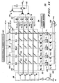
- FIG. 1 a simplified schematic diagram is illustrated of an isolation free magnetoresistive memory array 10 with an interspersed reference column 12 in accordance with the present invention.
- array 10 is a 4x4 array and reference column 12 includes two midpoint generators 14 and 15 with each generator 14 and 15 taking up two rows of magnetoresistive elements.
- a plurality of non-volatile magnetoresistive elements (each designated 13), each programmable to one of an Rmax and an Rmin state, are connected to have information stored therein.
- the non-volatile magnetoresistive elements 13 in a data column e.g.
- column BL 0 are each directly connected, without incorporating isolation devices, at one end to the column bitline BL 0 and at the other end to a digitline of a plurality of digit lines DL 0 through DL 3 .
- Each bitline, BL 0 through BL 3 and BLref, is connected to output terminals Vo 0 through Vo 3 and Voref, respectively, through current conveyor circuits 16 through 20.
- FIG. 2 a simplified block diagram is illustrated of an embodiment of current conveyor circuit 16 as used in the readout portion of array 10 of FIG. 1. Since each of the current conveyor circuits 16 through 20 is similar, only circuit 16 will be described in detail.
- the block diagram of circuit 16 is illustrated primarily to describe the construction and operation of the current conveyors in conjunction with an array, such as array 10.
- any one, or all, of the current conveyors 16 through 20, or any other current conveyors described or referred to below may constitute a current sensor, current amplifier, preamplifier, current source, clamp circuit. current to voltage converter, etc. or any combination of the above that performs the intended and described purpose, and will be hereinafter referred to simply as a "current conveyor” or "current conveyor circuit”.
- current conveyor 16 includes a low impedance terminal circuit 21 having a terminal connected to bitline BL 0 to receive I BL bitline current.
- a V BIAS signal is also applied to circuit 21 to provide a clamping reference.
- a second terminal of circuit 21 takes a portion of the current from a current source 23 applied to an input of a high impedance input circuit 22.
- Circuit 21 conveys a portion of the current from current source 23 from one terminal to the other.
- Circuit 22 converts the current to an output voltage V o0 .
- circuit 21 can include a clamp circuit, a current sensor, a current sense amplifier, a pre-amplifier or the like.
- Circuit 22 can include a converter, an amplifier, a second sense amplifier, or the like and is generally included to essentially provide current mode operation.
- Current conveyor 16 has a very low input impedance, isolating bitline BL 0 from the high output impedance of current source 23. The low input impedance combined with the clamping of BL 0 limits the voltage swing of bitline BL 0 and achieves high speed readout for very high density MTJ arrays. Thus, current conveyor 16 provides and maintains a constant bias across bitline Bl 0 regardless of operating temperatures, changes in the supply voltage, and process conditions. Also, current conveyor 16 provides a small swing in the voltage on bitline BL 0 to allow for high speed operation.
- circuit 20 includes a similar pair of current conveyor connected to bitline BLref, which serves as a reference column in array 10.
- bitline BLref which serves as a reference column in array 10.
- FIG. 3 illustrates a simplified schematic diagram showing the operation of a midpoint generator 40.
- a midpoint resistance midway, or half way, between Rmin and Rmax is designated Rmid.
- Equation (1) is implemented by a series/parallel combination of magnetoresistive elements as illustrated in FIG. 3. Magnetoresistive elements can be combined in this manner because they are linear elements to the first order and, therefore, they can be treated as ordinary passive linear resistors.
- midpoint generator 40 includes an input terminal 41 and an output terminal 42.
- a series circuit 44 includes a magnetoresistive element 45, with a resistance equal to Rmax, connected in series with a magnetoresistive element 46, with a resistance equal to Rmin, connected in series between input terminal 41 and output terminal 42.
- Another series circuit 47 includes a magnetoresistive element 48, with a resistance equal to Rmax, connected in series with a magnetoresistive element 49, with a resistance equal to Rmin, connected in series between input terminal 41 and output terminal 42.
- Series circuit 44 is also connected in parallel with series circuit 47 to form the series/parallel combination.
- R AB Rmax + Rmin 2 / 2 ⁇
- R AB ⁇ R / 2 + Rmin
- equation (2) is equal to equation (1), i.e. R AB is equal to Rmid, and generator 40 successfully generates the midpoint Rmid.
- magnetoresistive elements are non-volatile memory elements which can be programmed into an Rmax or an Rmin state, where Rmin is a minimum resistive value corresponding to parallel states of magnetization and Rmax is a maximum resistive value corresponding to anti-parallel states of magnetization.
- magnetoresistive elements are generally initially in the Rmin state and must be programmed into the Rmax state prior to the generation of Rmid. This programming can be done as a one time effort and, thereafter, Rmax is generated automatically without any need to reprogram, since the magnetoresistive elements hold their magnetization state in a non volatile fashion.
- a schematic diagram is illustrated, for example only, of midpoint generator 14, to show current flow during a readout operation.
- every two digit lines have an associated digit reference line (e.g. DL 0 and DL 1 are associated with DL ref ). Further, if either of the two digit lines is selected (e.g. either DL 0 and DL 1 ), the associated digit reference line (i.e. DL ref ) will be selected also.
- a selected digit line is grounded along with its associated digit reference line. In the example illustrated in FIG. 4, digit reference line DL ref0 is grounded.
- Midpoint generator 14 includes magnetoresistive elements 52 through 55.
- midpoint generator 14 is basically the same as the structure of FIG. 3 with bitline BL ref acting as one output terminal and digitline DL ref acting as the other output terminal with the resistance between the output terminals being the midpoint Rmid.
- FIG. 1 a new architecture for a magnetoresistive memory array free of isolation devices is illustrated in FIG. 1.
- current conveyors 16 through 20 source current through bitlines BL 0 through BL 1 and BL ref , respectively. Also, since all current conveyors 16 through 20 are identical and since all columns, including the reference columns, are identical, current conveyors 16 through 20 clamp bitlines BL 0 through BL 1 and BL ref to identical voltages. The clamping voltages of all columns or bitlines are identical (or very close), thereby minimizing column-to-column leakage.
- Isolation free magnetoresistive memory array 10 would not operate as described without midpoint generators 14 and 15, since to be able to distinguish between Rmin and Rmax the reference column would have to be clamped to a different voltage or an offset current would have to be injected into the reference column to place the reference column current at a midpoint between target column currents Imax or Imin. Once all bitlines are clamped, current will flow through all columns and ultimately through a selected digitline and reference digitline, via magnetoresistive elements which connect all columns to the selected digitline and its corresponding reference digitline, to ground.
- Current conveyors 16 through 20 convert the information carrying currents to a voltage V o and differential amplifiers (see the explanation of FIG. 1) compare the V o to V ref .
- FIGS. 5 and 6 isometric and sectional views, respectively, are illustrated of an embodiment of midpoint generator 14 of FIG. 4. From these views an artisan can see that four of the regularly formed magnetoresistive elements in array 10 are easily incorporated into the midpoint generators 14 and 15. Typically, the digitlines are deposited in a first layer of material. At this time reference digitlines DL ref0 through DL refn are formed between alternate pairs of data digitlines (e.g. DL 0 - DL 1 , DL 2 - DL 3 etc.).
- Magnetoresistive elements are then formed at regular intervals on each of the data digitlines (see for example FIG. 1).
- magnetoresistive elements 52 and 53 are not formed on digitline DL 0 but are connected together by a short line 56 positioned slightly above digitline DL 0 .
- magnetoresistive elements 54 and 55 are not formed on digitline DL 1 but are connected together by a short line 57 positioned slightly above digitline DL 1 .
- bitlines are then deposited in another layer of material so as to connect to the upper surfaces of the magnetoresistive elements.
- BL ref is deposited so as to connect to the upper surfaces of magnetoresistive elements 52 and 55.
- a bitline that would normally be connected to the upper surfaces of magnetoresistive elements 53 and 54 is divided into short sections, e.g. section 58, so as to only connect the second pair of magnetoresistive elements in each of the midpoint generators 14 and 15.
- a via 59 is provided to connect section 58 to reference digitline DL ref0 .
- FIG. 7 an isometric view of a slightly different embodiment of midpoint generator 14 is illustrated.
- all of the components are constructed as described above, except that reference digitline DL ref0 is formed above the magnetoresistive elements after the bitlines are formed and then connected to section 58 by via 59, yielding smaller cell size.
- the choice of the position of digitline DL ref0 is generally determined by the steps of the fabrication process.
- FIG. 8 a simplified schematic diagram is illustrated showing a different embodiment of an output circuit for use with, for example, the memory architecture of FIG. 1.
- a different current conveyor circuit 60 through 64 is connected to receive each of the currents I o through I 3 and I ref , respectively.
- four differential amplifiers, 65 through 68 are each connected to receive an output from one of the current conveyor circuits 60 through 63 at one input and an output from current conveyor circuit 64 on the other input.
- a plurality of data columns of non-volatile magnetoresistive elements are positioned adjacent a reference column for differentially comparing a data voltage generated by a selected current conveyor and an associated data column to a reference voltage generated by the reference current conveyor and the reference column (in this embodiment an associated midpoint generator in the reference column).
- a variety of other output connections can be made to one or more current conveyors and associated data columns with one or more current conveyors and associated reference columns in an optimum configuration for a specific application.
- FIG. 9 a simplified schematic diagram is illustrated of a complete memory architecture, generally designated 100, incorporating, for example, the isolation free magnetoresistive memory array 10 of FIG. 1.
- architecture 100 the upper ends of bitlines BL 0 through BL 3 and BL ref are connected through a column mode-select transistor circuit 102 (one transistor per bitline) to a bi-directional current source/sink 103.
- a reset signal is applied directly to the transistor connected to BL ref and all of the remaining transistors in circuit 102 are connected to receive a signal from an OR circuit 104.
- OR circuit 104 receives the reset signal on one input and a read or program WE signal on the other input. In this embodiment, when WE is a logic zero the circuit is in the program mode of operation and when WE is a logic one the circuit is in the read mode of operation.
- bitlines BL 0 through BL 3 and BL ref are connected through a bank of current conveyors 105 to a column select transistor circuit 106. All of the current conveyors in bank 105 have a common bias voltage V 1 applied thereto, which clamps all of the bitlines to the same voltage.
- Circuit 106 connects a selected current conveyor in bank 105 and the associated data bitline BL 0 through BL 3 to one input of a differential amplifier 110 and the reference output of bitline BL ref to the other input of differential amplifier 110. While a differential amplifier 110 is used here for simplicity, it will be understood that virtually any circuitry capable of comparing some characteristic of a pair of signals to provide the disclosed function can be utilized and the term "differential amplifier" is intended to encompass all such circuits.
- bitlines BL 0 through BL 3 and BL ref are also connected through a bank of program select transistors 112 to a bi-directional current source/sink 114.
- Each of the program select transistors in bank 112 is activated by a separate signal Y 0p through Y 3p and Y refp , respectively.
- column decode circuit 120 produces signals Y 0p through Y 3p , which activate a single transistor at a time in bank 112.
- the reset signal is supplied through timing circuits directly as a Y refp signal.
- a reset 1 signal, which is applied to the reference transistor in column mode select transistor circuit 102 and to Y refp in bank 112, will allow current flow only through bitline BL ref between bi-directional current source/sinks 103 and 114.
- bitline BL ref intended magnetoresistive elements in midpoint generators (e.g. elements 52 and 55 in midpoint generator 14) will be forced to an R max state.
- bitline is selected by activating one of the transistors in bank 112, which connects the selected bitline between bi-directional current source/sinks 103 and 114.
- the magnetoresistive elements in the reference column are only programmed once during reset and, because they are non-volatile magnetoresistive devices such as magnetic tunnel junctions, do not need to be programmed again.
- the bitline BL ref is not connected between bi-directional current source/sinks 103 and 114 by column mode-select transistor circuit 102 or bank 112 during the programming mode.
- digitlines DL 0 through DL 3 , DL ref0 and DL ref1 are connected through a digitline select circuit 115 to a driver circuit 116.
- Driver circuit 116 supplies read voltage through array 10 during the read mode and programming current during the program mode.
- the opposite ends (left-hand ends) of digitlines DL 0 through DL 3 are connected through a bank of transistors 118 to ground during the programming mode and are disconnected during the read mode.
- programming current flows through digitlines DL 0 through DL 3 , between driver 116 and ground.
- read current flows through a selected data magnetoresistive element 13 (see FIG. 1) and an associated reference midpoint generator 14 or 15, between driver 116 and current conveyors in bank 105.
- current conveyors in current conveyor bank 105 are connected directly to the ends of bitlines BL 0 through BL 3 and BL ref and the column select transistors in column select transistor circuit 106 connect the outputs of the current conveyors to differential amplifier 110.
- This specific arrangement allows the current conveyors to be clamped to the same voltage which reduces or removes sneak circuits to substantially reduce leakage currents.
- array 210 is a 4x4 array and includes a reference column 212.
- a plurality of non-volatile magnetoresistive elements (each designated 213), each programmable to one of an Rmax and an Rmin state, are connected to have information stored therein.
- the non-volatile magnetoresistive elements 213 in a data column are each directly connected, without incorporating isolation devices, at one end to one of the column bitlines BL 0 through BL 3 and at the other end to one digitline of a plurality of digit lines DL 0 through DL 3 .
- Reference column 212 includes four magnetoresistive elements 213 which are connected, one each, at one end to one reference digitline DLref0 through DLref3 and at the other end to BLref.
- bitlines BL 0 through BL 3 and BL ref are connected through a column mode-select transistor circuit 202 to a bi-directional current source/sink 203.
- a reset signal is applied directly to the transistor connected to BL ref and all of the remaining transistors in circuit 202 are connected to receive a signal from an OR circuit 204.
- OR circuit 204 receives the reset signal on one input and a read or program WE signal on the other input. In this embodiment, when WE is a logic zero the circuit is in the program mode of operation and when WE is a logic one the circuit is in the read mode of operation.
- bitlines BL 0 through BL 3 and BL ref are connected through a bank of current conveyors 205 to a column select transistor circuit 206.
- the transistors in circuit 206 connect a selected current conveyor and the associated data bitline BL 0 through BL 3 to one input of a differential amplifier 220 and the reference output of the reference current conveyor and the associated bitline BL ref to the other input of differential amplifier 220.
- a bank of program select transistors 212 are connected between bitlines BL 0 through BL 3 and BL ref and a bi-directional current source/sink 214.
- a bitline is selected by activating one of the transistors in bank 212, which connects the selected bitline between bi-directional current source/sinks 203 and 214.
- the magnetoresistive elements in the reference column are only programmed once during reset and, because they are non-volatile magnetoresistive devices such as magnetic tunnel junctions, do not need to be programmed again.
- the bitline BL ref is not connected through a transistor in column mode-select transistor circuit 202 during the programming mode.
- the right-hand end of digitlines DL 0 through DL 3 , DL ref0 and DL ref1 are connected through a digitline select circuit 215 to a driver circuit 216.
- Driver circuit 216 supplies read voltage through array 210 during the read mode and programming current during the program mode.
- the opposite ends (left-hand ends) of digitlines DL 0 through DL 3 are connected through a bank of transistors 218 to ground during the programming mode and are disconnected during the read mode.
- programming current flows through digitlines DL 0 through DL 3 , between driver 216 and ground.
- read current flows through a selected data magnetoresistive element 213 and an associated reference magnetoresistive element 213, between driver 216 and current conveyors in bank 205.
- a magnetoresistive random access memory architecture free of isolation devices in which a reference column of magnetoresistive elements is provided.
- the reference column magnetoresistive devices connect to a separate digitline, which results in a higher number of digitlines in the architecture and, consequently, a higher number of digitline select circuits.
- the same read circuitry, including current conveyors and differential amplifiers, can be used as described in the circuit of FIG. 9, except that the reference current conveyor receives a different bias voltage (Vr) than the data reference conveyors (V1). In this manner Vr can be adjusted such that the output signal V 0ref is at a midpoint between Vmax and Vmin, where Vmax and Vmin are data maximum and minimum current conveyor outputs, respectively.
- the data current conveyors in bank 205 see identical impedances looking into the bitlines so that they all apply equal clamping voltages to the data bitlines and equal clamping voltages minimize leakage between data bitlines so that isolation devices are not necessary.
- different clamp voltages result in impedance differences between the data bitlines and the reference bitlines, but they are isolated from each other by the different digitlines and, as a result, there is no leakage between them. It will be understood that there can be any number of reference lines, depending upon the number of reference columns used.
- current conveyors in current conveyor bank 205 are connected directly to the ends of bitlines BL 0 through BL 3 and BL ref and the column select transistors in column select transistor circuit 206 connect the outputs of the current conveyors to differential amplifier 220.
- This specific arrangement allows all of the data current conveyors to be clamped to the same voltage which reduces or removes sneak circuits between data current conveyors to substantially reduce leakage currents.
- array 310 includes a regular array of magnetoresistive elements 313 connected in first data columns 314 with non-volatile magnetoresistive elements each programmable to one of an Rmax and an Rmin state and alternate second data columns 315 each oppositely programmable to one of an Rmin and an Rmax state.
- the non-volatile magnetoresistive elements 313 in first data columns 314 are each directly connected, without incorporating isolation devices, at one end to one of the column bitlines BL 0 through BL 3 and at the other end to one digitline of a plurality of digit lines DL 0 through DL 3 .
- the non-volatile magnetoresistive elements 313 in second data columns 315 are each directly connected, without incorporating isolation devices, at one end to one of the column bitlines BL 0p through BL 3p and at the other end to one digitline of plurality of digit lines DL 0 through DL 3 .
- bitlines BL 0 through BL 3 are connected through a column mode-select transistor circuit 302 to a first bi-directional current source/sink 303.
- the upper ends of bitlines BL 0p through BL 3p are connected through column mode-select transistor circuit 302 to a second bi-directional current source/sink 304.
- Bi-directional current source/sinks 303 and 304 are activated to cause opposite data to be stored in columns 314 and 315. All of the transistors in circuit 302 are connected to be activated by a read or program ( WE ) signal. In this embodiment, when WE is a logic zero the circuit is in the program mode of operation and when WE is a logic one the circuit is in the read mode of operation.
- WE read or program
- Circuit 306 connects a selected current conveyor in bank 305 and its associated data bitline BL 0 through BL 3 to one input of a differential amplifier 320 and an adjacent current conveyor in bank 305 and its associated data bitline BL 0p through BL 3p to the other input of differential amplifier 320.
- a voltage generated in a selected current conveyor in bank 305 (by a selected magnetoresistive element 313 connected to a bitline BL 0 through BL 3 ) is compared to the voltage generated in an adjacent or associated current conveyor in bank 305 (by a selected magnetoresistive element 313 connected to a bitline BL 0p through BL 3p ).
- Current conveyors connected to two adjacent bitlines have the same bias/clamp voltage (V 1 ) and, as a result, all data lines get clamped to the same voltage.
- current conveyors in current conveyor bank 305 are connected directly to the ends of bitlines BL 0 through BL 3 and BL 0p through BL 3p and the column select transistors in column select transistor circuit 306 connect the outputs of the current conveyors to differential amplifier 320.
- This specific arrangement allows all of the data current conveyors associated with bitlines BL 0 through BL 3 to be clamped to the same voltage and all of the data current conveyors associated with bitlines BL 0p through BL 3p to be clamped to the same voltage, which reduces or removes sneak circuits between data current conveyors to substantially reduce leakage currents.
- a bank of pairs of program select transistors 312 are connected between bitlines BL 0 through BL 3 and BL 0p through BL 3 p, respectively, and a bi-directional current source/sink 313 and 314.
- the transistors in bank 312 connect each bitline BL 0 through BL 3 and its adjacent or associated bitline BL 0p through BL 3p to a pair of bi-directional current source/sinks 313 and 314.
- a control or multiplexing circuit similar to that illustrated in FIG. 10, is included to provide the column select signals.
- the right-hand end of digitlines DL 0 through DL 3 are connected through a digitline select circuit 317 to a driver circuit 316.
- Driver circuit 316 supplies read voltage through array 310 during the read mode and programming current during the program mode.
- the opposite ends (left-hand ends) of digitlines DL 0 through DL 3 are connected through a bank of transistors 318 to ground during the programming mode and are disconnected during the read mode.
- programming current flows through digitlines DL 0 through DL 3 , between driver 316 and ground.
- read current flows through a selected pair of data magnetoresistive element 313, between driver 316 and current conveyors in bank 305.
- the output signal from differential amplifier 320 is generated from a pair of opposite state data signals (two Magnetoresistive elements in opposite states), the resulting output signal is double the output signal generated from a single magnetoresistive element.
- the present embodiment has a faster read access at the expense of an array of magnetoresistive elements with double the size, although it can still generally be fabricated smaller than an array requiring isolation devices.
- the reference columns are generally made up of n/2 midpoint generator cells, where n is the number of memory cells in each data column. Also, the midpoint generator placement in each reference column is such that each midpoint generator occupies the area taken by four magnetoresistive elements.
- a memory is fabricated on a single substrate (e.g. a semiconductor chip or the like) and the magnetoresistive elements are positioned in rows and columns in a regular pattern. Further, the magnetoresistive elements of the plurality of data columns and the magnetoresistive elements of the plurality of reference or associated columns are generally similar.
- a very important aspect of the reference columns in the various embodiments, including reference columns with midpoint generators, is that they are capacitively very close to the adjacent data columns. As a result, all time varying signals in the data and reference columns track very closely, resulting in high speed read processing.
- new and improved MRAM architectures without isolation devices are disclosed and described which greatly improve the fabrication and size of random access memory architecture.
Landscapes
- Engineering & Computer Science (AREA)
- Computer Hardware Design (AREA)
- Mram Or Spin Memory Techniques (AREA)
- Semiconductor Memories (AREA)
- Hall/Mr Elements (AREA)
- Cable Accessories (AREA)
- Insulated Conductors (AREA)
Claims (6)
- Architektur eines magnetoresistiven Schreib/Lesespeichers (10, 210, 310) ohne Isolationsvorrichtungen, gekennzeichnet durch:eine Mehrzahl von Datenspalten, die jeweils eine verknüpfte Spaltenbitleitung umfassen, und eine Mehrzahl getrennt angeordneter Ziffernleitungen;wobei die Mehrzahl von Datenspalten jeweils eine erste Mehrzahl nicht flüchtiger magnetoresistiver Elemente (13, 213, 313) umfasst, die jeweils auf entweder einen Rmax- oder einen Rmin-Zustand programmierbar sind, die geschaltet sind, um darin gespeicherte Informationen zu enthalten, wobei die erste Mehrzahl nicht flüchtiger magnetoresistiver Elemente in jeder der Datenspalten an einem Ende an die verknüpfte Spaltenbitleitung und an einem anderen Ende, ein jedes, an eine Ziffernleitung der Mehrzahl von Ziffernleitungen angeschlossen ist;eine Referenzspalte (12, 212), die eine zweite Mehrzahl nicht flüchtiger magnetoresistiver Elemente (13, 213, 313) umfasst, die an der Datenspalte angrenzend angeordnet sind, wobei die Referenzspalte über eine verknüpfte Referenzbitleitung verfügt, die an die zweite Mehrzahl nicht flüchtiger magnetoresistiver Elemente (16, 17, 18, 19, 60, 61, 62, 63, 105, 205, 305) gekoppelt ist;eine Mehrzahl von Datenstromtransportschaltkreisen, von denen jeder an jede der verknüpften Spaltenbitleitungen gekoppelt ist, wobei jede Datenstromtransportschaltung über einen Ausgangsanschluss verfügt;eine Referenzstromtransportschaltung (20, 64, 105, 205, 305), die an die Referenzbitleitung gekoppelt ist und über einen Ausgangsanschluss verfügt;einen Differentialverstärker (110, 120, 320), der über erste und zweite Eingänge verfügt; undeinen Auswahlschaltkreis (106, 206, 306), der, zum differentiellen Vergleichen einer von der Referenzstromtransportschaltung erzeugten Datenspannung und Bereitstellen eines Datenausgangssignals, den Ausgangsanschluss einer ausgewählten von der Mehrzahl von Datenstromtransportschaltkreisen an den ersten Eingang des Differentialverstärkers und den Ausgangsanschluss der Referenzstromtransportschaltung an den zweiten Eingang des Differentialverstärkers koppelt.
- Architektur eines magnetoresistiven Schreib-/Lesespeichers ohne Isolationsvorrichtungen gemäß Anspruch 1, wobei jedes nicht flüchtige magnetoresistive Element der Datenspalte eine magnetische Tunnelverbindung umfasst.
- Architektur eines magnetoresistiven Schreib-/Lesespeichers ohne Isolationsvorrichtungen gemäß Anspruch 1, wobei die Referenzspalte einen Mittelpunkterzeuger (14, 15) umfasst, der an der Datenspalte angrenzend angeordnet ist, wobei der Mittelpunkterzeuger eine Mehrzahl nicht flüchtiger magnetoresistiver Elemente (45, 46, 48, 49) umfasst, von denen jedes über einen Rmax- und einen Rmin-Zustand verfügt und jedes auf einen von Rmax und Rmin eingestellt wird, und die Mehrzahl nicht flüchtiger magnetoresistiver Elemente zusammengeschaltet sind, um einen Gesamtwiderstand von einem Mittelpunktwiderstand zwischen Rmax und Rmin zur Verfügung zu stellen.
- Architektur eines magnetoresistiven Schreib-/Lesespeichers ohne Isolationsvorrichtungen gemäß Anspruch 1, die weiterhin eine zweite Mehrzahl getrennt angeordneter Ziffernleitungen umfasst, wobei jedes der nicht flüchtigen magnetoresistiven Elemente an einem Ende an die verknüpfte Referenzbitleitung und an einem anderen Ende, ein jedes, an die Ziffernleitung der zweiten Mehrzahl von Ziffernleitungen angeschlossen ist.
- Architektur eines magnetoresistiven Schreib-/Lesespeichers ohne Isolationsvorrichtungen gemäß Anspruch 1, die weiterhin eine Mehrzahl von Referenzspalten umfasst, von denen jede eine verknüpfte Referenzbitleitung und eine zweite Mehrzahl nicht flüchtiger magnetoresistiver Elemente umfasst, die an sie angeschlossen sind, wobei jede Referenzspalte der Mehrzahl von Referenzspalten ein Gegenpaar mit einer verknüpften Datenspalte der Mehrzahl von Datenspalten bildet und der Auswahlschaltkreis ausgewählte Gegenpaare an den Differentialverstärker koppelt.
- Architektur eines magnetoresistiven Schreib-/Lesespeichers ohne Isolationsvorrichtungen gemäß Anspruch 1, wobei die Mehrzahl von Datenspalten und die Referenzspalte an eine gemeinsame Spannung geklemmt werden.
Applications Claiming Priority (3)
| Application Number | Priority Date | Filing Date | Title |
|---|---|---|---|
| US51646 | 2002-01-18 | ||
| US10/051,646 US6512689B1 (en) | 2002-01-18 | 2002-01-18 | MRAM without isolation devices |
| PCT/US2003/000762 WO2003063173A1 (en) | 2002-01-18 | 2003-01-09 | Mram without isolation devices |
Publications (2)
| Publication Number | Publication Date |
|---|---|
| EP1476875A1 EP1476875A1 (de) | 2004-11-17 |
| EP1476875B1 true EP1476875B1 (de) | 2008-01-16 |
Family
ID=21972539
Family Applications (1)
| Application Number | Title | Priority Date | Filing Date |
|---|---|---|---|
| EP03731902A Expired - Lifetime EP1476875B1 (de) | 2002-01-18 | 2003-01-09 | Mram ohne isolationseinrichtungen |
Country Status (9)
| Country | Link |
|---|---|
| US (1) | US6512689B1 (de) |
| EP (1) | EP1476875B1 (de) |
| JP (2) | JP2005520271A (de) |
| KR (1) | KR20040077739A (de) |
| CN (1) | CN100390899C (de) |
| AT (1) | ATE384329T1 (de) |
| DE (1) | DE60318683T2 (de) |
| TW (1) | TWI283404B (de) |
| WO (1) | WO2003063173A1 (de) |
Families Citing this family (19)
| Publication number | Priority date | Publication date | Assignee | Title |
|---|---|---|---|---|
| DE10060432A1 (de) * | 2000-12-05 | 2002-07-25 | Infineon Technologies Ag | Magnetoresistiver Speicher und Verfahren zu seinem Auslesen |
| US6839269B2 (en) * | 2001-12-28 | 2005-01-04 | Kabushiki Kaisha Toshiba | Magnetic random access memory |
| JP4046513B2 (ja) * | 2002-01-30 | 2008-02-13 | 株式会社ルネサステクノロジ | 半導体集積回路 |
| US6888743B2 (en) * | 2002-12-27 | 2005-05-03 | Freescale Semiconductor, Inc. | MRAM architecture |
| TWI223259B (en) * | 2003-01-07 | 2004-11-01 | Ind Tech Res Inst | A reference mid-point current generator for a magnetic random access memory |
| US6868025B2 (en) * | 2003-03-10 | 2005-03-15 | Sharp Laboratories Of America, Inc. | Temperature compensated RRAM circuit |
| US6816403B1 (en) * | 2003-05-14 | 2004-11-09 | International Business Machines Corporation | Capacitively coupled sensing apparatus and method for cross point magnetic random access memory devices |
| US7352618B2 (en) * | 2004-12-15 | 2008-04-01 | Samsung Electronics Co., Ltd. | Multi-level cell memory device and associated read method |
| JP4660249B2 (ja) * | 2005-03-31 | 2011-03-30 | 株式会社東芝 | 磁気ランダムアクセスメモリ |
| JP4987616B2 (ja) * | 2006-08-31 | 2012-07-25 | 株式会社東芝 | 磁気ランダムアクセスメモリ及び抵抗ランダムアクセスメモリ |
| JP5044432B2 (ja) * | 2008-02-07 | 2012-10-10 | 株式会社東芝 | 抵抗変化メモリ |
| KR101068573B1 (ko) * | 2009-04-30 | 2011-09-30 | 주식회사 하이닉스반도체 | 반도체 메모리 장치 |
| US9100013B2 (en) | 2011-09-27 | 2015-08-04 | Nec Corporation | Nonvolatile resistor network assembly and nonvolatile logic gate with increased fault tolerance using the same |
| KR102015637B1 (ko) | 2012-08-31 | 2019-08-28 | 삼성전자주식회사 | 가변 저항 메모리 장치 및 그 소거 검증 방법 |
| US10176853B2 (en) * | 2016-05-25 | 2019-01-08 | Mediatek Inc. | Pre-processing circuit with data-line DC immune clamping and associated method and sensing circuit |
| US10510393B2 (en) | 2017-09-15 | 2019-12-17 | Samsung Electronics Co., Ltd | Resistive memory device including reference cell and operating method thereof |
| WO2019203132A1 (ja) * | 2018-04-18 | 2019-10-24 | 国立大学法人東北大学 | 磁気抵抗効果素子、磁気メモリ装置並びに磁気メモリ装置の書き込み及び読み出し方法 |
| US11460521B2 (en) * | 2019-03-18 | 2022-10-04 | Analog Devices International Unlimited Company | Multiturn sensor arrangement |
| US11742012B2 (en) * | 2021-05-28 | 2023-08-29 | Nxp Usa, Inc. | Memory read circuitry with a flipped voltage follower |
Family Cites Families (9)
| Publication number | Priority date | Publication date | Assignee | Title |
|---|---|---|---|---|
| DE19853447A1 (de) * | 1998-11-19 | 2000-05-25 | Siemens Ag | Magnetischer Speicher |
| KR100450466B1 (ko) * | 1999-01-13 | 2004-09-30 | 인피니언 테크놀로지스 아게 | Mram용 판독-/기록 아키텍처 |
| DE19914489C1 (de) * | 1999-03-30 | 2000-06-08 | Siemens Ag | Vorrichtung zur Bewertung der Zellenwiderstände in einem magnetoresistiven Speicher |
| US6205073B1 (en) * | 2000-03-31 | 2001-03-20 | Motorola, Inc. | Current conveyor and method for readout of MTJ memories |
| JP3800925B2 (ja) * | 2000-05-15 | 2006-07-26 | 日本電気株式会社 | 磁気ランダムアクセスメモリ回路 |
| US6317376B1 (en) * | 2000-06-20 | 2001-11-13 | Hewlett-Packard Company | Reference signal generation for magnetic random access memory devices |
| JP4726290B2 (ja) * | 2000-10-17 | 2011-07-20 | ルネサスエレクトロニクス株式会社 | 半導体集積回路 |
| US6418046B1 (en) * | 2001-01-30 | 2002-07-09 | Motorola, Inc. | MRAM architecture and system |
| US6445612B1 (en) * | 2001-08-27 | 2002-09-03 | Motorola, Inc. | MRAM with midpoint generator reference and method for readout |
-
2002
- 2002-01-18 US US10/051,646 patent/US6512689B1/en not_active Expired - Fee Related
-
2003
- 2003-01-09 EP EP03731902A patent/EP1476875B1/de not_active Expired - Lifetime
- 2003-01-09 AT AT03731902T patent/ATE384329T1/de not_active IP Right Cessation
- 2003-01-09 JP JP2003562942A patent/JP2005520271A/ja active Pending
- 2003-01-09 KR KR10-2004-7011128A patent/KR20040077739A/ko not_active Abandoned
- 2003-01-09 CN CNB038024039A patent/CN100390899C/zh not_active Expired - Fee Related
- 2003-01-09 WO PCT/US2003/000762 patent/WO2003063173A1/en not_active Ceased
- 2003-01-09 DE DE60318683T patent/DE60318683T2/de not_active Expired - Lifetime
- 2003-01-17 TW TW092101010A patent/TWI283404B/zh active
-
2007
- 2007-12-19 JP JP2007327785A patent/JP2008135167A/ja active Pending
Also Published As
| Publication number | Publication date |
|---|---|
| CN1620697A (zh) | 2005-05-25 |
| EP1476875A1 (de) | 2004-11-17 |
| JP2008135167A (ja) | 2008-06-12 |
| TWI283404B (en) | 2007-07-01 |
| ATE384329T1 (de) | 2008-02-15 |
| CN100390899C (zh) | 2008-05-28 |
| KR20040077739A (ko) | 2004-09-06 |
| TW200302478A (en) | 2003-08-01 |
| DE60318683T2 (de) | 2008-06-05 |
| WO2003063173A1 (en) | 2003-07-31 |
| JP2005520271A (ja) | 2005-07-07 |
| DE60318683D1 (de) | 2008-03-06 |
| US6512689B1 (en) | 2003-01-28 |
Similar Documents
| Publication | Publication Date | Title |
|---|---|---|
| EP1423855B1 (de) | Mram mit mittelpunktsreferenzgenerator | |
| US6512689B1 (en) | MRAM without isolation devices | |
| KR100855891B1 (ko) | Mtj mram 직병렬 아키텍처 | |
| US6826079B2 (en) | Method and system for performing equipotential sensing across a memory array to eliminate leakage currents | |
| US6597598B1 (en) | Resistive cross point memory arrays having a charge injection differential sense amplifier | |
| EP1358655B1 (de) | Mram architektur und system | |
| US6574129B1 (en) | Resistive cross point memory cell arrays having a cross-couple latch sense amplifier | |
| US7499314B2 (en) | Reference cell scheme for MRAM | |
| US6856537B2 (en) | Thin film magnetic memory device having dummy cell | |
| EP1316091A2 (de) | Parallele-parallele mtj mram architektur | |
| US6791867B2 (en) | Selection of memory cells in data storage devices | |
| JP2005520271A6 (ja) | 分離素子を不要としたmram |
Legal Events
| Date | Code | Title | Description |
|---|---|---|---|
| PUAI | Public reference made under article 153(3) epc to a published international application that has entered the european phase |
Free format text: ORIGINAL CODE: 0009012 |
|
| 17P | Request for examination filed |
Effective date: 20040810 |
|
| AK | Designated contracting states |
Kind code of ref document: A1 Designated state(s): AT BE BG CH CY CZ DE DK EE ES FI FR GB GR HU IE IT LI LU MC NL PT SE SI SK TR |
|
| AX | Request for extension of the european patent |
Extension state: AL LT LV MK RO |
|
| RIN1 | Information on inventor provided before grant (corrected) |
Inventor name: TEHRANI, SAIED, N. Inventor name: DURLAM, MARK, A. Inventor name: NAJI, PETER, K. |
|
| 17Q | First examination report despatched |
Effective date: 20070321 |
|
| GRAP | Despatch of communication of intention to grant a patent |
Free format text: ORIGINAL CODE: EPIDOSNIGR1 |
|
| GRAS | Grant fee paid |
Free format text: ORIGINAL CODE: EPIDOSNIGR3 |
|
| GRAA | (expected) grant |
Free format text: ORIGINAL CODE: 0009210 |
|
| AK | Designated contracting states |
Kind code of ref document: B1 Designated state(s): AT BE BG CH CY CZ DE DK EE ES FI FR GB GR HU IE IT LI LU MC NL PT SE SI SK TR |
|
| REG | Reference to a national code |
Ref country code: GB Ref legal event code: FG4D |
|
| REG | Reference to a national code |
Ref country code: CH Ref legal event code: EP |
|
| REG | Reference to a national code |
Ref country code: IE Ref legal event code: FG4D |
|
| REF | Corresponds to: |
Ref document number: 60318683 Country of ref document: DE Date of ref document: 20080306 Kind code of ref document: P |
|
| PG25 | Lapsed in a contracting state [announced via postgrant information from national office to epo] |
Ref country code: NL Free format text: LAPSE BECAUSE OF FAILURE TO SUBMIT A TRANSLATION OF THE DESCRIPTION OR TO PAY THE FEE WITHIN THE PRESCRIBED TIME-LIMIT Effective date: 20080116 |
|
| NLV1 | Nl: lapsed or annulled due to failure to fulfill the requirements of art. 29p and 29m of the patents act | ||
| PG25 | Lapsed in a contracting state [announced via postgrant information from national office to epo] |
Ref country code: ES Free format text: LAPSE BECAUSE OF FAILURE TO SUBMIT A TRANSLATION OF THE DESCRIPTION OR TO PAY THE FEE WITHIN THE PRESCRIBED TIME-LIMIT Effective date: 20080427 Ref country code: CH Free format text: LAPSE BECAUSE OF FAILURE TO SUBMIT A TRANSLATION OF THE DESCRIPTION OR TO PAY THE FEE WITHIN THE PRESCRIBED TIME-LIMIT Effective date: 20080116 Ref country code: FI Free format text: LAPSE BECAUSE OF FAILURE TO SUBMIT A TRANSLATION OF THE DESCRIPTION OR TO PAY THE FEE WITHIN THE PRESCRIBED TIME-LIMIT Effective date: 20080116 Ref country code: LI Free format text: LAPSE BECAUSE OF FAILURE TO SUBMIT A TRANSLATION OF THE DESCRIPTION OR TO PAY THE FEE WITHIN THE PRESCRIBED TIME-LIMIT Effective date: 20080116 |
|
| REG | Reference to a national code |
Ref country code: CH Ref legal event code: PL |
|
| PG25 | Lapsed in a contracting state [announced via postgrant information from national office to epo] |
Ref country code: AT Free format text: LAPSE BECAUSE OF FAILURE TO SUBMIT A TRANSLATION OF THE DESCRIPTION OR TO PAY THE FEE WITHIN THE PRESCRIBED TIME-LIMIT Effective date: 20080116 Ref country code: BG Free format text: LAPSE BECAUSE OF FAILURE TO SUBMIT A TRANSLATION OF THE DESCRIPTION OR TO PAY THE FEE WITHIN THE PRESCRIBED TIME-LIMIT Effective date: 20080416 |
|
| ET | Fr: translation filed | ||
| PG25 | Lapsed in a contracting state [announced via postgrant information from national office to epo] |
Ref country code: BE Free format text: LAPSE BECAUSE OF FAILURE TO SUBMIT A TRANSLATION OF THE DESCRIPTION OR TO PAY THE FEE WITHIN THE PRESCRIBED TIME-LIMIT Effective date: 20080116 Ref country code: PT Free format text: LAPSE BECAUSE OF FAILURE TO SUBMIT A TRANSLATION OF THE DESCRIPTION OR TO PAY THE FEE WITHIN THE PRESCRIBED TIME-LIMIT Effective date: 20080616 Ref country code: SI Free format text: LAPSE BECAUSE OF FAILURE TO SUBMIT A TRANSLATION OF THE DESCRIPTION OR TO PAY THE FEE WITHIN THE PRESCRIBED TIME-LIMIT Effective date: 20080116 |
|
| PG25 | Lapsed in a contracting state [announced via postgrant information from national office to epo] |
Ref country code: SE Free format text: LAPSE BECAUSE OF FAILURE TO SUBMIT A TRANSLATION OF THE DESCRIPTION OR TO PAY THE FEE WITHIN THE PRESCRIBED TIME-LIMIT Effective date: 20080416 Ref country code: SK Free format text: LAPSE BECAUSE OF FAILURE TO SUBMIT A TRANSLATION OF THE DESCRIPTION OR TO PAY THE FEE WITHIN THE PRESCRIBED TIME-LIMIT Effective date: 20080116 Ref country code: CZ Free format text: LAPSE BECAUSE OF FAILURE TO SUBMIT A TRANSLATION OF THE DESCRIPTION OR TO PAY THE FEE WITHIN THE PRESCRIBED TIME-LIMIT Effective date: 20080116 Ref country code: DK Free format text: LAPSE BECAUSE OF FAILURE TO SUBMIT A TRANSLATION OF THE DESCRIPTION OR TO PAY THE FEE WITHIN THE PRESCRIBED TIME-LIMIT Effective date: 20080116 |
|
| PLBE | No opposition filed within time limit |
Free format text: ORIGINAL CODE: 0009261 |
|
| STAA | Information on the status of an ep patent application or granted ep patent |
Free format text: STATUS: NO OPPOSITION FILED WITHIN TIME LIMIT |
|
| 26N | No opposition filed |
Effective date: 20081017 |
|
| PG25 | Lapsed in a contracting state [announced via postgrant information from national office to epo] |
Ref country code: EE Free format text: LAPSE BECAUSE OF FAILURE TO SUBMIT A TRANSLATION OF THE DESCRIPTION OR TO PAY THE FEE WITHIN THE PRESCRIBED TIME-LIMIT Effective date: 20080116 |
|
| PGFP | Annual fee paid to national office [announced via postgrant information from national office to epo] |
Ref country code: GB Payment date: 20090129 Year of fee payment: 7 |
|
| PG25 | Lapsed in a contracting state [announced via postgrant information from national office to epo] |
Ref country code: CY Free format text: LAPSE BECAUSE OF FAILURE TO SUBMIT A TRANSLATION OF THE DESCRIPTION OR TO PAY THE FEE WITHIN THE PRESCRIBED TIME-LIMIT Effective date: 20080116 |
|
| PG25 | Lapsed in a contracting state [announced via postgrant information from national office to epo] |
Ref country code: MC Free format text: LAPSE BECAUSE OF NON-PAYMENT OF DUE FEES Effective date: 20090131 Ref country code: IT Free format text: LAPSE BECAUSE OF FAILURE TO SUBMIT A TRANSLATION OF THE DESCRIPTION OR TO PAY THE FEE WITHIN THE PRESCRIBED TIME-LIMIT Effective date: 20080116 |
|
| PGFP | Annual fee paid to national office [announced via postgrant information from national office to epo] |
Ref country code: FR Payment date: 20090119 Year of fee payment: 7 |
|
| PG25 | Lapsed in a contracting state [announced via postgrant information from national office to epo] |
Ref country code: IE Free format text: LAPSE BECAUSE OF NON-PAYMENT OF DUE FEES Effective date: 20090109 |
|
| REG | Reference to a national code |
Ref country code: FR Ref legal event code: TP |
|
| GBPC | Gb: european patent ceased through non-payment of renewal fee |
Effective date: 20100109 |
|
| REG | Reference to a national code |
Ref country code: FR Ref legal event code: ST Effective date: 20100930 |
|
| PG25 | Lapsed in a contracting state [announced via postgrant information from national office to epo] |
Ref country code: GR Free format text: LAPSE BECAUSE OF FAILURE TO SUBMIT A TRANSLATION OF THE DESCRIPTION OR TO PAY THE FEE WITHIN THE PRESCRIBED TIME-LIMIT Effective date: 20080417 Ref country code: FR Free format text: LAPSE BECAUSE OF NON-PAYMENT OF DUE FEES Effective date: 20100201 |
|
| PG25 | Lapsed in a contracting state [announced via postgrant information from national office to epo] |
Ref country code: GB Free format text: LAPSE BECAUSE OF NON-PAYMENT OF DUE FEES Effective date: 20100109 |
|
| PG25 | Lapsed in a contracting state [announced via postgrant information from national office to epo] |
Ref country code: LU Free format text: LAPSE BECAUSE OF NON-PAYMENT OF DUE FEES Effective date: 20090109 |
|
| PGFP | Annual fee paid to national office [announced via postgrant information from national office to epo] |
Ref country code: DE Payment date: 20110127 Year of fee payment: 9 |
|
| PG25 | Lapsed in a contracting state [announced via postgrant information from national office to epo] |
Ref country code: HU Free format text: LAPSE BECAUSE OF FAILURE TO SUBMIT A TRANSLATION OF THE DESCRIPTION OR TO PAY THE FEE WITHIN THE PRESCRIBED TIME-LIMIT Effective date: 20080717 |
|
| PG25 | Lapsed in a contracting state [announced via postgrant information from national office to epo] |
Ref country code: TR Free format text: LAPSE BECAUSE OF FAILURE TO SUBMIT A TRANSLATION OF THE DESCRIPTION OR TO PAY THE FEE WITHIN THE PRESCRIBED TIME-LIMIT Effective date: 20080116 |
|
| PG25 | Lapsed in a contracting state [announced via postgrant information from national office to epo] |
Ref country code: DE Free format text: LAPSE BECAUSE OF NON-PAYMENT OF DUE FEES Effective date: 20120801 |
|
| REG | Reference to a national code |
Ref country code: DE Ref legal event code: R119 Ref document number: 60318683 Country of ref document: DE Effective date: 20120801 |