EP1473759A2 - Halbleiteranordnung - Google Patents
Halbleiteranordnung Download PDFInfo
- Publication number
- EP1473759A2 EP1473759A2 EP04008796A EP04008796A EP1473759A2 EP 1473759 A2 EP1473759 A2 EP 1473759A2 EP 04008796 A EP04008796 A EP 04008796A EP 04008796 A EP04008796 A EP 04008796A EP 1473759 A2 EP1473759 A2 EP 1473759A2
- Authority
- EP
- European Patent Office
- Prior art keywords
- film
- semiconductor device
- metal
- metal oxide
- oxide
- Prior art date
- Legal status (The legal status is an assumption and is not a legal conclusion. Google has not performed a legal analysis and makes no representation as to the accuracy of the status listed.)
- Withdrawn
Links
- 239000004065 semiconductor Substances 0.000 title claims abstract description 47
- 229910052751 metal Inorganic materials 0.000 claims abstract description 41
- 150000004706 metal oxides Chemical class 0.000 claims abstract description 39
- 239000002184 metal Substances 0.000 claims abstract description 36
- 229910044991 metal oxide Inorganic materials 0.000 claims abstract description 31
- 239000003990 capacitor Substances 0.000 claims abstract description 24
- 229910000510 noble metal Inorganic materials 0.000 claims abstract description 24
- 239000000758 substrate Substances 0.000 claims abstract description 20
- 238000000034 method Methods 0.000 claims description 40
- 229910052719 titanium Inorganic materials 0.000 claims description 35
- 229910052741 iridium Inorganic materials 0.000 claims description 29
- GKOZUEZYRPOHIO-UHFFFAOYSA-N iridium atom Chemical compound [Ir] GKOZUEZYRPOHIO-UHFFFAOYSA-N 0.000 claims description 29
- WOCIAKWEIIZHES-UHFFFAOYSA-N ruthenium(iv) oxide Chemical compound O=[Ru]=O WOCIAKWEIIZHES-UHFFFAOYSA-N 0.000 claims description 21
- 238000004544 sputter deposition Methods 0.000 claims description 18
- BASFCYQUMIYNBI-UHFFFAOYSA-N platinum Chemical compound [Pt] BASFCYQUMIYNBI-UHFFFAOYSA-N 0.000 claims description 16
- 229910052721 tungsten Inorganic materials 0.000 claims description 14
- 150000001875 compounds Chemical class 0.000 claims description 11
- 229910052707 ruthenium Inorganic materials 0.000 claims description 8
- 229910052697 platinum Inorganic materials 0.000 claims description 7
- 229910052759 nickel Inorganic materials 0.000 claims description 5
- 241001198704 Aurivillius Species 0.000 claims description 4
- HTXDPTMKBJXEOW-UHFFFAOYSA-N dioxoiridium Chemical compound O=[Ir]=O HTXDPTMKBJXEOW-UHFFFAOYSA-N 0.000 claims description 4
- 238000003980 solgel method Methods 0.000 claims description 4
- KJTLSVCANCCWHF-UHFFFAOYSA-N Ruthenium Chemical compound [Ru] KJTLSVCANCCWHF-UHFFFAOYSA-N 0.000 claims description 3
- 229910052804 chromium Inorganic materials 0.000 claims description 3
- 229910000457 iridium oxide Inorganic materials 0.000 claims description 3
- 229910052748 manganese Inorganic materials 0.000 claims description 3
- 229910052750 molybdenum Inorganic materials 0.000 claims description 3
- 229910001925 ruthenium oxide Inorganic materials 0.000 claims description 3
- 229910052715 tantalum Inorganic materials 0.000 claims description 3
- 229910052720 vanadium Inorganic materials 0.000 claims description 3
- 229910052726 zirconium Inorganic materials 0.000 claims description 3
- 229910052758 niobium Inorganic materials 0.000 claims 1
- 239000010936 titanium Substances 0.000 description 42
- RTAQQCXQSZGOHL-UHFFFAOYSA-N Titanium Chemical compound [Ti] RTAQQCXQSZGOHL-UHFFFAOYSA-N 0.000 description 33
- VYPSYNLAJGMNEJ-UHFFFAOYSA-N Silicium dioxide Chemical compound O=[Si]=O VYPSYNLAJGMNEJ-UHFFFAOYSA-N 0.000 description 19
- QVGXLLKOCUKJST-UHFFFAOYSA-N atomic oxygen Chemical compound [O] QVGXLLKOCUKJST-UHFFFAOYSA-N 0.000 description 17
- 239000001301 oxygen Substances 0.000 description 17
- 229910052760 oxygen Inorganic materials 0.000 description 17
- 238000005229 chemical vapour deposition Methods 0.000 description 11
- 229910052814 silicon oxide Inorganic materials 0.000 description 11
- WFKWXMTUELFFGS-UHFFFAOYSA-N tungsten Chemical compound [W] WFKWXMTUELFFGS-UHFFFAOYSA-N 0.000 description 11
- 239000010937 tungsten Substances 0.000 description 11
- 238000010438 heat treatment Methods 0.000 description 9
- 238000010586 diagram Methods 0.000 description 7
- 238000004151 rapid thermal annealing Methods 0.000 description 7
- 229910052581 Si3N4 Inorganic materials 0.000 description 5
- XUIMIQQOPSSXEZ-UHFFFAOYSA-N Silicon Chemical compound [Si] XUIMIQQOPSSXEZ-UHFFFAOYSA-N 0.000 description 5
- 229910002353 SrRuO3 Inorganic materials 0.000 description 5
- 230000004888 barrier function Effects 0.000 description 5
- 230000000052 comparative effect Effects 0.000 description 5
- 238000000206 photolithography Methods 0.000 description 5
- 229910052710 silicon Inorganic materials 0.000 description 5
- 239000010703 silicon Substances 0.000 description 5
- HQVNEWCFYHHQES-UHFFFAOYSA-N silicon nitride Chemical compound N12[Si]34N5[Si]62N3[Si]51N64 HQVNEWCFYHHQES-UHFFFAOYSA-N 0.000 description 5
- 229910020289 Pb(ZrxTi1-x)O3 Inorganic materials 0.000 description 4
- 229910020273 Pb(ZrxTi1−x)O3 Inorganic materials 0.000 description 4
- ATJFFYVFTNAWJD-UHFFFAOYSA-N Tin Chemical compound [Sn] ATJFFYVFTNAWJD-UHFFFAOYSA-N 0.000 description 4
- 229910052681 coesite Inorganic materials 0.000 description 4
- 229910052906 cristobalite Inorganic materials 0.000 description 4
- 238000004519 manufacturing process Methods 0.000 description 4
- 230000003647 oxidation Effects 0.000 description 4
- 238000007254 oxidation reaction Methods 0.000 description 4
- 229910021420 polycrystalline silicon Inorganic materials 0.000 description 4
- 229920005591 polysilicon Polymers 0.000 description 4
- 239000000377 silicon dioxide Substances 0.000 description 4
- 229910052682 stishovite Inorganic materials 0.000 description 4
- 229910052905 tridymite Inorganic materials 0.000 description 4
- 230000002708 enhancing effect Effects 0.000 description 2
- 238000005530 etching Methods 0.000 description 2
- 238000002955 isolation Methods 0.000 description 2
- 229910003031 (La,Sr)CoO3 Inorganic materials 0.000 description 1
- MYMOFIZGZYHOMD-UHFFFAOYSA-N Dioxygen Chemical compound O=O MYMOFIZGZYHOMD-UHFFFAOYSA-N 0.000 description 1
- 229910002340 LaNiO3 Inorganic materials 0.000 description 1
- 238000005263 ab initio calculation Methods 0.000 description 1
- 229910052785 arsenic Inorganic materials 0.000 description 1
- RQNWIZPPADIBDY-UHFFFAOYSA-N arsenic atom Chemical compound [As] RQNWIZPPADIBDY-UHFFFAOYSA-N 0.000 description 1
- 230000006866 deterioration Effects 0.000 description 1
- 239000007789 gas Substances 0.000 description 1
- 238000005468 ion implantation Methods 0.000 description 1
- 229910052761 rare earth metal Inorganic materials 0.000 description 1
- 125000006850 spacer group Chemical group 0.000 description 1
Images



Classifications
-
- H—ELECTRICITY
- H10—SEMICONDUCTOR DEVICES; ELECTRIC SOLID-STATE DEVICES NOT OTHERWISE PROVIDED FOR
- H10D—INORGANIC ELECTRIC SEMICONDUCTOR DEVICES
- H10D1/00—Resistors, capacitors or inductors
- H10D1/60—Capacitors
- H10D1/68—Capacitors having no potential barriers
- H10D1/692—Electrodes
- H10D1/694—Electrodes comprising noble metals or noble metal oxides
-
- H—ELECTRICITY
- H10—SEMICONDUCTOR DEVICES; ELECTRIC SOLID-STATE DEVICES NOT OTHERWISE PROVIDED FOR
- H10D—INORGANIC ELECTRIC SEMICONDUCTOR DEVICES
- H10D1/00—Resistors, capacitors or inductors
- H10D1/60—Capacitors
- H10D1/68—Capacitors having no potential barriers
- H10D1/682—Capacitors having no potential barriers having dielectrics comprising perovskite structures
-
- H—ELECTRICITY
- H10—SEMICONDUCTOR DEVICES; ELECTRIC SOLID-STATE DEVICES NOT OTHERWISE PROVIDED FOR
- H10D—INORGANIC ELECTRIC SEMICONDUCTOR DEVICES
- H10D1/00—Resistors, capacitors or inductors
- H10D1/60—Capacitors
- H10D1/68—Capacitors having no potential barriers
- H10D1/692—Electrodes
- H10D1/696—Electrodes comprising multiple layers, e.g. comprising a barrier layer and a metal layer
Definitions
- the present invention relates to a semiconductor device, particularly to a semiconductor device having a capacitor.
- FeRAM Ferroelectric Random Access Memory
- Examples of a typical ferroelectric film for use in the ferroelectric memory include a Pb(Zr x Ti 1-x )O 3 film (PZT film) and SrBi 2 Ta 2 O 9 film (SBT film).
- PZT is a perovskite compound
- SBT is a Bi aurivillius phase compound having a pseudo perovskite structure.
- conductive perovskite metal oxide films such as an SrRuO 3 film (SRO film) are used for an electrode from a viewpoint of improvement of a fatigue characteristic.
- SRO film SrRuO 3 film
- Jpn. Pat. Appln. KOKAI Publication Nos. 2000-208725 and 2000-260954 a ferroelectric capacitor is described in which a stacked film of SRO and Pt films is used for the electrode.
- a ferroelectric memory having a capacitor-on-plug (COP) structure has been developed. Since a plug connected to a transistor is disposed right under the capacitor in the COP structure, it is possible to prepare a ferroelectric memory with a higher density. With the use of the COP structure, there is a fear of oxidation of the plug at a heat treatment under an oxygen atmosphere essential for preparing the ferroelectric capacitor. Therefore, it is necessary to use noble metal films, such as Ir film, which have good barrier properties, for the electrode.
- a semiconductor device comprising: a semiconductor substrate; and a capacitor provided above the semiconductor substrate and comprising a bottom electrode, a top electrode, and a dielectric film provided between the bottom electrode and the top electrode, at least one of the bottom electrode and the top electrode comprising: a conductive film selected from a noble metal film and a noble metal oxide film; a metal oxide film having a perovskite structure, provided between the dielectric film and the conductive film, represented by ABO 3 , and containing a first metal element as a B site element; and a metal film provided between the conductive film and the metal oxide film, and containing a second metal element which is a B site element of a metal oxide having a perovskite structure, a decrease of Gibbs free energy at a time when the second metal element forms an oxide being larger than that at a time when the first metal element forms an oxide.
- a semiconductor device comprising: a semiconductor substrate; and a capacitor provided above the semiconductor substrate and comprising a bottom electrode, a top electrode, and a dielectric film provided between the bottom electrode and the top electrode, at least one of the bottom electrode and the top electrode comprising: a conductive film selected from a noble metal film and a noble metal oxide film; and a metal oxide film having a perovskite structure, provided between the dielectric film and the conductive film, represented by ABO 3 , and containing first and second metal elements as B site elements; a decrease of Gibbs free energy at a time when the second metal element forms an oxide being larger than that at a time when the first metal element forms an oxide.
- FIGS. 1A to 1C are sectional views showing manufacturing steps of a semiconductor device according to a first embodiment of the present invention.
- an isolation region 101 of a shallow trench isolation (STI) structure is formed on a p-type silicon substrate (semiconductor substrate) 100.
- an MIS transistor is formed as follows.
- a silicon oxide film having a thickness of about 6 nm is formed as a gate insulating film 102 by thermal oxidation.
- an n + -type polysilicon film 103 doped with arsenic is formed on the gate insulating film 102.
- a WSi x film 104 and silicon nitride film 105 are formed on the polysilicon film 103.
- the polysilicon film 103, WSi x film 104, and silicon nitride film 105 are processed by a usual photolithography process and RIE process to form a gate electrode.
- a silicon nitride film 106 is deposited on the whole surface.
- RIE is performed to form a sidewall spacer made of the silicon nitride film 106 on a side wall of the gate electrode.
- a detailed description is omitted, but source/drain regions 107 are formed by ion implantation and heat treatment in the present step.
- a silicon oxide film 108 is deposited on the whole surface by a chemical vapor deposition (CVD) process, and further a flattening process is performed by a CMP process. Subsequently, a contact hole reaching one of the source/drain regions 107 is formed in the silicon oxide film 108. Thereafter, a titanium film is deposited by a sputtering or CVD process. Subsequently, the titanium film is nitrided by heat treatment in a forming gas to form a TiN film 110. Furthermore, a tungsten film 111 is deposited by a CVD process.
- CVD chemical vapor deposition
- the TiN film 110 and tungsten film 111 outside the contact hole are removed by a CMP process, and the TiN film 110 and tungsten film 111 are left in the contact hole. Thereby, a plug connected to one of the source/drain regions 107 is formed. Thereafter, a silicon nitride film 112 is deposited on the whole surface by the CVD process. Furthermore, a contact hole reaching the other source/drain region 107 is formed. Subsequently, by a method similar to the above-described method, a TiN film 114 and tungsten film 115 are formed in the contact hole. Thereby, a plug connected to the other source/drain region 107 is formed.
- a titanium film 116 having a thickness of 10 nm, an iridium film 117 having a thickness of 100 nm, which is a noble metal film, a titanium film 118 having a thickness of 2.5 nm, which is a metal film, and an SrRuO 3 film (SRO film) 119 having a thickness of 10 nm, which is a conductive perovskite metal oxide film, are successively deposited by a sputtering process. Subsequently, the SRO film 119 is crystallized by rapid thermal annealing (RTA) in an oxygen atmosphere.
- RTA rapid thermal annealing
- a Pb(Zr x Ti 1-x )O 3 film (PZT film) 120 which is the dielectric film of the capacitor, is formed by a sputtering process. Furthermore, the PZT film 120 is crystallized by RTA in an oxygen atmosphere. Subsequently, an SRO film 121 having a thickness of 10 nm, which is a conductive perovskite metal oxide film, is deposited by a sputtering process. Furthermore, the SRO film 121 is crystallized by RTA in an oxygen atmosphere. It is to be noted that the SRO film 121 is deposited, for example, at a temperature of 500°C, and thereby the SRO film 121 superior in crystallinity can be easily formed.
- a silicon oxide film (not shown) is deposited on the whole surface by a CVD process. Furthermore, the silicon oxide film is patterned by a photolithography process and RIE process. Subsequently, the patterned silicon oxide film is used as a mask to etch the iridium film 123, titanium film 122, SRO film 121, and PZT film 120 by an RIE process. Furthermore, the SRO film 119, titanium film 118, iridium film 117, and titanium film 116 are patterned by photolithography and RIE processes.
- a ferroelectric capacitor comprising: a bottom electrode having a stacked structure of the titanium film 116, iridium film 117, titanium film 118, and SRO film 119; a ferroelectric film (PZT film 120); and a top electrode having a stacked structure of the SRO film 121, titanium film 122, and iridium film 123.
- a silicon oxide film 124 is deposited on the whole surface by the CVD process. Furthermore, heat treatment is performed at about 650°C under the oxygen atmosphere in order to remedy a damage generated in the PZT film 120 at the etching process. In this heat treatment, oxygen flows through the PZT film 120, but the oxygen barrier function of the iridium film 117 prevents the tungsten plug 115 from being oxidized.
- the subsequent steps comprise: forming a contact portion connected to the tungsten film 111; forming drive and bit lines; and forming metal wirings, to complete the ferroelectric memory which includes the COP structure.
- the structure of the titanium film disposed between the SRO and iridium films is used in both the bottom and top electrodes, but could also be used in one of the bottom and top electrodes.
- the structure may be used in the bottom electrode, whereas the stacked structure of SRO and platinum films may also be used in the top electrode.
- a sample was prepared in which an SiO 2 film, titanium film (thickness of 10 nm), iridium film (120 nm), SRO film (10 nm), PZT film, and platinum film (50 nm) were successively formed on a silicon substrate.
- SRO and PZT films after forming an amorphous film by sputtering, the film was annealed and crystallized in an oxygen atmosphere.
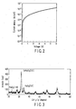
- FIG. 2 shows the leak current characteristic of the sample obtained in this manner. The leak current characteristic is remarkably deteriorated as compared with the sample of the present embodiment described later.
- FIG. 3 shows the results of in-plane diffraction of the sample obtained in this manner.
- the deterioration of the leak current characteristic of FIG. 2 is believed to be caused by the RuO 2 . That is, in the sample of FIG. 2, the amorphous PZT film is formed on the SRO film which contains RuO 2 and which is low in crystallinity, and is crystallized. Therefore, Pb reacts with RuO 2 at an interface between the PZT and SRO films and at grain boundary of PZT, and conductive compounds such as Pb 2 Ru 2 O 7-x are formed. This conductive compound forms a leak path, and thus the leak current increases.
- the SiO 2 film, titanium film (thickness of 10 nm), iridium film (120 nm), titanium film (2.5 nm), SRO film (10 nm), PZT film, and platinum film (50 nm) were successively formed on the silicon substrate.
- the SRO and PZT films after forming the amorphous film by sputtering, the film was annealed and crystallized in an oxygen atmosphere.
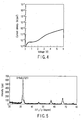
- FIG. 4 shows the leak current characteristic of the sample obtained in this manner. The leak current characteristic is remarkably improved as compared with the sample of the comparative example.
- a sample was prepared in which the SiO 2 film, titanium film (thickness of 10 nm), iridium film (120 nm), titanium film (2.5 nm), and SRO film (10 nm) were successively formed on the silicon substrate.
- the SRO film after forming the amorphous film by sputtering, the film was annealed and crystallized in an oxygen atmosphere.
- FIG. 5 shows the results of in-plane diffraction of the sample obtained in this manner. As seen from FIG. 5, the diffraction peak of RuO 2 as in FIG. 3 is not observed. Therefore, in the present embodiment, the SRO film extremely superior in crystallinity is obtained.
- FIG. 6 shows a hysteresis characteristic'in the sample of the present embodiment.
- FIG. 7 shows a fatigue characteristic in the sample of the present embodiment. As seen from FIGS. 6 and 7, both the hysteresis and fatigue characteristics were highly satisfactory.
- thermodynamic stability of the conductive perovskite metal oxide (represented by a general formula ABO 3 ) is proportional to that of the oxide of a B site element (BO x ).
- a site elements such as an alkaline-earth element and rare earth element, form extremely stable oxides. Therefore, it may be considered that the stability of the conductive perovskite metal oxide is determined by that of the oxide of the B site element.
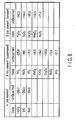
- FIG. 8 shows a generation enthalpy per oxygen molecule of a simple oxide at 25°C with respect to various metal elements.
- a larger absolute value of a numeric value shown in FIG. 8 indicates a higher stability of the oxide. That is, a high absolute numeric value shown in FIG. 8 indicates a large decrease amount of Gibbs free energy at a time when the metal element forms the oxide.
- Ru which is the B site element of SRO
- Ru indicates -72.8 (kcal/mol)
- Ti indicates -225.8 (kcal/mol). That is, a Ti oxide is higher in stability than an Ru oxide.
- thermodynamic stability of the conductive perovskite metal oxide is proportional to that of the oxide of the B site element. Therefore, when at least a part of Ru atoms contained in SRO is replaced with Ti atoms, the stability of SRO increases.
- the titanium film is provided between the SRO and iridium films. Therefore, it is considered that a part of Ru included in the SRO film is replaced with Ti by the heat treatment. When Ti is contained, the stability of the SRO film is enhanced. Therefore, the conductive compounds such as RuO 2 are inhibited from being generated. As a result, it is considered that the characteristics of the capacitor are enhanced.
- the titanium film is provided between the SRO and iridium films in the present embodiment, the stability of the SRO film and the characteristics of the capacitor can be enhanced. Moreover, when this structure is used for the bottom electrode, the oxidation of the tungsten plug can be inhibited by the barrier function of the iridium film. Therefore, even when the COP structure is used, it is possible to obtain a ferroelectric memory of superior characteristics and reliability.
- FIGS. 9A to 9C are sectional views showing the manufacturing steps of the semiconductor device according to a second embodiment of the present invention.
- FIGS. 9A and 9B are substantially similar to those of FIGS. 1A and 1B of the first embodiment, and the description thereof is omitted.
- the titanium film 116 having a thickness of 10 nm, and the iridium film 117 having a thickness of 100 nm, which is the noble metal film are successively deposited by a sputtering process.
- an SRO film (Sr(Ru,Ti)O 3 film) 119a doped with titanium which is the conductive perovskite metal oxide film, having a thickness of 10 nm, is deposited by a sputtering process.
- the SRO film 119a doped with titanium is crystallized by RTA in an oxygen atmosphere.
- the Pb(Zr x Ti 1-x )O 3 film (PZT film) 120 which is the dielectric film of the capacitor, is formed by a sputtering process. Furthermore, the PZT film 120 is crystallized by RTA in an oxygen atmosphere. Subsequently, an SRO film (Sr(Ru,Ti)O 3 film) 121a doped with titanium, which is the conductive perovskite metal oxide film, having a thickness of 10 nm, is deposited by a sputtering process. Furthermore, the SRO film 121a doped with titanium is crystallized by RTA in an oxygen atmosphere. Subsequently, the iridium film 123 having a thickness of 100 nm, which is a noble metal film, is deposited by a sputtering process.
- a silicon oxide film (not shown) is deposited on the whole surface by a CVD process. Furthermore, the silicon oxide film is patterned by photolithography and RIE processes. Subsequently, the patterned silicon oxide film is used as a mask to etch the iridium film 123, SRO film 121a, and PZT film 120 by an RIE process. Furthermore, the SRO film 119a, iridium film 117, and titanium film 116 are patterned by photolithography and RIE processes.
- the ferroelectric capacitor is formed comprising: the bottom electrode having the stacked structure of the titanium film 116, iridium film 117, and SRO film 119a; the ferroelectric film (PZT film 120); and the top electrode having the stacked structure of the SRO film 121a, and iridium film 123.
- the silicon oxide film 124 is deposited on the whole surface by a CVD process. Furthermore, a heat treatment is performed at about 650°C under an oxygen atmosphere, in order to remedy the damage generated in the PZT film 120 by the etching process. In this heat treatment, oxygen flows through the PZT film 120, but the oxygen barrier function of the iridium film 117 prevents the tungsten plug 115 from being oxidized.
- the subsequent steps comprise: forming a contact portion connected to the tungsten film 111; forming the drive and bit lines; and forming the metal wirings to complete the ferroelectric memory which includes the COP structure.
- the stacked structure of the SRO film doped with titanium and the iridium film is used in both the bottom and top electrodes, but could also be used in one of the bottom and top electrodes.
- the structure may be used for the bottom electrode, whereas the stacked structure of the SRO film not doped with titanium and the platinum film may also be used for the top electrode.
- the stacked structure of the SRO film doped with titanium and the iridium film is used. Therefore, as described in the first embodiment, the stability of the SRO film and the characteristics of the capacitor can be enhanced. Moreover, when this stacked structure is used for the bottom electrode, the oxidation of the tungsten plug can be inhibited by the barrier function of the iridium film. Therefore, even when the COP structure is used, it is possible to obtain the ferroelectric memory of superior characteristics and reliability.
- an SRO film (SrRuO 3 film) is used as the conductive perovskite metal oxide film.
- an (La,Sr)CoO 3 film, BaRuO 3 film, or LaNiO 3 film may also be used.
- the iridium film (Ir film) is used as a noble metal film (conductive film) in the first and second embodiments, but a ruthenium film (Ru film) or platinum film (Pt film) may also be used.
- ruthenium film Ru film
- platinum film Pt film
- noble metal oxide films such as an iridium oxide film (IrO 2 film) or ruthenium oxide film (RuO 2 film), may also be used.
- a titanium film (Ti film) is used as the metal film in the first embodiment, and an SRO film doped with titanium (Ti) is used in the second embodiment, but metal elements other than Ti may also be used as a second metal element.
- the B site element of the conductive perovskite metal oxide film such as an SrRuO 3 film
- the first and second metal elements may satisfy such a relation that the decrease of Gibbs free energy at a time when the second metal element forms an oxide is larger than that at a time when the first metal element forms an oxide.
- the second metal element in addition to Ti, the use of V, W, Zr, Cr, Mg, Hf, Mo, Mn, Ta, or Nb is also possible.
- a PZT film (Pb(Zr x Ti 1-x )O 3 film) is used as the dielectric film (ferroelectric film) in the first and second embodiments, but an SBT film (SrBi 2 Ta 2 O 9 film) may also be used.
- an SBT film Si 2 Ta 2 O 9 film
- a high dielectric constant film may also be used as the dielectric film.
- tungsten plug is used as the plug in the first and second embodiments, but a polysilicon plug may also be used.
- the noble metal film, metal oxide film, and metal film are formed by a sputtering process in the first embodiment, but these may also be formed by a CVD or sol-gel process.
- the noble metal film and metal oxide film are formed by a sputtering process in the second embodiment, but may also be formed by CVD or sol-gel process.
- the techniques described in the first and second embodiments can be applied not only to an FeRAM, but also to a DRAM.
Landscapes
- Semiconductor Memories (AREA)
Applications Claiming Priority (2)
| Application Number | Priority Date | Filing Date | Title |
|---|---|---|---|
| US427962 | 2003-05-02 | ||
| US10/427,962 US6924519B2 (en) | 2003-05-02 | 2003-05-02 | Semiconductor device with perovskite capacitor |
Publications (1)
| Publication Number | Publication Date |
|---|---|
| EP1473759A2 true EP1473759A2 (de) | 2004-11-03 |
Family
ID=32990462
Family Applications (1)
| Application Number | Title | Priority Date | Filing Date |
|---|---|---|---|
| EP04008796A Withdrawn EP1473759A2 (de) | 2003-05-02 | 2004-04-13 | Halbleiteranordnung |
Country Status (3)
| Country | Link |
|---|---|
| US (1) | US6924519B2 (de) |
| EP (1) | EP1473759A2 (de) |
| CN (1) | CN100424876C (de) |
Cited By (1)
| Publication number | Priority date | Publication date | Assignee | Title |
|---|---|---|---|---|
| EP4294159A1 (de) * | 2022-06-14 | 2023-12-20 | Samsung Electronics Co., Ltd. | Kondensatorstruktur, halbleiterspeicheranordnung mit dieser struktur und verfahren zur herstellung dieser struktur |
Families Citing this family (8)
| Publication number | Priority date | Publication date | Assignee | Title |
|---|---|---|---|---|
| JP3782401B2 (ja) * | 2003-05-07 | 2006-06-07 | 株式会社東芝 | 半導体装置 |
| JP2006060044A (ja) * | 2004-08-20 | 2006-03-02 | Canon Anelva Corp | 磁気抵抗効果素子の製造方法 |
| JP4220459B2 (ja) * | 2004-11-22 | 2009-02-04 | 株式会社東芝 | 半導体装置 |
| US7579623B2 (en) * | 2005-07-22 | 2009-08-25 | Translucent, Inc. | Stacked transistors and process |
| JP2008091693A (ja) * | 2006-10-03 | 2008-04-17 | Toshiba Corp | 半導体装置および半導体装置の製造方法 |
| JP2010118595A (ja) * | 2008-11-14 | 2010-05-27 | Toshiba Corp | 半導体装置 |
| US11302618B2 (en) | 2018-04-09 | 2022-04-12 | Intel Corporation | Microelectronic assemblies having substrate-integrated perovskite layers |
| EP4216245A3 (de) | 2022-01-19 | 2023-11-22 | Samsung Electronics Co., Ltd. | Kondensator, halbleiterbauelement mit dem kondensator und verfahren zur herstellung des kondensators |
Family Cites Families (4)
| Publication number | Priority date | Publication date | Assignee | Title |
|---|---|---|---|---|
| US6344271B1 (en) * | 1998-11-06 | 2002-02-05 | Nanoenergy Corporation | Materials and products using nanostructured non-stoichiometric substances |
| KR100319888B1 (ko) * | 1998-06-16 | 2002-01-10 | 윤종용 | 선택적 금속층 형성방법, 이를 이용한 커패시터 형성 및 콘택홀 매립방법 |
| JP3249496B2 (ja) | 1998-11-10 | 2002-01-21 | 株式会社東芝 | 半導体装置及び半導体装置の製造方法 |
| JP3745553B2 (ja) * | 1999-03-04 | 2006-02-15 | 富士通株式会社 | 強誘電体キャパシタ、半導体装置の製造方法 |
-
2003
- 2003-05-02 US US10/427,962 patent/US6924519B2/en not_active Expired - Fee Related
-
2004
- 2004-04-13 EP EP04008796A patent/EP1473759A2/de not_active Withdrawn
- 2004-04-29 CN CNB2004100366531A patent/CN100424876C/zh not_active Expired - Fee Related
Cited By (2)
| Publication number | Priority date | Publication date | Assignee | Title |
|---|---|---|---|---|
| EP4294159A1 (de) * | 2022-06-14 | 2023-12-20 | Samsung Electronics Co., Ltd. | Kondensatorstruktur, halbleiterspeicheranordnung mit dieser struktur und verfahren zur herstellung dieser struktur |
| US12471300B2 (en) | 2022-06-14 | 2025-11-11 | Samsung Electronics Co., Ltd. | Capacitor structure, semiconductor memory device including the structure, and method for manufacturing the structure |
Also Published As
| Publication number | Publication date |
|---|---|
| US6924519B2 (en) | 2005-08-02 |
| CN100424876C (zh) | 2008-10-08 |
| US20040217404A1 (en) | 2004-11-04 |
| CN1606163A (zh) | 2005-04-13 |
Similar Documents
| Publication | Publication Date | Title |
|---|---|---|
| US9679904B2 (en) | Method of manufacturing semiconductor device | |
| US6730951B2 (en) | Capacitor, semiconductor memory device, and method for manufacturing the same | |
| US8278181B2 (en) | Semiconductor device and method of manufacturing the same | |
| JP2007043166A (ja) | 多層下部電極及び多層上部電極を含む強誘電体構造物及びそれの製造方法 | |
| US7190015B2 (en) | Semiconductor device and method of manufacturing the same | |
| US7122851B2 (en) | Semiconductor device with perovskite capacitor | |
| JP2003282832A (ja) | 半導体装置及びその製造方法 | |
| US20150084160A1 (en) | Semiconductor device and method of manufacturing the same | |
| US6924519B2 (en) | Semiconductor device with perovskite capacitor | |
| US6872618B2 (en) | Methods of forming ferroelectric capacitors with metal oxide for inhibiting fatigue | |
| US7105400B2 (en) | Manufacturing method of semiconductor device | |
| US7049650B1 (en) | Semiconductor device | |
| JP3930453B2 (ja) | 半導体装置 | |
| US20050274999A1 (en) | Semiconductor device and method of manufacturing the same | |
| US7042037B1 (en) | Semiconductor device | |
| JP5277657B2 (ja) | 半導体装置及びその製造方法 | |
| JP2005129852A (ja) | 半導体装置 | |
| US7601585B2 (en) | Method of manufacturing a ferroelectric semiconductor device utilizing an oxide reduction film | |
| JP2008192914A (ja) | 半導体装置及びその製造方法 | |
| JP2006134961A (ja) | 半導体装置 | |
| WO2005038883A2 (en) | Manufacturing method of a ferroelectric capacitor |
Legal Events
| Date | Code | Title | Description |
|---|---|---|---|
| PUAI | Public reference made under article 153(3) epc to a published international application that has entered the european phase |
Free format text: ORIGINAL CODE: 0009012 |
|
| 17P | Request for examination filed |
Effective date: 20040413 |
|
| AK | Designated contracting states |
Kind code of ref document: A2 Designated state(s): AT BE BG CH CY CZ DE DK EE ES FI FR GB GR HU IE IT LI LU MC NL PL PT RO SE SI SK TR |
|
| AX | Request for extension of the european patent |
Extension state: AL HR LT LV MK |
|
| STAA | Information on the status of an ep patent application or granted ep patent |
Free format text: STATUS: THE APPLICATION HAS BEEN WITHDRAWN |
|
| 18W | Application withdrawn |
Effective date: 20090119 |