EP1452894A2 - Dispositif de traitement de signaux optiques et méthode de traitement de signaux optiques - Google Patents
Dispositif de traitement de signaux optiques et méthode de traitement de signaux optiques Download PDFInfo
- Publication number
- EP1452894A2 EP1452894A2 EP04012361A EP04012361A EP1452894A2 EP 1452894 A2 EP1452894 A2 EP 1452894A2 EP 04012361 A EP04012361 A EP 04012361A EP 04012361 A EP04012361 A EP 04012361A EP 1452894 A2 EP1452894 A2 EP 1452894A2
- Authority
- EP
- European Patent Office
- Prior art keywords
- optical
- light
- waveguide
- optical signal
- signal processing
- Prior art date
- Legal status (The legal status is an assumption and is not a legal conclusion. Google has not performed a legal analysis and makes no representation as to the accuracy of the status listed.)
- Withdrawn
Links
- 230000003287 optical effect Effects 0.000 title claims abstract description 710
- 238000012545 processing Methods 0.000 title claims abstract description 178
- 238000003672 processing method Methods 0.000 title claims abstract description 17
- 238000009826 distribution Methods 0.000 claims description 48
- 238000001228 spectrum Methods 0.000 claims description 34
- 230000009466 transformation Effects 0.000 claims description 29
- 238000006243 chemical reaction Methods 0.000 claims description 26
- 230000005684 electric field Effects 0.000 claims description 22
- 238000004364 calculation method Methods 0.000 claims description 8
- 238000001514 detection method Methods 0.000 claims description 3
- 238000010276 construction Methods 0.000 abstract description 46
- 238000007493 shaping process Methods 0.000 abstract description 10
- 238000005259 measurement Methods 0.000 abstract description 5
- 239000006185 dispersion Substances 0.000 description 105
- 230000005540 biological transmission Effects 0.000 description 70
- 239000000758 substrate Substances 0.000 description 53
- 239000002609 medium Substances 0.000 description 38
- 239000010453 quartz Substances 0.000 description 37
- VYPSYNLAJGMNEJ-UHFFFAOYSA-N silicon dioxide Inorganic materials O=[Si]=O VYPSYNLAJGMNEJ-UHFFFAOYSA-N 0.000 description 37
- 230000001965 increasing effect Effects 0.000 description 30
- 239000013307 optical fiber Substances 0.000 description 29
- 238000010586 diagram Methods 0.000 description 27
- 238000001208 nuclear magnetic resonance pulse sequence Methods 0.000 description 26
- 230000008878 coupling Effects 0.000 description 24
- 238000010168 coupling process Methods 0.000 description 24
- 238000005859 coupling reaction Methods 0.000 description 24
- 230000003595 spectral effect Effects 0.000 description 22
- 239000004973 liquid crystal related substance Substances 0.000 description 21
- 238000000034 method Methods 0.000 description 21
- 239000004065 semiconductor Substances 0.000 description 19
- 238000012986 modification Methods 0.000 description 18
- 230000004048 modification Effects 0.000 description 18
- 230000001427 coherent effect Effects 0.000 description 15
- 239000000463 material Substances 0.000 description 15
- 230000000694 effects Effects 0.000 description 14
- 230000010355 oscillation Effects 0.000 description 14
- 230000008859 change Effects 0.000 description 11
- 239000000835 fiber Substances 0.000 description 11
- 239000010410 layer Substances 0.000 description 11
- 230000010287 polarization Effects 0.000 description 11
- 230000002441 reversible effect Effects 0.000 description 11
- 239000011248 coating agent Substances 0.000 description 9
- 238000000576 coating method Methods 0.000 description 9
- 238000005530 etching Methods 0.000 description 9
- 238000004519 manufacturing process Methods 0.000 description 9
- 230000000875 corresponding effect Effects 0.000 description 8
- 230000015572 biosynthetic process Effects 0.000 description 7
- 239000011521 glass Substances 0.000 description 7
- 230000002829 reductive effect Effects 0.000 description 7
- 238000003786 synthesis reaction Methods 0.000 description 7
- 230000015556 catabolic process Effects 0.000 description 6
- 238000004891 communication Methods 0.000 description 6
- 238000006731 degradation reaction Methods 0.000 description 6
- 238000013461 design Methods 0.000 description 6
- 230000002194 synthesizing effect Effects 0.000 description 6
- 229920001721 polyimide Polymers 0.000 description 5
- 238000005086 pumping Methods 0.000 description 5
- 238000010438 heat treatment Methods 0.000 description 4
- 230000008569 process Effects 0.000 description 4
- 238000002310 reflectometry Methods 0.000 description 4
- 230000035945 sensitivity Effects 0.000 description 4
- 239000004988 Nematic liquid crystal Substances 0.000 description 3
- 238000005452 bending Methods 0.000 description 3
- 230000001276 controlling effect Effects 0.000 description 3
- 239000012792 core layer Substances 0.000 description 3
- 230000010354 integration Effects 0.000 description 3
- 230000009022 nonlinear effect Effects 0.000 description 3
- 238000003860 storage Methods 0.000 description 3
- 238000002834 transmittance Methods 0.000 description 3
- 229910001218 Gallium arsenide Inorganic materials 0.000 description 2
- 238000003491 array Methods 0.000 description 2
- 230000002596 correlated effect Effects 0.000 description 2
- 239000013078 crystal Substances 0.000 description 2
- 238000000354 decomposition reaction Methods 0.000 description 2
- 239000002612 dispersion medium Substances 0.000 description 2
- 238000010894 electron beam technology Methods 0.000 description 2
- 230000002708 enhancing effect Effects 0.000 description 2
- 230000007274 generation of a signal involved in cell-cell signaling Effects 0.000 description 2
- 238000001093 holography Methods 0.000 description 2
- 230000031700 light absorption Effects 0.000 description 2
- 238000000059 patterning Methods 0.000 description 2
- 230000010363 phase shift Effects 0.000 description 2
- 229910052761 rare earth metal Inorganic materials 0.000 description 2
- 150000002910 rare earth metals Chemical class 0.000 description 2
- 229910003327 LiNbO3 Inorganic materials 0.000 description 1
- 239000004642 Polyimide Substances 0.000 description 1
- XUIMIQQOPSSXEZ-UHFFFAOYSA-N Silicon Chemical compound [Si] XUIMIQQOPSSXEZ-UHFFFAOYSA-N 0.000 description 1
- 239000000853 adhesive Substances 0.000 description 1
- 230000001070 adhesive effect Effects 0.000 description 1
- 238000000137 annealing Methods 0.000 description 1
- JRPBQTZRNDNNOP-UHFFFAOYSA-N barium titanate Chemical compound [Ba+2].[Ba+2].[O-][Ti]([O-])([O-])[O-] JRPBQTZRNDNNOP-UHFFFAOYSA-N 0.000 description 1
- 229910002113 barium titanate Inorganic materials 0.000 description 1
- 238000012937 correction Methods 0.000 description 1
- 238000013016 damping Methods 0.000 description 1
- 230000001419 dependent effect Effects 0.000 description 1
- 230000008021 deposition Effects 0.000 description 1
- 238000011161 development Methods 0.000 description 1
- 239000003989 dielectric material Substances 0.000 description 1
- 238000001312 dry etching Methods 0.000 description 1
- 238000005516 engineering process Methods 0.000 description 1
- 238000011156 evaluation Methods 0.000 description 1
- 230000007062 hydrolysis Effects 0.000 description 1
- 238000006460 hydrolysis reaction Methods 0.000 description 1
- 230000000670 limiting effect Effects 0.000 description 1
- 239000007788 liquid Substances 0.000 description 1
- 230000007257 malfunction Effects 0.000 description 1
- 230000007246 mechanism Effects 0.000 description 1
- 229910021421 monocrystalline silicon Inorganic materials 0.000 description 1
- 239000011368 organic material Substances 0.000 description 1
- 230000036961 partial effect Effects 0.000 description 1
- 238000001020 plasma etching Methods 0.000 description 1
- 238000012827 research and development Methods 0.000 description 1
- 229910052710 silicon Inorganic materials 0.000 description 1
- 239000010703 silicon Substances 0.000 description 1
- 125000006850 spacer group Chemical group 0.000 description 1
- 238000010408 sweeping Methods 0.000 description 1
- 230000002123 temporal effect Effects 0.000 description 1
- 229920001169 thermoplastic Polymers 0.000 description 1
- 239000004416 thermosoftening plastic Substances 0.000 description 1
- 230000036962 time dependent Effects 0.000 description 1
- 230000001131 transforming effect Effects 0.000 description 1
Images


Classifications
-
- G—PHYSICS
- G02—OPTICS
- G02B—OPTICAL ELEMENTS, SYSTEMS OR APPARATUS
- G02B6/00—Light guides; Structural details of arrangements comprising light guides and other optical elements, e.g. couplings
- G02B6/10—Light guides; Structural details of arrangements comprising light guides and other optical elements, e.g. couplings of the optical waveguide type
- G02B6/12—Light guides; Structural details of arrangements comprising light guides and other optical elements, e.g. couplings of the optical waveguide type of the integrated circuit kind
- G02B6/12007—Light guides; Structural details of arrangements comprising light guides and other optical elements, e.g. couplings of the optical waveguide type of the integrated circuit kind forming wavelength selective elements, e.g. multiplexer, demultiplexer
- G02B6/12009—Light guides; Structural details of arrangements comprising light guides and other optical elements, e.g. couplings of the optical waveguide type of the integrated circuit kind forming wavelength selective elements, e.g. multiplexer, demultiplexer comprising arrayed waveguide grating [AWG] devices, i.e. with a phased array of waveguides
- G02B6/12011—Light guides; Structural details of arrangements comprising light guides and other optical elements, e.g. couplings of the optical waveguide type of the integrated circuit kind forming wavelength selective elements, e.g. multiplexer, demultiplexer comprising arrayed waveguide grating [AWG] devices, i.e. with a phased array of waveguides characterised by the arrayed waveguides, e.g. comprising a filled groove in the array section
-
- G—PHYSICS
- G02—OPTICS
- G02B—OPTICAL ELEMENTS, SYSTEMS OR APPARATUS
- G02B6/00—Light guides; Structural details of arrangements comprising light guides and other optical elements, e.g. couplings
- G02B6/10—Light guides; Structural details of arrangements comprising light guides and other optical elements, e.g. couplings of the optical waveguide type
- G02B6/12—Light guides; Structural details of arrangements comprising light guides and other optical elements, e.g. couplings of the optical waveguide type of the integrated circuit kind
- G02B6/12007—Light guides; Structural details of arrangements comprising light guides and other optical elements, e.g. couplings of the optical waveguide type of the integrated circuit kind forming wavelength selective elements, e.g. multiplexer, demultiplexer
- G02B6/12009—Light guides; Structural details of arrangements comprising light guides and other optical elements, e.g. couplings of the optical waveguide type of the integrated circuit kind forming wavelength selective elements, e.g. multiplexer, demultiplexer comprising arrayed waveguide grating [AWG] devices, i.e. with a phased array of waveguides
- G02B6/12014—Light guides; Structural details of arrangements comprising light guides and other optical elements, e.g. couplings of the optical waveguide type of the integrated circuit kind forming wavelength selective elements, e.g. multiplexer, demultiplexer comprising arrayed waveguide grating [AWG] devices, i.e. with a phased array of waveguides characterised by the wavefront splitting or combining section, e.g. grooves or optical elements in a slab waveguide
-
- G—PHYSICS
- G02—OPTICS
- G02B—OPTICAL ELEMENTS, SYSTEMS OR APPARATUS
- G02B6/00—Light guides; Structural details of arrangements comprising light guides and other optical elements, e.g. couplings
- G02B6/10—Light guides; Structural details of arrangements comprising light guides and other optical elements, e.g. couplings of the optical waveguide type
- G02B6/12—Light guides; Structural details of arrangements comprising light guides and other optical elements, e.g. couplings of the optical waveguide type of the integrated circuit kind
- G02B6/12007—Light guides; Structural details of arrangements comprising light guides and other optical elements, e.g. couplings of the optical waveguide type of the integrated circuit kind forming wavelength selective elements, e.g. multiplexer, demultiplexer
- G02B6/12009—Light guides; Structural details of arrangements comprising light guides and other optical elements, e.g. couplings of the optical waveguide type of the integrated circuit kind forming wavelength selective elements, e.g. multiplexer, demultiplexer comprising arrayed waveguide grating [AWG] devices, i.e. with a phased array of waveguides
- G02B6/12019—Light guides; Structural details of arrangements comprising light guides and other optical elements, e.g. couplings of the optical waveguide type of the integrated circuit kind forming wavelength selective elements, e.g. multiplexer, demultiplexer comprising arrayed waveguide grating [AWG] devices, i.e. with a phased array of waveguides characterised by the optical interconnection to or from the AWG devices, e.g. integration or coupling with lasers or photodiodes
- G02B6/12021—Comprising cascaded AWG devices; AWG multipass configuration; Plural AWG devices integrated on a single chip
-
- G—PHYSICS
- G02—OPTICS
- G02B—OPTICAL ELEMENTS, SYSTEMS OR APPARATUS
- G02B6/00—Light guides; Structural details of arrangements comprising light guides and other optical elements, e.g. couplings
- G02B6/10—Light guides; Structural details of arrangements comprising light guides and other optical elements, e.g. couplings of the optical waveguide type
- G02B6/12—Light guides; Structural details of arrangements comprising light guides and other optical elements, e.g. couplings of the optical waveguide type of the integrated circuit kind
- G02B6/12007—Light guides; Structural details of arrangements comprising light guides and other optical elements, e.g. couplings of the optical waveguide type of the integrated circuit kind forming wavelength selective elements, e.g. multiplexer, demultiplexer
- G02B6/12009—Light guides; Structural details of arrangements comprising light guides and other optical elements, e.g. couplings of the optical waveguide type of the integrated circuit kind forming wavelength selective elements, e.g. multiplexer, demultiplexer comprising arrayed waveguide grating [AWG] devices, i.e. with a phased array of waveguides
- G02B6/12023—Light guides; Structural details of arrangements comprising light guides and other optical elements, e.g. couplings of the optical waveguide type of the integrated circuit kind forming wavelength selective elements, e.g. multiplexer, demultiplexer comprising arrayed waveguide grating [AWG] devices, i.e. with a phased array of waveguides characterised by means for reducing the polarisation dependence, e.g. reduced birefringence
-
- G—PHYSICS
- G02—OPTICS
- G02B—OPTICAL ELEMENTS, SYSTEMS OR APPARATUS
- G02B6/00—Light guides; Structural details of arrangements comprising light guides and other optical elements, e.g. couplings
- G02B6/10—Light guides; Structural details of arrangements comprising light guides and other optical elements, e.g. couplings of the optical waveguide type
- G02B6/12—Light guides; Structural details of arrangements comprising light guides and other optical elements, e.g. couplings of the optical waveguide type of the integrated circuit kind
- G02B6/12007—Light guides; Structural details of arrangements comprising light guides and other optical elements, e.g. couplings of the optical waveguide type of the integrated circuit kind forming wavelength selective elements, e.g. multiplexer, demultiplexer
- G02B6/12009—Light guides; Structural details of arrangements comprising light guides and other optical elements, e.g. couplings of the optical waveguide type of the integrated circuit kind forming wavelength selective elements, e.g. multiplexer, demultiplexer comprising arrayed waveguide grating [AWG] devices, i.e. with a phased array of waveguides
- G02B6/12033—Light guides; Structural details of arrangements comprising light guides and other optical elements, e.g. couplings of the optical waveguide type of the integrated circuit kind forming wavelength selective elements, e.g. multiplexer, demultiplexer comprising arrayed waveguide grating [AWG] devices, i.e. with a phased array of waveguides characterised by means for configuring the device, e.g. moveable element for wavelength tuning
-
- G—PHYSICS
- G02—OPTICS
- G02B—OPTICAL ELEMENTS, SYSTEMS OR APPARATUS
- G02B6/00—Light guides; Structural details of arrangements comprising light guides and other optical elements, e.g. couplings
- G02B6/24—Coupling light guides
- G02B6/26—Optical coupling means
- G02B6/28—Optical coupling means having data bus means, i.e. plural waveguides interconnected and providing an inherently bidirectional system by mixing and splitting signals
- G02B6/293—Optical coupling means having data bus means, i.e. plural waveguides interconnected and providing an inherently bidirectional system by mixing and splitting signals with wavelength selective means
- G02B6/29304—Optical coupling means having data bus means, i.e. plural waveguides interconnected and providing an inherently bidirectional system by mixing and splitting signals with wavelength selective means operating by diffraction, e.g. grating
- G02B6/29305—Optical coupling means having data bus means, i.e. plural waveguides interconnected and providing an inherently bidirectional system by mixing and splitting signals with wavelength selective means operating by diffraction, e.g. grating as bulk element, i.e. free space arrangement external to a light guide
- G02B6/2931—Diffractive element operating in reflection
-
- G—PHYSICS
- G02—OPTICS
- G02B—OPTICAL ELEMENTS, SYSTEMS OR APPARATUS
- G02B6/00—Light guides; Structural details of arrangements comprising light guides and other optical elements, e.g. couplings
- G02B6/24—Coupling light guides
- G02B6/26—Optical coupling means
- G02B6/28—Optical coupling means having data bus means, i.e. plural waveguides interconnected and providing an inherently bidirectional system by mixing and splitting signals
- G02B6/293—Optical coupling means having data bus means, i.e. plural waveguides interconnected and providing an inherently bidirectional system by mixing and splitting signals with wavelength selective means
- G02B6/29379—Optical coupling means having data bus means, i.e. plural waveguides interconnected and providing an inherently bidirectional system by mixing and splitting signals with wavelength selective means characterised by the function or use of the complete device
- G02B6/29392—Controlling dispersion
- G02B6/29394—Compensating wavelength dispersion
-
- G—PHYSICS
- G02—OPTICS
- G02B—OPTICAL ELEMENTS, SYSTEMS OR APPARATUS
- G02B6/00—Light guides; Structural details of arrangements comprising light guides and other optical elements, e.g. couplings
- G02B6/24—Coupling light guides
- G02B6/42—Coupling light guides with opto-electronic elements
- G02B6/4201—Packages, e.g. shape, construction, internal or external details
- G02B6/4204—Packages, e.g. shape, construction, internal or external details the coupling comprising intermediate optical elements, e.g. lenses, holograms
- G02B6/4215—Packages, e.g. shape, construction, internal or external details the coupling comprising intermediate optical elements, e.g. lenses, holograms the intermediate optical elements being wavelength selective optical elements, e.g. variable wavelength optical modules or wavelength lockers
-
- G—PHYSICS
- G03—PHOTOGRAPHY; CINEMATOGRAPHY; ANALOGOUS TECHNIQUES USING WAVES OTHER THAN OPTICAL WAVES; ELECTROGRAPHY; HOLOGRAPHY
- G03H—HOLOGRAPHIC PROCESSES OR APPARATUS
- G03H1/00—Holographic processes or apparatus using light, infrared or ultraviolet waves for obtaining holograms or for obtaining an image from them; Details peculiar thereto
- G03H1/0005—Adaptation of holography to specific applications
-
- G—PHYSICS
- G03—PHOTOGRAPHY; CINEMATOGRAPHY; ANALOGOUS TECHNIQUES USING WAVES OTHER THAN OPTICAL WAVES; ELECTROGRAPHY; HOLOGRAPHY
- G03H—HOLOGRAPHIC PROCESSES OR APPARATUS
- G03H1/00—Holographic processes or apparatus using light, infrared or ultraviolet waves for obtaining holograms or for obtaining an image from them; Details peculiar thereto
- G03H1/04—Processes or apparatus for producing holograms
- G03H1/08—Synthesising holograms, i.e. holograms synthesized from objects or objects from holograms
- G03H1/0808—Methods of numerical synthesis, e.g. coherent ray tracing [CRT], diffraction specific
-
- G—PHYSICS
- G02—OPTICS
- G02B—OPTICAL ELEMENTS, SYSTEMS OR APPARATUS
- G02B6/00—Light guides; Structural details of arrangements comprising light guides and other optical elements, e.g. couplings
- G02B6/10—Light guides; Structural details of arrangements comprising light guides and other optical elements, e.g. couplings of the optical waveguide type
- G02B6/12—Light guides; Structural details of arrangements comprising light guides and other optical elements, e.g. couplings of the optical waveguide type of the integrated circuit kind
- G02B2006/12083—Constructional arrangements
- G02B2006/12104—Mirror; Reflectors or the like
-
- G—PHYSICS
- G02—OPTICS
- G02B—OPTICAL ELEMENTS, SYSTEMS OR APPARATUS
- G02B6/00—Light guides; Structural details of arrangements comprising light guides and other optical elements, e.g. couplings
- G02B6/10—Light guides; Structural details of arrangements comprising light guides and other optical elements, e.g. couplings of the optical waveguide type
- G02B6/12—Light guides; Structural details of arrangements comprising light guides and other optical elements, e.g. couplings of the optical waveguide type of the integrated circuit kind
- G02B2006/12083—Constructional arrangements
- G02B2006/12107—Grating
-
- G—PHYSICS
- G03—PHOTOGRAPHY; CINEMATOGRAPHY; ANALOGOUS TECHNIQUES USING WAVES OTHER THAN OPTICAL WAVES; ELECTROGRAPHY; HOLOGRAPHY
- G03H—HOLOGRAPHIC PROCESSES OR APPARATUS
- G03H2222/00—Light sources or light beam properties
- G03H2222/33—Pulsed light beam
Definitions
- This invention relates to a method and an apparatus for processing, measuring or storing high-speed optical signals.
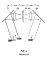
- FIG. 1 An example of prior art optical signal processing circuit is shown in Fig. 1.
- the reference numerals 201 and 205 indicate diffraction gratings
- 202 and 204 are lenses
- 203 is a spatial filter or an optical storage medium.
- a time series signal light is applied to this optical circuit
- a Fourier transformation of the time series signal light that is, a frequency spectrum distribution thereof is formed on the spatial filter 203 by the frequency decomposition function of the diffraction grating 201 and the Fourier transformation function of the lens 202.
- the frequency spectrum distribution is modulated by means of the spatial filter 203
- the waveform of the time series signal can be modulated.
- the waveform can be controlled by the spatial filter 203 even when the time series signal is very high in speed.
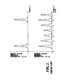
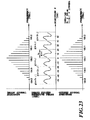
- the incident optical spectrum has a shape as shown in the upper part of Fig. 3, having an optical power distribution shown by the broken line in the middle part of Fig. 3 on the spatial filter 203 after passing through the diffraction grating 201 and the lens 202, and when this is modulated by the spatial filter 203, it has a shape as shown in the lower part of Fig. 3 in the spectrum after passing through the spatial filter 203.
- a time-dependent waveform corresponding to the spectrum is the pulse sequence shown in the lower part of Fig. 3.
- optical signal processing can be achieved by modulating the frequency spectrum of optical signal by the spatial filter 203. That is, various waveform shaping according to the filter is possible.
- pulse widths of optical signals utilized in optical transmission are 100 ps (ex; FA-10G system) in the practical application stage, and those of next-generation very large capacity transmission apparatus are considered to utilize picosecond pulses of 1-10 ps.
- Optical pulses of femtosecond region are application region of the time being in the research and development and material evaluation of stable light sources, and considered not to be applied in optical communications immediately. That is, basic apparatus and method enabling optical pulse generation, waveform shaping, waveform measurement, waveform recording, correlation processing, and the like are required for constructing next-generation very high capacity systems.
- the prior art structure using the diffraction grating pair and the lens effective for femtosecond pulses requires a very large sized apparatus for picosecond pulses, and is difficult to be packaged in a transmission apparatus of about 30 ⁇ 40 ⁇ 3cm. Further, it is required to use a connection optical system with the optical fiber, and flexible apparatus design according to the pulses is impossible.
- a semiconductor mode-locked laser is known as picosecond pulse generation means.
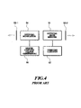
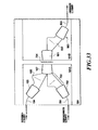
- Fig. 4 shows the structure of a prior art mode-locked laser for use as a short pulse light source.
- the mode-locked laser comprises an optical gain medium 51, an pumping circuit 52 for forming a population inversion to the optical gain medium 51, mirrors 53-1 and 53-2 constituting an optical resonator, an optical modulator 54 placed in the optical resonator, and a clock generator 55 for driving the optical modulator 54.
- the clock generator 55 drives the optical modulator 54 at a clock frequency equal to the resonance mode spacing of the optical resonator or an integer multiple thereof, an optical short pulse sequence of a repetition frequency equal to the clock frequency or an integer multiple thereof.
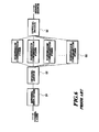
- Fig. 5 shows the structure of a multi-wavelength light source for simultaneously oscillating light of a plurality of wavelengths.
- the multi-wavelength light source comprises an optical gain medium 61, an arrayed-waveguide grating 62, a lens 63 for coupling the optical gain medium 61 with the arrayed-waveguide grating 62, a high reflection mirror 64 and a low reflection mirror 65 disposed at both end surfaces of the optical gain medium 61, and a high reflection mirror 66 disposed at the other end of the arrayed-waveguide grating 62.
- the arrayed-waveguide grating 62 comprises an input waveguide 71, an arrayed waveguide 73 including a plurality of waveguides gradually increasing in length by a waveguide length difference ⁇ L, a plurality of output waveguides 75, a slab waveguide 72 for connecting the input waveguide 71 and the arrayed waveguide 73, and a slab waveguide 74 for connecting the arrayed waveguide 73 and the output waveguide 75, which are formed on a substrate 70.
- an optical resonator is formed between the high refection mirror 64 and the high reflection mirror 66, and light of a plurality of wavelengths can be simultaneously oscillated by steadily exciting the optical gain medium 61.
- phase to each mode is not controlled in the multi-wavelength as shown in Fig. 5, it is impossible to generate an optical short pulse sequence of high repetition frequency by mode locking.
- Dispersion characteristics of a transmission line depend on ambient temperature, on material and cover with passage of time. Further, the dispersion characteristics are changed when the optical fiber is changed to another optical fiber in association with a malfunction or replacement of the transmission line. Or, even if the dispersion of the optical fiber is unchanged, the dispersion value applied to the optical signal is changed by changes in light source wavelength or filter characteristics.
- a transmission section of 80 km has a dispersion of ⁇ 80 ps/nm. Since an optical band width of optical signal of pulse width of 10 ps at 20 Gbit/s is about 1 nm, a pulse broadening of a maximum of 80 ps is generated. However, the time slot of 20 Gbit/s signal is 50 ps, a large inter-symbol interference is generated to produce large errors. Therefore, an apparatus for compensating (equalizing) the dispersion of transmission line is indispensable for a very high speed transmission apparatus.
- Fig. 6 An example of prior art is shown in Fig. 6.
- 01 is an optical amplifier
- 02 is an optical switch
- 03 is a dispersion compensation fiber.
- the optical signal is passed through another optical fiber having dispersion characteristics reverse to the dispersion of the transmission line to compensate the dispersion, thereby obtaining a good waveform.
- dispersion characteristics of the dispersion compensation fiber 03 are not variable, it is general to provide fibers of different dispersion characteristics for compensating the dispersion according to changes in dispersion characteristics of the transmission line.
- picosecond pulse waveform shaping e.g., dispersion compensation
- these means are difficult to achieve compensation for high order dispersion, variable dispersion compensation, and wide band compensation.
- the prior art shown in Fig. 1 is very small in compensatable dispersion amount. For example, for an optical pulse of 2 ps in pulse width, it can provide only a compensation of about 5 ps/nm.
- the optical signal processing apparatus as described above is required to measure waveform of optical signals of higher speed.
- the band width of the O/E converter is as much as 50 GHz and impossible to measure picosecond pulses of 1-10 ps.
- the streak camera is low in sensitivity in the optical communication wavelength region, a sufficient S/N is not obtained by a single sweeping, and a real-time waveform cannot be observed.
- Fig. 1 There is no report of study using the prior art shown in Fig. 1.
- the prior art is applied, as is, since light is distributed two-dimensionally on the Fourier transformation plane, measurement of high S/N is difficult unless a specific optical system is devised.
- An object of the present invention is to provide an optical signal processing apparatus and optical signal processing method which enables generation, waveform shaping, waveform measurement, waveform recording, correlation processing, and the like of optical pulses of 1-10 ps.
- the optical signal processing apparatus comprises an optical waveguide, first means for equally distributing an output of the optical waveguide, a arrayed waveguide for dividing the output light, second means for focusing the optical output of the arrayed waveguide, and a spatial filter for receiving incident light focused by the second means and spectrally dividing the incident light on a straight line and for modulating the incident light into a desired amplitude or phase according to the position on the straight line, thereby reflecting the incident light.
- another construction of the optical signal processing apparatus comprises a first optical waveguide, first means for equally distributing an output of the first optical waveguide, a first arrayed waveguide comprising an aggregate of optical waveguides changing in optical length by a constant interval for dividing the output light, second means for focusing the optical output of the first arrayed waveguide, a spatial filter for receiving incident light focused by the second means and distributing the incident light on a straight line and for modulating the light into a desired amplitude according to the position on the straight line, third means comprising an aggregate of optical waveguides changing in optical length by a constant interval for applying light to the second arrayed waveguide, fourth means for converging the output light of the second arrayed waveguide to a single point, and a second optical waveguide to which the output light of the fourth means is applied.
- a yet further construction of the optical signal processing apparatus comprises a reflective type spatial filter, a arrayed waveguide comprising an aggregate of optical waveguides changing in optical length by a constant interval, first means for applying coherent light to the reflective type spatial filter and inputting the coherent light modulated by the reflective type spatial filter into the arrayed waveguide, and second means for converging output light of the arrayed waveguide to a single point.
- a yet further construction of the optical signal processing apparatus comprises a transmission type spatial filter, a arrayed waveguide comprising an aggregate of optical waveguides changing in optical length by a constant interval, first means for applying coherent light to the transmission type spatial filter, second means for applying the coherent light modulated by the transmission type spatial filter into the arrayed waveguide, and third means for converging output light of the arrayed waveguide to a single point.
- the optical signal processing method is characterized in that an optical signal is input to an optical signal processing apparatus having a arrayed waveguide and a spatial filter, to convert the optical signal into a frequency spectral image, the frequency spectral image is subjected to a desired modulation by the spatial filter, and the modulated frequency spectral image is converged to a single point to obtain a new optical signal.
- the optical signal processing apparatus used is preferably the above-described optical signal processing apparatus.
- Another arrangement of the optical signal processing method according to the present invention is characterized in that coherent light is input in an optical signal processing apparatus having a arrayed waveguide and a spatial filter written with a hologram image corresponding to the frequency spectrum of a desired optical signal to generate an optical signal.
- optical signal processing apparatus is characterized by comprising in the optical signal processing apparatus of the basic structure having the above-described mirror, at the input side of the optical waveguide, optical modulation means for modulating an oscillation light in an optical resonator with a frequency nearly equal to the resonance mode spacing or an integer multiple thereof, and optical gain means, wherein the modulation means, the gain means, and the optical waveguide are sequentially coupled by optical coupling means, an optical reflection mirror is disposed on the end surface not facing the coupling means of the optical modulator, the mirror formed on the end surface of the second means is a high reflection type, a resonator is formed between these high reflection type mirrors, thereby enabling generation of a short pulse light.
- a plurality of output waveguides may be disposed at predetermined spacings between the focal plane of one slab waveguide of the arrayed waveguide grating and the high reflection mirror.
- the plurality of output waveguides may be disposed at equal spacings.
- the high reflection mirrors corresponding to the individual output waveguides may be different in reflectivity from each other.
- the plurality of output waveguides may be set with predetermined waveguide length differences for compensating dispersion in the optical resonator.
- a plurality of lens arrays disposed at a predetermined spacing, and a liquid crystal light modulator having a high reflection mirror on one side may be provided.
- an optical synthesizer for synthesizing part or all of a plurality of output waveguides.
- gratings formed in the individual output waveguides may be different in diffractive efficiency from each other.
- a plurality of high reflection mirrors may be disposed at predetermined spacings on the focal plane of one slab waveguide of the arrayed waveguide grating.
- a plurality of high reflection mirrors may be disposed at equal spacings.
- the plurality of high reflection mirrors may be different in reflectivity from each other.
- a plurality of diffraction gratings may be formed at a predetermined spacing in the focal plane of the slab waveguide.
- the plurality of diffraction gratings may be disposed at equal spacings.
- the plurality of diffraction gratings may be different in diffractive efficiency from each other.
- the individual positions of the plurality of diffraction gratings may be dislocated in the normal direction of the focal plane of the slab waveguide.
- a groove may be formed on the focal plane of the slab waveguide, and films formed by stacking a plurality of mirrors may be disposed at a predetermined spacing in the groove.
- optical modulation means and the optical gain means may be integrated.
- part of the individual components may be connected with an optical fiber.
- the position of the high reflection mirror may be controlled by a fine control mechanism.
- the spacing of the high reflection mirrors may be varied in the normal direction of the slab waveguide.
- an apparatus for observing the waveform of the optical signal to be processed can be constructed.
- Such a waveform observable optical signal processing apparatus comprises an optical waveguide, an arrayed waveguide comprising a plurality of optical waveguides gradually increasing in waveguide length, distribution means for distributing output light of the optical waveguide to the arrayed waveguide, focusing means for focusing the output light of the arrayed waveguide, a spatial filter disposed in the vicinity of the focal plane of the focusing means for modulating the light image, reflection means for reflecting light modulated by the spatial filter, and optical division means for taking out the reflected light from the reflection means in the optical waveguide.
- the apparatus comprises a first optical waveguide, a first arrayed waveguide comprising a plurality of optical waveguides gradually increasing in waveguide length, distribution means for distributing the output light of the first optical waveguide to the first arrayed waveguide, first focusing means for focusing the output light of the first arrayed waveguide, a spatial filter disposed in the vicinity of the focal plane of the first focusing means for modulating the light image, and further comprising a second arrayed waveguide comprising a plurality of optical waveguides gradually increasing in waveguide length, second focusing means for focusing the light modulated by the spatial filter to the second arrayed waveguide, a second optical waveguide, and wave synthesis means for synthesizing the output light of the second arrayed waveguide and coupling to the second optical waveguide.
- the apparatus comprises a first optical waveguide, a first arrayed waveguide comprising a plurality of optical waveguides gradually increasing in waveguide length, distribution means for distributing output light of the first optical waveguide to the first arrayed waveguide, a reference light input optical waveguide, a second arrayed waveguide comprising a plurality of optical waveguides gradually increasing in waveguide length, second distribution means for distributing the output light of the reference light input optical waveguide to the second arrayed waveguide, focusing means for focusing the output light of the first arrayed waveguide and the output light of the second arrayed waveguide, an optical recording medium disposed in the vicinity of the focal plane of the focusing means, and optical division means for taking out the reflected light from the first optical waveguide.
- a yet further construction of the waveform observable apparatus comprises a first optical waveguide, a first arrayed waveguide comprising a plurality of optical waveguides gradually increasing in waveguide length, first distribution means for distributing the output light of the first optical waveguide to the first arrayed waveguide, a third arrayed waveguide comprising a plurality of optical waveguides gradually increasing in waveguide length, second distribution means for distributing the output light of the reference light input optical waveguide to the third arrayed waveguide, first focusing means for focusing the output light of the first arrayed waveguide and the output light of the third arrayed waveguide, an optical recording medium disposed in the vicinity of the focal plane of the first focusing means, a second arrayed waveguide comprising a plurality of optical waveguides gradually increasing in waveguide length, second focusing means for focusing the light modulated by the optical recording means to the second arrayed waveguide, a second optical waveguide, and wave synthesis mans for synthesizing the output light of the second arrayed waveguide and
- another construction of the waveform observable apparatus comprises a first optical waveguide, a first arrayed waveguide comprising a plurality of optical waveguides gradually increasing in waveguide length, first distribution means for distributing the output light of the first optical waveguide to the first arrayed waveguide, a first reference light input optical waveguide, a second arrayed waveguide comprising a plurality of optical waveguides gradually increasing in waveguide length, second distribution means for distributing the output light of the first reference light input optical waveguide to the second arrayed waveguide, a second reference light input optical waveguide, first focusing means for focusing the output light of the first arrayed waveguide and the output light of the second arrayed waveguide and the output light of the second reference light input optical waveguide, an optical recording medium disposed in the vicinity of the focal plane of the first focusing means, second focusing means for focusing the light modulated by the optical recording medium, and a light receiver array disposed in the vicinity of the focal plane of the second focusing means.
- the focusing means may be a slab waveguide having a circular end surface.
- the focusing means may comprise a slab waveguide and a phase spatial modulation device.
- the spatial filter may be a phase filter, or an amplitude filter, or a spatial filter formed of amplitude filters and phase filters connected in multiple stages.
- the focal length of the phase spatial modulation device may be equal to the focal length of the slab waveguide of the coupling means.
- the spatial filter and the reflection means may be combined to form a pattern mirror comprising a number of partial mirrors.
- the spatial filter may be a spatial filter combining with a function of a phase spatial modulation device.
- the focusing means may be a lens.
- the focusing means may be a slab waveguide of the focal plane, having a phase adjusting arrayed waveguide at the end of the slab waveguide, and the phase adjusting arrayed waveguide end may be connected to the spatial filter.
- the focusing means may be a slab waveguide of the focal plane, having a phase adjusting arrayed waveguide at the slab waveguide end, and the phase adjusting arrayed waveguide may have an optical modulator array.
- phase difference between waveguides of the phase adjusting arrayed waveguide may be an integer multiple of 2 ⁇ .
- the optical division means may be an optical circulator.
- the focusing means is a slab waveguide, having optical bend means at the slab waveguide end for bending light in direction perpendicular to the waveguide.
- the spatial filter may be a liquid crystal spatial modulator comprising a glass substrate, a transparent electrode, a liquid crystal, and a liquid crystal alignment film.
- a quarter-wave plate may be provided in the liquid crystal spatial modulator.
- liquid crystal of the liquid spatial modulator may be a twist nematic type.
- the optical signal processing method by the waveform observable optical signal processing apparatus is characterized in that a time series optical signal is input in the optical waveguide to convert the time series optical signal into a frequency spectrum image, the frequency spectrum image is subjected to desired phase or amplitude or both modulations, and the modulated light is synthesized to obtain a new time series optical signal.
- filter characteristics of the spatial filter may be a hologram image of a pattern corresponding to the frequency spectrum of a desired time series optical signal, and coherent pulse light is applied to the optical waveguide to generate the desired optical signal.
- an optical signal may be input in the optical waveguide, a reference light of coherent pulse light is applied to the reference light input waveguide, hologram recording is made on the recording medium, a reference light of another coherent pulse light is applied to the reference light input waveguide, to output a phase conjugate light of the signal light.
- signal light is input in the optical waveguide, a reference light of coherent pulse light is applied to the reference light input waveguide, hologram recording is made on the recording medium, a reference light of another coherent pulse light is applied to the reference light input waveguide, to output a signal light or a correlated light of the signal light and the reference light.
- a signal light is input in the optical waveguide, a reference light of coherent pulse light is applied to the first reference light input waveguide, a reference light of single color is applied to the second reference light input waveguide to form reference light of coherent pulse light in the first reference light input waveguide to observe the pulse waveform.
- the present invention based on the optical signal processing apparatus of the above-described basic structure, can provide an optical signal processing apparatus which enables dispersion compensation of the processed optical signal.
- the optical signal processing apparatus that enables such dispersion compensation comprises a first optical amplifier, an optical wavelength filter, a first optical waveguide, a first arrayed waveguide comprising a plurality of optical waveguides gradually increasing in waveguide length, distribution means for distributing the output light of the first optical waveguide to the arrayed waveguide, first focusing means for focusing the output light of the first arrayed waveguide, a spatial filter disposed in the vicinity of the focal plane of the first focusing means for modulating optical image, reflection means for reflecting light modulated by the spatial filter, optical division means for taking out the reflected light from the first optical waveguide, and a second optical amplifier.
- Another construction of the dispersion compensatable optical signal processing apparatus comprises a first optical amplifier, an optical wavelength filter, a first arrayed waveguide comprising a plurality of optical waveguides gradually increasing in waveguide length, distribution means for distributing the output light of the first optical waveguide, first focusing means for focusing the output light of the first arrayed waveguide, a spatial filter disposed in the vicinity of the focal plane of the first focusing means for modulating the optical image, a second arrayed waveguide comprising a plurality of optical waveguides gradually increasing in waveguide length, second focusing means for focusing light modulated by the spatial filter to the second arrayed waveguide, a second optical waveguide, optical synthesis means for synthesizing the output light of the second arrayed waveguide and coupling to the second optical waveguide, and a second optical amplifier.
- an optical signal processing apparatus can be constituted of the dispersion compensatable optical signal processing apparatus, a light source, and an optical modulation signal generation circuit.
- an optical signal processing apparatus can be composed of the dispersion compensatable optical signal processing apparatus and an optical receiver.
- an optical signal processing apparatus can comprise the dispersion compensatable optical signal processing apparatus, an optical signal transmitter circuit comprising a light source, an optical modulator, an optical signal receiver circuit comprising the dispersion compensatable optical signal processing apparatus and an optical receiver, and an optical transmission line.
- the spatial filter may comprise a phase filter and an amplitude filter.
- the spatial filter may be a liquid crystal spatial modulator comprising a glass substrate, a transparent electrode, a liquid crystal, and a liquid crystal alignment film.
- an optical signal processing method by the above dispersion compensatable optical signal processing apparatus is characterized in that frequency spectral phase of optical signal generated by the optical signal transmitter circuit is modulated, and dispersion in the optical fiber and frequency spectral phase modulation by the optical signal transmitter circuit are compensated by the optical receiver circuit.
- Another arrangement of the optical signal processing method is characterized in that the frequency spectral amplitude of the optical signal generated by the optical signal transmitter circuit is modulated, dispersion in the optical fiber and frequency spectral amplitude modulation by the optical signal transmitter circuit are compensated by the optical signal receiver circuit.
- a further arrangement is characterized in that frequency spectral phase and frequency spectral amplitude of the optical signal generated by the optical signal transmitter circuit are modulated, and dispersion in the optical fiber and frequency spectral phase modulation and frequency spectral amplitude modulation are compensated by the optical receiver circuit.
- a yet further construction of the dispersion compensatable optical signal processing apparatus comprises a first optical signal processing apparatus comprising:
- a yet further construction of the dispersion compensatable optical signal processing apparatus comprises a first optical signal processing apparatus comprising:
- the present invention based on the optical signal processing apparatus of the above-described basic structure, can provide an optical signal processing apparatus which enables real-time observation of waveform of the processed optical signal.
- Such a waveform observable optical signal processing apparatus comprises first time - space conversion means for converting time series optical signal of the signal light into spatial signal light, second time - space conversion means for converting time series optical signal of reference light into spatial signal light, focusing means for focusing the spatial signal light individually output from the first time - space conversion means and the second time - space conversion means to make interference with each other, light receiving means disposed in the vicinity of the focal plane of the focusing means for receiving an interference light image of a plurality of optical signals incident into the focusing means, and an optical signal restoration circuit for restoring a time series signal of the signal light from the detection signals of the light receiving means.
- the first and second time - space conversion means may comprise arrayed waveguide gratings, and the focusing means may comprise a slab waveguide having a function for making Fourier transformation of the spatial signal light.
- the first and second time - space conversion means may comprise diffraction gratings
- the focusing means may comprise a lens for making Fourier transformation of the spatial signal light.
- the light receiving means may comprise a photodiode array.
- the optical signal restoration circuit may restore electric field distribution of optical pulse of the signal light by calculation from electric field distribution of the Fourier transform hologram detected by the light receiving means.
- a signal processing method by the waveform observable optical signal processing apparatus is characterized by comprising a step of converting a time series optical signal of unknown signal light into spatial signal light, a step of converting time series optical signal of known reference light into spatial signal light, a step of focusing individually the spatial signal of the signal light and the spatial signal of the reference light to make interference with each other, thereby forming a hologram image of a pattern corresponding to the frequency spectrum of time series signal, a step of receiving the hologram image to be converted into an electrical signal, and a step of restoring the unknown signal light from the hologram image converted to electrical signal using a predetermined calculation formula.
- the step of restoring the unknown signal light from the hologram image may have a mathematical calculation operation for multiplying the hologram image formed on the focal plane with electric field distribution of reconstructing light mathematically derived from the electric field distribution of known reference light, followed by Fourier transformation operation and space - time conversion operation.
- the electric field distribution of reconstructing light on the focal plane to be multiplied with the hologram image may include a factor of dividing by the square of absolute value of amplitude distribution of electric field distribution at the focal plane of the known reference light.
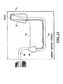
- an input optical signal u(t) after being incident to a quartz waveguide 1, is divided to an arrayed grating 3 of N waveguides by a star coupler 2.
- the arrayed waveguide 3 is set so that individual waveguides have an optical length difference of ⁇ L between an incident surface S1 and an output surface S2.
- the structure is known to have the same wave division function as a diffraction grating (for example, H. Takahashi et al., IEEE J. Lightwave Tech. Vol. 12 (No. 6), pp. 989-995 (1994); M.K. SMIT Electron. Lett. vol.24, pp.385-386(1988); C. Dragone et al., IEEE Photon. Technol. Lett., vol. 3, pp.896-899(1991)).
- a diffraction grating for example, H. Takahashi et al., IEEE J. Lightwave Tech. Vol. 12 (No. 6), pp. 989-995 (1994); M.K. SMIT Electron. Lett. vol.24, pp.385-386(1988); C. Dragone et al., IEEE Photon. Technol. Lett., vol. 3, pp.896-899(1991)).
- the inventors have found that when a time series optical signal is applied to the arrayed waveguide 3, time-frequency spectrum of the optical signal can be formed as a spatial image even without using a lens. Further, the inventors have found a high-resolution arrayed waveguide designing method and devised applications thereof in optical signal processing based on this principle.
- the frequency resolution is proportional to Nm.
- N is the number of waveguides of the arrayed waveguide 3. Therefore, when m is increased, an increased resolution can be obtained as compared with an ordinary diffraction grating in which the frequency resolution is proportional to N.
- a waveguide array with a very high optical resolution can be obtained, thereby enabling spectral division of a high-speed long optical pulse sequence.
- the output optical signal is u(t)*h(t), wherein * indicates a convolution of two signals.
- processing can be made in the frequency region of the incident signal light.
- Input/output between the external and the quartz waveguide 1 is made, for example, by using an optical fiber with a coupler.
- the focal plane S3 is on the circumference about the center of S2
- the spatial filter 5 when the spatial filter 5 is flat, generally a distortion occurs in the output waveform.
- this configuration is approximately has a quadratic dispersion characteristics.
- the input light or output light may be passed through a dispersion medium having the same magnitude and reverse sign.
- the spatial filter 5 may be designed to include the dispersion compensation.
- an optical signal processing apparatus as shown in Fig. 9 can be used.
- a reflective type structure is shown in Fig. 8 showing the principle of optical signal processing, whereas the apparatus shown in Fig. 9 is a transmission type.
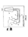
- the optical signal f(t) having a certain distortion is applied to a quartz optical circuit 8 from an optical fiber 7 through an optical connector 6.
- the quartz optical circuit 8 as shown in Fig. 10, comprises waveguides 9 and 13, star couplers 10 and 14, arrayed waveguides 11 and 15 and slab waveguides 12 and 16, which are symmetrically disposed to a spatial filter 17.
- the arrayed waveguides 11 and 15 are as necessary provided halfway with half wave plates 18 and 18 to eliminate polarization dependence.
- the signal When it is passed through the slab waveguide 16, the arrayed waveguide 15, and the star coupler 14, the signal is inverse Fourier transformed, and the restored optical signal u(t) can be taken out from the waveguide 13. When amplitude damping is large, the signal is output to the outside by the optical connector 6 through an optical amplifier 19.
- the spatial filter 17 may be a fixed or rewritable pattern.
- a fixed pattern one which is formed with a pattern of a predetermined phase or transmittance formed by deposition or the like on a substrate such as a glass substrate may be disposed.
- an optical modulator comprising a liquid crystal or semiconductor is used as a spatial filter, phase or transmittance of each pixel on the optical modulator is controlled by a voltage output from a spatial filter controller 20.
- a reflective type computer generated hologram (CGH) 21 is disposed on the focal plane S3.
- CGH computer generated hologram 21
- Fourier transformation U(t) of an optical pulse sequence u(t) is written as a spatial frequency pattern.
- the optical pattern U(v) reflected from the hologram is transmitted in the order of the slab waveguide 23, a arrayed waveguide 24, and a star coupler 25, Fourier transformed by the principle described in Embodiment 1, and the optical pulse sequence u(t) is output from a waveguide 26.
- read light may be applied to a arrayed waveguide 43 through a waveguide 41 and a star coupler 42, and applied to the computer generated hologram 21 as a Fourier transformed image.
- the read light may be a short optical pulse.
- a transmission type computer generated hologram 31 can be used. That is, when read light is applied to a slab waveguide 34 from a arrayed waveguide 32 and a waveguide 33 at the opposite side, the optical pattern u(v) passed through the hologram is transmitted in the order of a slab waveguide 35, a arrayed waveguide 32, and a star coupler 36, inverse Fourier transformed as described above, and the optical pulse sequence u(v) is output from an optical waveguide 37.
- an optical pulse sequence which comprises 100 pulses of a single pulse width of 0.2 ps and a period of 0.5 ps.
- a photosensitive optical recording medium 51 is disposed on the focal plane S3.
- the input optical signal u(t) is introduced into the apparatus from the external by an optical connector 52, and amplified by an optical amplifier 53. Then, the signal is divided by an optical coupler 54 into signal light and reference light, and the signal light is applied, as is, to a quartz optical circuit 55.
- the signal light after being applied to a waveguide 56, is divided into a arrayed waveguide 58 by a star coupler 57.
- each arrayed waveguide 58 is transmitted in a slab waveguide 59, spatially focuses Fourier transformation U(v) of the input optical signal on the focal plane S3.
- the reference light divided from the signal light is divided by the optical coupler 54, after passing through an optical modulator 60, is applied to the quartz optical circuit 55, as shown in Fig. 15, passing through a reference waveguide 61, and then applied to the slab waveguide 59.
- Fig. 15B shows an enlarged view of the star coupler 57 in Fig. 15A.
- the input waveguide end of the arrayed waveguide is disposed on a circumference, on one of a circumference about the input end from the reference waveguide 61 to the star coupler 57, and a circumference about the input end from the waveguide 56 to the star coupler 57.
- the number of waveguides disposed on each circumference is set nearly equal to each other.
- the optical modulator 60 serves to cut an optical pulse for reference light or read light from part of the signal light.
- optical pulse sequence is stored by the above described principle.
- the present embodiment shows a reflective type arrangement
- an arrangement is also possible in which the reference light and the read light are applied through a arrayed waveguide.
- the optical recording medium 51 can be, for example, a photo refractive device of a semiconductor multiple quantum well structure or a photosensitive film.
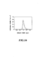
- Input light is the output of a Cr/YAG laser which is band limited by a wavelength filter to produce a pulse with a central wavelength of 1549 nm, a spectral width of 2.3 nm, and a pulse width of 1.1 ps.
- FIG. 16 A pulse waveform of the input light when optical signal generation is made with the above arrangement is shown in Fig. 16.
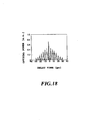
- An output waveform when processed by providing reflective type amplitude filters for pulse generation on the focal plane is shown in Figs. 17 and 18. It has been confirmed from Figs. 17 and 18 that the optical signal processing apparatus and the optical signal processing method according to the present invention function as designed.
- a first effect of the present invention is that the signal processing capacity (processable pulse sequence length) is high.
- the arrangement according to the present invention is long in processable pulse sequence length as compared with the prior art arrangement, and design according to the pulse width of optical pulse to be processed by changing the diffraction order (m).
- maximum processable pulse sequence length (T 0 ) and minimum pulse width ( ⁇ ) are as follows.
- processing capacity is proportional to the processable pulse sequence length. That is, the circuit of the present invention has about 10 times the capacity of the prior art.
- a second effect of the present invention is that the apparatus can be made compact in structure.
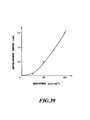
- the total length is 4f.
- the optical circuit can be bent and disposed, and since the waveguide material is higher in refractive index than the air, the apparatus can be constructed smaller in size, an apparatus having the performance of Fig. 19 can be fabricated with a quartz substrate of about 10 cm square. With a semiconductor waveguide, the size is about 5 cm square.
- a third effect is that integration with other optical circuits is possible.
- an optical amplifier is incorporated, thereby achieving optical signal processing with reduced loss.
- An effect when the present invention is applied to picosecond pulse generation means is that a pulse sequence close to the transform limit can be easily generated by dispersion compensation in the resonator, and that the pulse shape can be designed by control over individual modes.
- An effect when the present invention is applied to a dispersion compensation circuit is that high-order dispersion compensation, variable dispersion compensation, and wide band compensation are possible.
- To an optical pulse of 2 ps in pulse width compensation of up to about 100 ps/nm is possible. Further, it is possible to dispose a kinoform (Fresnel lens) between the slab waveguide and filter/mirror to achieve waveform shaping without distortion.
- a kinoform Fresnel lens
- An effect when the present invention is applied to a transmission apparatus is that dispersion compensation following a change in the dispersion of the transmission line is possible, system construction is possible with reduced transmission waveform degradation due to self-phase modulation, and that an amplitude modulation - angular modulation conversion circuit can be easily constructed.
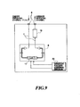
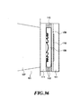
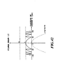
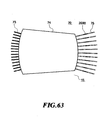
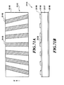
- Fig. 20 shows an embodiment 5 according to the present invention.
- a first slab waveguide 105 for distributing output of an optical waveguide 104 an arrayed waveguide 106 formed of a plurality of optical waveguides gradually increasing in waveguide length for generating phase difference by differing the optical length of distributed light of the slab waveguide 105, and a second slab waveguide 107 having a circular end surface and a lens function are integrated on a quartz substrate 101.
- 200 is an arrayed waveguide grating.
- an optical circulator 102 for taking out return reflected light is disposed in the course of the optical fiber 103.
- an optical fiber coupler has the same function and can be used, however, it has an extra loss of at least 6 dB.
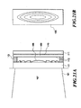
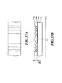
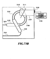
- a phase spatial modulation device represented by a Fresnel lens 108 or kinoform, a spatial filter 109, and a mirror 110 as reflection means are present.
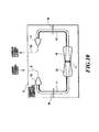
- Fig. 21 is a schematic enlarged view showing the Fresnel lens 108 as a phase spatial modulation device, the spatial filter 109, and the like disposed on the quartz substrate 101, as shown in Fig. 21A, the Fresnel lens (kinoform) 108, a holding substrate 113, the spatial filter 109, and the mirror 110 are provided to be disposed between quartz substrates 111, a low reflection filer 112 is stuck on the surface of the Fresnel lens (kinoform) 108 and the surface of the spatial filter 109.
- the side surface shape of the Fresnel lens (kinoform) 108 is, as shown in Fig.
- the contour part is elliptical, and curvature in the minor diameter direction is equal to the focal length of the slab waveguide 107, which can be fabricated by etching a material which is transparent in the operation wavelength region.
- the structure and production method of the Fresnel lens will be described in detail in a later embodiment.
- Fresnel lens Although greater in film thickness than a Fresnel lens, it may be fabricated by etching a spheric or an aspheric lens or the like, and used in place of the Fresnel lens 108. The fabrication method is similar to the Fresnel lens.
- the function of the structure shown in Figs. 20 and 21 is substantially equivalent to the function of the prior art structure shown in Fig. 1, as to the large size which is a problem in the prior art, for example, in an example of repetition signal (Fig. 22 upper part) of a pulse interval 50 ps and a pulse with 2 ps, an optical system of a beam diameter of, for example, at least 15 mm is required, an apparatus of about 50 ⁇ 100 cm in size is required considering the effective diameter of the lens.
- an optical length difference of a maximum of about 10 mm may be provided in the quartz waveguide, which can be integrated on a substrate of about 5 ⁇ 5 cm, thus there is a big difference in size.
- the first slab waveguide 105, the arrayed waveguide 106, and the second slab waveguide 107 are integrated on the quartz substrate, of which the arrayed waveguide 106 differs in waveguide length by ⁇ L between adjacent individual waveguides to have a optical path difference of n ⁇ L, wherein n is a refractive index of the waveguide. That is, the arrayed waveguide 106 has a wave division function same as a diffraction grating.
- Output end of the arrayed waveguide is formed in a circumferential form of a radius f and connected to the second slab waveguide 107, the second slab waveguide 107 functions as a lens of a focal length f. That is, in the case of a lens, whereas it has a Fourier transformation function of image between focal planes of both ends of the lens in the vicinity of the optical axis, the second slab waveguide 107 also has a single dimensional Fourier transformation function of output image of the arrayed waveguide 106. Since the focus of the second slab waveguide is positioned on the circumferential surface on the optical axis of the second slab waveguide 107, the Fresnel lens (kinoform) 108 is provided at the output side to make the focal plane flat.
- the focal length in the waveguide surface of the Fresnel lens (kinoform) 108 is set equal to the above described f.
- the arrangement of the spatial filter 109 for modulating through the low reflection coating 112 and the mirror for reflection is as shown in Fig. 21A, however, the Fresnel lens (kinoform) 108 and the spatial filter (in the case of a phase filter) can be fabricated by etching a material which is transparent to the operating wavelength, or can be fabricated in a desired shape by adjusting exposure to the photosensitive material by direct depicting of electron beam, since the developed thickness is determined in inverse proportion to the exposure.
- the Fresnel lens 108 and the spatial filter 109 by etching the substrate using the photosensitive material as a mask to process the substrate form.
- the light absorption film can be etched into strips with controlled line - space ratio. As to whether a phase filter or an amplitude filter is selected, the former has a problem of difficult in design, the latter has a problem of high loss, it may be selected according to the purpose, or both are provided.
- Fig. 22 shows an input pulse waveform of a repetition signal of a pulse interval 50 ps and a pulse width 2 ps.
- the input signal light is passed through the circulator shown in Fig. 20, applied to the optical waveguide 104, and distributed to individual waveguides of the arrayed waveguide 106 by the first slab waveguide 105. Then, the signal light is divided by the arrayed waveguide 106 according to the optical length difference, Fourier transformed by the second slab waveguide 107, phase modulated by the spatial filter (in this case, tentatively a phase filter) 109 through the Fresnel lens (kinoform) 108, returned by reflection of the mirror 110, inverse Fourier transformed, and taken out as an output light from the optical circulator 102.
- Fig. 22 lower part shows the output light waveform, which has 5 times pulse repetitions.
- the spatial filter has a positional dependence of relative phase as shown in Fig. 23 middle part.
- n v 0 t 1
- phase variation d when a phase variation d satisfies the following formula, n ⁇ d/2 ⁇ the phase variation may be approximated as d' ⁇ Mod[d, 2 ⁇ ] (wherein [u, v] indicates a remainder using v as a modulus.).
- the filter in a reflective arrangement, since light passes two times through the phase filter, the filter can be fabricated with a maximum phase change of ⁇ . Further, for the case of a transmission type, the phase variation may be approximated as d" ⁇ Mod[d, 2 ⁇ ], and the filter can be fabricated with a maximum phase change of 2 ⁇ .
- phase filter for obtaining a necessary phase variation
- Fig. 23 upper part shows a frequency spectrum of incident signal
- Fig. 23 lower part shows a frequency spectrum of signal light after passing through the spatial filter 109.
- Fig. 23 lower part is only phase modulation, and has no spectral change.
- a time series waveform can be modulated.
- incident signal light is u(t)
- transmission function of filter forward and reverse
- h(x) transmission function of filter
- t time
- x is a structural position on the filter.
- Frequency spectral image is represented as U( ⁇ (x)) using Fourier transformation U of u.
- ⁇ shows a frequency relating to the repetition structure of the filter.
- the repetition frequency of pulse is increased 5 times, constituted by repetitions of the same pattern in the phase filter.
- pattern is g(x)
- repetition period is ⁇ 1(x1)
- the repetition period of the pulse is 1/ ⁇ 1(x1).
- each pattern may be binary phase according to M series, for example, repetition period may be divided into 15 parts ( ⁇ , 0, 0, 0, ⁇ , 0, 0, ⁇ , ⁇ , 0, ⁇ , 0, ⁇ , ⁇ , ⁇ ).
- a desired waveform is s(t), and Fourier transformation thereof is S( ⁇ (x))
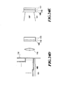
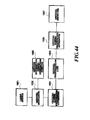
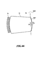
- Fig. 24 shows a modification in structure (Embodiment 5) of Fig. 20 and Fig. 21, Fig. 24A shows an example provided with both a phase filter 109a and an amplitude filter 109b for the spatial filter 109, the optical signal processing range is expanded by controlling both filters, rather than controlling one of the two filters, phase and amplitude.
- Fig. 24B shows an example which is the same in function as Fig. 21, but the Fresnel lens (kinoform) 108 is mounted on the upper surface of the filter, which is simple in fabrication.
- the focal length of the Fresnel lens (kinoform) 108 must be f/ns wherein ns is a refractive index of the slab waveguide 107.
- Fig. 24C shows an example in which a pattern mirror 114 serving as both the mirror 110 shown in Fig. 21 and the amplitude filter 109, which is simple in fabrication.
- Fig. 24D shows an example which, in place of the slab waveguide 107 and the Fresnel lens (kinoform) 108, is provided with a lens 115 only in this part, which has slightly larger in size but high precision Fourier transformation is possible.
- Fig. 24E shows an example provided with a phase filter 116 which serves as both the Fresnel lens 108 and the spatial filter (phase filter) 109. This construction is difficult in design but simple in fabrication.
- Embodiment 5 is described assuming the use of quartz waveguides, it is needless to say that the same optical circuit can be fabricated with semiconductor waveguides such as InP, GaAs, or Si, or dielectric material optical waveguide such as LiNbO 3 , or organic material optical waveguides such as polyimide.
- semiconductor optical waveguides are possible to construct even further compact apparatus due to their high refractive index, and an optical amplifier can be incorporated in the optical circuit.
- Fig. 25A shows an example in which the spatial filter shown in Fig. 21 is made from a liquid crystal
- 301a and 301b are transparent electrodes
- 302 is an alignment film
- 303 is a spacer
- 304 is a nematic liquid crystal
- 305 is a quarter-wave plate.
- the quarter-wave plate is necessary for eliminating polarization dependence when using a polarization- dependent spatial filter
- f axis and s axis of the quarter-wave plate are disposed with a 45-degree inclination to the waveguide facet(A-A' line in Fig.25A).
- Orientation of the liquid crystal is homogeneous orientation parallel or perpendicular to the waveguide facet(A-A' line in Fig.25A).
- Fig. 25B shows the structure of the transparent electrode 301a, which has strip-formed electrodes and the individual electrode can be applied with an optional voltage.
- a voltage orientation of crystal is changed, phase difference is changed between the transparent electrodes 301a and 301b, since the electrodes are provided in strips, a desired spatial phase filter can be achieved. That is, in this example, it is possible to make optical signal processing as necessary by adjusting the phase filter. Further, a twist nematic liquid crystal may be used as the liquid crystal. In this case, the quarter-wave plate is unnecessary.
- this arrangement functions as a polarization independent phase modulator.
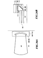
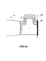
- Fig. 26 shows an embodiment 7 of the present invention, in which the optical path is bent to form an even smaller sized apparatus.
- 401 is a core of optical waveguide
- 402 is a mirror
- 403 is a groove on a slanted (7-8 degrees) end surface.
- an optical bend unit is formed of the groove 403 for bending light and the mirror 402 so that the focal plane of the slab waveguide 107 is on the mirror 110.
- the filter can be disposed on the quartz substrate, an even smaller sized apparatus can be constructed.
- the groove can be easily formed using a reactive ion etching apparatus.
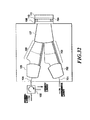
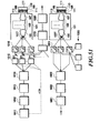
- Fig. 27 shows a transmission type structure, in which a first quartz substrate 101A having the first arrayed waveguide 106 and a second quartz substrate 101B having a second arrayed waveguide 505 are disposed on a heat sink 501.
- the two quartz substrates 101A and 101B are symmetrical in structure. That is, the quartz substrate 101A is integrated thereon with a first slab waveguide 105 for wave division, a first arrayed waveguide 106, and a second slab waveguide 107 for focusing, the second quartz substrate is also integrated thereon with a first slab waveguide 504, a second arrayed waveguide 505, and a second slab waveguide 506 for wave synthesis.
- a spatial filter and the like are disposed between the quartz substrates 101A and 101B.
- 502 denotes an optical amplifier.
- An arrayed waveguide grating 200A is formed on the quartz substrate 101A on the heat sink 501, and similarly a second arrayed waveguide grating 200B is formed on the quartz substrate 101B on the heat sink 501, disposed symmetrically about the spatial filter.
- the first arrayed waveguide grating 200A comprises an optical waveguide 104, a first slab waveguide 105, and arrayed waveguide 106, and a second slab waveguide 107.
- the other second arrayed waveguide grating 200B similarly comprise a first slab waveguide 504, an arrayed waveguide 505, a second slab waveguide 506, and an optical waveguide 507.
- Fig. 28 is an enlarged view, the spatial filter is one which is similar to that of Fig. 25, but since it is a transmission type, it is required to obtain at least a phase difference (2 ⁇ ). Further, the mirror 110 and the quarter-wave plate 305 of Fig. 25 are unnecessary and omitted. Since this construction has a polarization dependence, when eliminating the dependence, two stages of filters may be connected perpendicularly.
- the transmission type construction of the present embodiment is equivalent in operation to the construction shown in Fig. 20. While the apparatus becomes large, the circulator 102 of Fig. 20 is unnecessary and the loss can be reduced.
- 503 in Fig. 27 denotes a filter control unit.
- Fig. 29 shows a modification of the embodiment 8 shown in Figs. 27 and 28
- Fig. 27A is an example using a fixed spatial filter
- Fig. 29B is an example using the Fresnel lens (kinoform) 108 formed on the substrate
- Fig. 29C is an example using a phase filter 116 which serves as both Fresnel lens (kinoform) and phase filter
- Fig. 29D is an example using a lens 115 in place of the first slab waveguides 107 and 504.
- the spatial filter is transmission type, at least a phase difference of 2 ⁇ can be obtained.
- Fig. 30 shows another example of transmission type, in which phase adjustment is achieved by heating. That is, 601 is an arrayed waveguide, 602 is a heating electrode, 603 is a wiring, and 604 is a control unit.
- Fig. 31 shows an enlarged view of the arrayed waveguide.
- 605 is a groove provided in the waveguide
- 606 is a taper structure for reducing connection loss
- 607 is a half-wave plate.
- the groove 605, the taper 606, and the half-wave plate are a structure for reducing polarization dependence of the waveguide, which can also be used in other arrayed waveguide as necessary.
- phase of each waveguide of the arrayed waveguide 601 can be adjusted by adjusting the current in the electrode 602. That is, when it is disposed so that input end of the arrayed waveguide 601 is Fourier transformation plane by the slab waveguide 107, the arrayed waveguide 601, the heating electrode 602, the groove 605, the taper 606, and the half-wave plate 607 function as a variable phase filter.
- fabrication is made so that the phase difference between individual waveguides of the arrayed waveguide 601 is an integer multiple of 2 ⁇ . Also in the present embodiment, same as in the case of Fig. 25, optional phase variation and flexible optical signal are achieved.
- a construction is possible in which the spatial filter and the half-wave plate are disposed at the center to be connected to the phase adjustment arrayed waveguide end.
- Fig. 32 shows an example for hologram recording, in which 701 is a reference light input waveguide, 702 is a slab waveguide as distribution means, 703 is a second arrayed waveguide, and 704 is an optical recording medium.
- 704 a photo refractive crystal such as semiconductor MQW or barium titanate, a thermoplastic can be used.
- optical system 104-106 of the signal light is the same in construction as optical system 701-703 of the reference light.
- the signal light and reference light are Fourier transformed and undergo interference on the medium 704, and hologram recorded.
- phase conjugate light of signal light is output from the circulator 102. That is, the present embodiment has a function of recording high speed optical signal and generating phase conjugate light.
- Fig. 33 is another example of hologram recording, showing a transmission type.
- 801 is a slab waveguide as second focusing means
- 802 is an arrayed waveguide
- 803 is a slab waveguide as wave synthesis means
- 804 is an optical waveguide.
- signal light is input into the first waveguide 104 and reference light into the waveguide 701
- optical signal is hologram recorded on the waveguide 704.
- signal light is reproduced from the waveguide 804.
- a correlated signal between the two signal light can be output.
- Fig. 34 shows a waveform observation example of a very high speed optical signal, in which 901 is a CW light source of monochromatic light, 902 is an optical waveguide, 903 is a slab waveguide, and 904 is an optical receiver array.
- 901 is a CW light source of monochromatic light
- 902 is an optical waveguide
- 903 is a slab waveguide
- 904 is an optical receiver array.
- signal light is input into the waveguide 104 and reference light into the waveguide 701
- diffraction is made by hologram on the medium 704.
- temporal waveform is formed as a spatial optical amplitude distribution.
- An optical filter 906 is to set the wavelength of the CW light source to a wavelength different from signal light and control light to block input of signal light and reference light into the array 904.
- the slab waveguides 107 and 504 and the like as focusing means are to make the focal plane flat in combination with the Fresnel lens (kinoform), generally a large distortion occurs unless optical signal processing in frequency space is made on the focal plane, but the Fresnel lens and the like can be eliminated depending on the curvature of the focal plane.
- the spatial filter of phase filter or amplitude filter or both may be provided.
- the focal length of the Fresnel lens is equal to the focal length of the slab waveguide of the coupling means, however, it is not necessarily equal to each other, but can be determined according to whether dispersion is generated or dispersion compensation is made.
- the vertical direction bending means shown in Fig. 26B can be applied, for example, in Fig. 32, in this case, the spatial filter 109 and the mirror 110 shown in Fig. 26B are replaced with an optical recording medium.
- FIG. 35 An embodiment 13 of the present invention is shown in Fig. 35.
- the embodiment 13 is similar in basic structure to the apparatus of the embodiment 4, but differs in that an optical amplifier 120, an optical filter 121, and an optical amplifier 122 are provided at the light source side.
- Fig. 36 A detailed construction in the vicinity of the Fresnel lens is shown in Fig. 36.
- the reference numeral 111 indicates a quartz substrate
- 112 is a low reflection coating film
- 113 is a holding substrate.
- the Fresnel lens 108 can be fabricated by etching a material which is transparent in the operating wavelength region. Contour of the Fresnel lens is elliptical.
- the curvature of the Fresnel lens 108 in the minor axis direction is set to have a focal length of optical length of the lens surface and the end surface of the slab waveguide 107.
- the curvature in the major axis direction of the Fresnel lens 108 is set equal to the focal length of the slab waveguide 107.
- Signal light input into the optical fiber 103 is amplified by the optical amplifier 120, after removing unnecessary ASE light by the optical filter, passed through the circulator 121, and input into the optical waveguide 104. Then, the signal light is distributed by the first slab waveguide 105 to individual waveguides of the arrayed waveguide 106.
- the adjacent individual waveguides of the arrayed waveguide 106 differ in waveguide length by ⁇ L. Therefore, wherein n is a refractive index of the waveguide, adjacent waveguides have a phase difference of n ⁇ L. That is, the arrayed waveguide 106 has a wave division function same as a diffraction grating.
- the arrayed waveguide grating 200 comprising the first slab waveguide 105, the arrayed waveguide 106 and the second slab waveguide 107 has heretofore been used as a wavelength demultiplexer in a wavelength division multiplexing transmission apparatus.
- Output end of the arrayed waveguide 106 is connected to the second slab waveguide 107, and disposed on a circle of a radius f. That is, the second slab waveguide 107 functions as a lens having a focal length of f.
- Focal plane of the second slab waveguide 107 is located on a circle with the center at the output end of the arrayed waveguide 106 on the optical axis of the second slab waveguide 107.
- Optical signal processing in frequency space generally produces a large distortion unless carried out on the focal plane. Therefore, the Fresnel lens 108 is disposed at the output side of the slab waveguide 107. The focal plane is converted to a flat plane by the Fresnel lens 108. Focal length in the waveguide surface of the Fresnel lens 108 is set equal to f.
- Input light is passed through the spatial filter 109, reflected by the mirror 110, and again passed through the spatial filter 109.
- Figs. 37 and 38 show details of the spatial filter 109 and the Fresnel lens 108.
- the spatial filter 109 and the Fresnel lens can be fabricated by the same process. Thickness of the spatial filter 109 is equal to ⁇ 0 /(2n L ) because a maximum of phase difference 2 ⁇ is necessary in the forward and reverse directions in a reflection type, wherein ⁇ 0 is a tube center wavelength of the signal, and n L is a refractive index of the material of the spatial filter 109.
- the lens thickness is designed to have a focal length equal to the second slab waveguide 107 in order to convert the focal plane of the second slab waveguide 107 into a flat plane.
- the curvature in the direction (y) perpendicular to the waveguide substrate is set so that focal length in the quartz substrate 111 is equal to the thickness of the quartz substrate 11, in order to convert output light from the lens into parallel light.
- curvatures in x direction and y direction are Rx and Ry
- elliptical ring of the Fresnel lens 108 is shown by the following formula (1).
- m 1, 2, ....(integer) corresponds to discontinuity of the curved surface.
- R y R x x 2 m + y 2 m 2m ⁇ 0 n L
- the spatial filter 109 and the Fresnel lens 108 can be fabricated, for example, by exposing PMGI (PolyMethiGlutarImide) by means of an electron beam exposure apparatus, followed by developing.
- PMGI PolyMethiGlutarImide
- Fig. 39 shows a graph of exposure dependence of developing depth of PMGI.
- incident signal light is assumed as u(t), and a transmission function (forward and reverse) of the spatial filter 109 as h(x).
- f is time
- x is a position on the spatial filter 109.
- the signal light u(t) is divided by the arrayed waveguide 106, and focused at a different position x on the spatial filter 109.
- the reflected light is again passed through the arrayed waveguide 106 and inverse Fourier transformed.
- Figs. 41 and 42 show an example of filter characteristics of embodiment 13.
- characteristic of dispersion compensation filter for compensating a change in Fourier phase in the medium having a group velocity dispersion is ax 2 in the Fourier transformation plane.
- Fig. 41 and Fig. 42 correspond positive and negative of dispersion.
- FIG. 25A An embodiment 14 of the present invention will be described with reference to Fig. 25A, Fig. 25B, and Fig. 35.
- the spatial filter of the apparatus of the present embodiment is shown in Fig. 25A and Fig. 25B.
- Other parts are similar to those in the embodiment 1 shown in Fig. 35, and detailed description thereof is omitted.
- the quarter-wave plate is necessary, when using a spatial filter having a polarization dependence, for making it polarization independent.
- the liquid crystal can be homogeneously oriented parallel or perpendicular to the waveguide facet(A-A' line in Fig.25A).
- f axis and s axis of the quarter-wave plate 305 are slanted by 45 degrees to the waveguide surface.
- the transparent electrode 301-a is a strip-formed electrode, and each strip electrode can be applied with an optional voltage.
- a voltage is applied, orientation of the liquid crystal is changed, and phase difference between the transparent electrodes 301-a and 301-b. Since the electrode is provided in strips, a desired spatial phase filter can be achieved. That is, in the present embodiment, by adjusting the phase filter, it is possible to change the central wavelength of dispersion compensation, change the dispersion compensation amount, or make dispersion compensation according to the requirement.
- 200A is a first arrayed waveguide grating
- 200B is a second arrayed waveguide grating
- 501 is a heat sink
- 503 is a filter control unit
- 504 is a slab waveguide as second focusing means
- 505 is a second arrayed waveguide
- 506 is a slab waveguide as wave synthesis means
- 507 is a second optical waveguide.
- the optical waveguide 104, the first slab waveguide 105, the arrayed waveguide 106 and second slab waveguide 107; and the first slab waveguide 404, the arrayed waveguide 505, the second slab waveguide 506, and the optical waveguide 507 are symmetrical in construction.
- the spatial filter (Fig. 28) is a filter same as used in the embodiment 14, since it is a transmission type, it is required to obtain twice the phase difference (2 ⁇ ). Further, the mirror and the quarter-wave plate are omitted since they are unnecessary. Since this construction has a polarization dependence, to make it polarization independent, the filters for obtaining phase difference may be connected perpendicularly in two stages.
- the transmission type construction of the present embodiment is equivalent in operation to the reflection type construction shown in the embodiments 13 and 14.
- Fig. 44 shows an embodiment 16 of the present invention.
- 1001 is a light source
- 1002 is an optical modulator
- 1003 is an optical modulation signal generator
- 1004 is an optical signal processing apparatus as one of those shown in the embodiment 13 to embodiment 15
- 1005 is a transmission line comprising an optical fiber, and optical filter, an optical amplifier, and the like
- 1006 is an optical signal processing apparatus as one of those shown in the embodiment 13 to embodiment 15, and 1007 is an optical receiver.
- Self-phase modulation which is a major factor of signal degradation in the transmission line is generated nearly in proportion to the optical pulse peak power.
- the pulse width can be increased to reduce the peak power while maintaining the average power, thereby reducing the self-phase modulation.
- phase modulation is made in the optical signal processing apparatus 1004 to scramble the waveform to flatten the optical power, thereby reducing the peak power of the optical signal.
- Fig. 45 shows examples of a time waveform of modulator output optical amplitude and an output waveform after passing through the optical signal processing apparatus 1004.
- Dispersion in the transmission line is mainly a group velocity dispersion of the third term of the formula (3) which is a square term with respect to the frequency.
- phase filter characteristic is adapted to generate dispersion of the same sign as the dispersion of the transmission line for the square term. Or, tertiary or higher term is used, or a filter having a quite random phase changes is used.
- phase filter of the reception side optical signal processing apparatus is designed to compensate dispersion by the transmission line and phase scramble previously given by the optical signal processing apparatus 1004.
- signal light output from the optical modulator 1002 is assumed as u(t), phase filter characteristic of the optical signal processing apparatus (forward and reverse for reflection type) as h 1 ( ⁇ (x)), Fourier transformation as H 1 (t)), and waveform distortion generated by dispersion of the transmission line as J(t), signal light s(t) incident to the optical signal processing apparatus 1006 is approximated by the following formula (7), wherein * means convolution.
- s (t) u (t) * H 1 (t) * J (t)
- phase filter characteristics of the optical signal processing apparatus 506 may be set as the following formula (8).
- h 2 ( ⁇ (x)) h 1 ( ⁇ (x)) 2 •j ⁇ ( ⁇ (x)) 2 h 1 ( ⁇ (x)) 2 j ⁇ ( ⁇ (x)) 2
- the optical signal processing apparatus 504 emphasizes low s/N frequency signal using an amplitude filter and makes transmission, a phase filter for compensating dispersion of the transmission line at the receiver side, and an amplitude filter having the reverse characteristics to the transmission side are used to equalize S/N with respect to the frequency, thereby enhancing the receiver sensitivity.
- a filter for reducing only the vicinity of the central frequency is used as the amplitude filter of the receiver side optical signal processing apparatus 1006 to attenuate the low frequency component of time waveform, and interference between codes generated due to nonlinear effect and the like is reduced, thereby enhancing the reception sensitivity. Characteristics of such an amplitude filter are shown in Fig. 48.
- phase filter of an embodiment 17 of the present invention Characteristics of phase filter of an embodiment 17 of the present invention is shown in Fig. 49A and Fig. 49B for reflection type configuration. Configuration other than the filter is the same as the embodiments 13 to 14.
- Input signal light is assumed to be an amplitude modulated signal light.
- Spectral amplitude of the amplitude modulated signal is shown in Fig. 50A and Fig. 50B. There are side bands above and below the carrier frequency.
- spectral amplitude of angular modulated signal light has the shape as shown in Fig. 20B. A difference from the frequency spectral amplitude of amplitude modulation is that the upper and lower side bands are reverse in phase.
- FIG. 51 An embodiment 18 of the present invention is shown.
- 1011 is a short pulse light source
- 1012 is an optical amplifier
- 1013 is an optical wavelength filter
- 1014 is an optical splitter
- 1015 is n units of optical modulation circuits
- 1016 is n units of optical circulators
- 1017 is n units of input waveguides
- 1018 is an optical combiner
- 1019 is an optical amplifier
- 1020 is an optical transmission line
- 1021 is an optical amplifier
- 1022 is an optical wavelength filter
- 1023 is an optical splitter
- 1024 is n units of optical circulators
- 1025 is n units of optical receiver circuits.
- This arrangement differs from the above described embodiment 17 in that the present embodiment mainly makes multiplexing of optical signal.
- optical band width is mainly determined by the pulse width.
- the band width can be efficiently utilized.
- the pulse is divided into n units of modulation circuit to achieve modulation.
- each modulation signal is differently phase modulated in frequency regions, and synthesized and multiplexed.
- phase modulation for example, different or shifted PN (Pseudorandom Noise) sequence or M (Maximum Length code) sequence may be used.
- PN Physical Random Noise
- M Maximum Length code
- spatial filter phase is changed in relative phase of [0, ⁇ /2] according to [1, 0] of the sequence.
- FIG. 52 An envelope of average optical amplitude distribution on the filter plane is shown in Fig. 52.
- the envelope of optical intensity distributions corresponding to k-1, k, and k+1'th channel are separated at intervals equal to the interval din at the connection of the input optical waveguide to the slab waveguide 105.
- phase modulated light is waveguided by the optical circulator 1016 to the optical synthesis device 1018.
- each divided signal is demodulated in the frequency region using a spatial filter which is phase conjugate with the transmission side optical signal processing apparatus.
- the receiver circuit is required to have a high performance for sufficiently responding the pulse.
- a nonlinear device For very high speed discrimination, a nonlinear device, a nonlinear optical receiver, or a high speed opto-electric conversion device and a flip-flop circuit is used.
- Fig. 53 shows waveforms of modulation signal, after phase modulation, and demodulated signal after reproduction. That is, the present embodiment functions as a spectrum spread transmission apparatus in the optical frequency region. Since, as the number of multiplexing increases, it becomes difficult to reduce correlation of phase modulation for all combinations, background noise increases, and multiplexing becomes difficult, however, it is possible to utilize a band width corresponding to the pulse width with an efficiency of about 50%.
- FIG. 54 An embodiment 19 of the present invention is shown.
- 1031 is a short pulse light source
- 1032 is an optical amplifier
- 1033 is an optical splitter
- 1034 is an optical division device
- 1035 is n units of optical modulation circuits
- 1036, 1037, and 109 are the same transmission type optical signal processing apparatus as shown in Fig. 43, increasing the input/output waveguides to n units
- 1038 is an optical combiner
- 1039 is an optical amplifier
- 1040 is an optical transmission line
- 1041 is an optical amplifier
- 1042 is an optical wavelength filter
- 1043 is an optical splitter
- 1044, 1045, and 109 are the same transmission type optical signal processing apparatus as shown in Fig. 43 as described above
- 1046 is n units of optical receiver circuits.
- the embodiment 18 is constructed with a transmission type phase modulation circuit, and the operation is the same as the embodiment 18.
- Fig. 55 shows an embodiment 20 of the present invention, which is a short pulse light source.
- the short pulse light source according to the present invention comprises an optical modulator 2011, a drive circuit 2012 for driving the optical modulator 1011, an optical gain medium 2013, an pumping circuit 2014 for forming population inversion on the optical gain medium 2013, an arrayed waveguide grating 2015 with eliminated the input waveguide 71 from the arrayed waveguide grating 62 shown in Fig. 5, optical coupling means 2016 for coupling the optical modulator (optical modulation means) 2011 and the optical gain medium (optical gain means) 2013, and optical coupling means 2017 for coupling the optical gain medium 2013 and the arrayed waveguide grating 2015.
- the optical coupling means 2016 side of the optical modulator 2011 is provided with a low reflection coating 2018, and a high reflection mirror 2019 is disposed at the opposite side (outside).
- the optical coupling means 2017 side of the arrayed waveguide grating 2015 is provided with a low reflection coating 2020, and a high reflection mirror 2021 is disposed at the opposite side (outside).
- the optical modulator 2011 can be an MQW modulator, an LN modulator, or the like.
- the optical gain medium 2013 can be a traveling wave type semiconductor optical amplifier, rare earth doped optical fiber amplifier, or the like.
- the pumping circuit 1014 is a current source when the optical gain medium 1013 is a traveling wave type semiconductor optical amplifier, and an pumping light source for the case of the rare earth doped optical fiber amplifier.
- the substrate 70 of the arrayed waveguide grating 2015 can be a semiconductor substrate such as InP or GaAs in addition to quartz substrate.
- the arrayed waveguide grating 2015 comprises a slab waveguide 72, an arrayed waveguide 73 comprising a plurality of waveguides gradually increasing in length by waveguide length difference ⁇ L, a slab waveguide 74, and a plurality of output waveguides, formed on the substrate 70.
- ns is a refractive index of the slab waveguides 72 and 74
- nc is a refractive index of the arrayed waveguide 73
- d is a spacing of the arrayed waveguide 73 on the slab waveguide end surface
- ⁇ is a focusing direction with respect to the central axis of the slab waveguide 74
- f s is a focal length
- ⁇ is wavelength of light
- the reflection spectrum of such an arrayed waveguide grating 2015 is according to the interval ⁇ x and the core width of the output waveguide 75.
- a reflection spectrum when ⁇ x is 50 ⁇ m and the core width is 10 ⁇ m is shown in Fig. 57.
- a comb-formed reflection spectrum having reflection peaks at every 50 GHz is obtained.
- an optical resonator is formed between the high reflection mirror 2017 and the high reflection mirror 2021, thereby simultaneously oscillating light of a plurality of wavelengths when the gain of the optical gain medium is sufficiently high.
- phase relation of each vertical mode is maintained constant, an optical short pulse sequence of a repetition frequency f is generated.
- the oscillation spectrum is shown in Fig. 58 and the oscillation pulse waveform is shown in Fig. 59.
- the prior art mode locked type laser has been difficult to set the frequency of each mode.
- frequency of each mode is determined by the interval ⁇ x of the output waveguide 75 of the arrayed waveguide grating 2015, frequency of each mode can be set in detail. Further, when the arrayed waveguide grating 2015 is formed on a quartz substrate, oscillation is possible at a frequency stable to temperature changes.
- the prior art mode locked laser has been difficult to set the pulse width.
- the pulse width can be previously set. For example, a Gaussian type envelope spectrum as shown in Fig. 60 can be achieved.
- the pulse waveform on the time base is also Gaussian type.
- Fig. 61 shows an embodiment 21 of the present invention, which is a short pulse light source.
- the basic structure is the same as the embodiment 20 shown in Fig. 55.
- an enlarged view of the slab waveguide 74 and the output waveguide 75 part of the arrayed waveguide grating 2018 is shown.
- the present embodiment is characterized in that lengths of individual waveguides of the output waveguide 75 are changed so that dispersion in the optical resonator can be compensated.
- a semiconductor material has a large dispersion
- most of dispersion in the optical resonator of the present invention is considered to be semiconductor material dispersion in the optical modulator 2011 and the optical gain medium 2013.
- the dispersion is about 0.005 ps/nm.
- adjacent waveguide length difference can be set as follows; 0.4 ⁇ m ⁇ m ⁇ k /2n eff wherein ⁇ k is the wavelength of k's mode and n eff is the effective refractive index of the output waveguide.
- Fig. 62 shows an embodiment 22 of the present invention, which is a short pulse optical light source.
- the basic structure is the same as the embodiment 20 shown in Fig. 55.
- an enlarged view of the output waveguide 75 part of the arrayed waveguide grating 2015 in the embodiment 20 is shown.
- the present embodiment is characterized by a lens array and a liquid crystal spatial modulator having a high reflection mirror on one side in place of the high reflection mirror 2021 at the end surface of the output waveguide 75.
- the lens array comprises a gradient refractive index lens 2022 disposed at spacings of ⁇ x.
- the liquid crystal spatial modulator comprises a polarizer plate 2023, a glass substrate 2024-1, a twist nematic liquid crystal 2027 placed between a transparent electrode 2025 and a polarizer plate 2026 disposed at a spacing of ⁇ x, a high reflection mirror 2028, and a glass substrate 2024-2, which are stacked. End surface of the output waveguide 75, and both surfaces of the gradient refractive index lens 2022 and the polarization plate 2023 are provided with a low reflection coating 2029.
- the liquid crystal spatial modulator can control the reflectivity from the high reflection mirror 2028 to the output waveguide 75 by applying a voltage between opposing transparent electrode 2025. This enables mode control dynamically, and can change the pulse waveform as necessary.
- the spatial modulator in this case is not limit to the liquid crystal spatial modulator, but another modulator such as an MQW modulator, a modulator by Franz-Keldysh effect, an LN modulator, or a modulator by a nonlinear material can be utilized.
- 74 is a slab waveguide
- 2024 is a holding substrate
- 2028 is a high reflection mirror
- 3000 is a dispersion compensation phase filter.
- Fig. 63 shows an embodiment 23 of the present invention (short pulse light source).
- the present embodiment is characterized in that a diffraction grating 2030 is formed in the output waveguide instead of using the high reflection mirror 2021.
- This diffraction grating 2030 can be functioned as a very narrow band high reflection mirror. Since it has a spectroscopic characteristic, it enables very detailed mode wavelength setting. Further, by disposing the diffraction grating at an appropriate position, dispersion compensation in the optical resonator is possible as in the embodiment 20, and can generate a pulse close to the transform limit.
- Fig. 64 shows an embodiment 24 of the present invention (short pulse light source).
- the present embodiment is characterized in that two or three or more units of the output waveguides provided with the diffraction grating 2030 as in the embodiment 22 are connected to an optical coupler 2031.
- an optical coupler 2031 By coupling light from the predetermined waveguides of the output waveguide 75 by the optical coupler 2031, it is possible to couple a predetermined mode when mode locked oscillation is being made, thereby generating various pulse waveforms. For example, when coupling only an odd or even numbered mode to be output, an optical short pulse sequence of twice the repetition frequency of mode locked frequency can be generated.
- Fig. 65 shows an embodiment 25 of the present invention (short pulse light source).
- an arrayed waveguide grating 2032 has a construction in which the output waveguide 75 is eliminated from the arrayed waveguide grating 2015 in the embodiment 20, and a plurality of high reflection mirrors 2021 are disposed at spacings of ⁇ x on the focal plane of the slab waveguide 74.
- Other construction is the same as the embodiment 20.
- Fig. 66 shows an enlarged view of the slab waveguide 74 part of the arrayed waveguide grating 2032.
- end surface of the substrate 70 of the arrayed waveguide grating 2032 is cut along the focal plane of the slab waveguide 74, and a plurality of high reflection mirrors 2021 are disposed at spacings of ⁇ x on the end surface. Further, to reduce end surface reflection from parts other than the high reflection mirrors 2021, the entire end surface of the substrate 70 is provided with a low reflection coating.
- Fig. 67 shows an embodiment 26 of the present invention (short pulse light source).
- the present embodiment is characterized in that a diffraction grating 2033 is formed on the focal plane of the slab waveguide 74 instead of using the high reflection mirror 2021.
- the diffraction grating can be written by using ultraviolet light as in a diffraction grating formed in an optical fiber. Since a quartz substrate is small in coupling constant of diffraction grating and small in loss, the diffraction grating can be functioned as a very narrow band high reflection mirror. Further, in addition to the spectroscopic function of the arrayed waveguide grating, since the high reflection mirror by the diffraction grating 2033 in the slab waveguide 74 has a spectroscopic characteristic, a very detailed mode wavelength can be set. Still further, by dislocating individual positions of the diffraction grating 2033 on the normal line of the focal plane, dispersion compensation in the optical resonator as in the embodiment 20, thereby generating a pulse close to the transform limit.
- Fig. 68 shows an embodiment 27 of the present invention (short pulse light source).
- Fig. 68A is a plan view
- Fig. 68B is a cross sectional view of Fig. 68A along line A-A'.
- the reference numeral 76 indicates a waveguide core.
- the present embodiment is characterized in that, instead of using the high reflection mirror 2021, a groove 2034 perpendicular to the substrate 70 is formed along the focal plane of the slab waveguide 74, and a polyimide film 2036 formed with a plurality of mirrors 2035 is inserted in the groove.
- the polyimide film 2036 to eliminate unnecessary reflected light from the waveguide end surface, is fixed with an adhesive which is transparent in the operating wavelength and small in refractive index difference from the equivalent refractive index of the waveguide. Further, to eliminate reflected light from part without the mirror 2035 of the polyimide film 2036, the surface is provided with a low reflection coating 2038. Still further, to avoid reflection from the back surface, the back side is laminated with a light absorption film 2039. Yet further, in the present embodiment, various films can be used other than polyimide film.
- the arrayed waveguide gratings in the embodiments 20 to 26 are set in a short pulse light source, the arrayed waveguide grating of these embodiments can also be applied in other applications such as waveform shaping and dispersion compensation
- Fig. 69 shows an embodiment 28 of the present invention (short pulse light source).
- the present embodiment shows a construction in which the optical modulator 2011 and the optical gain medium 2013 are integrated.
- An n-InP substrate 2040 is stacked with an optical modulation MQW layer 2041, an i-etch stop layer 2042, a laser MQW layer 2043, an n-InP layer 2044, an n-InGaAsP layer 2045, and an AuZnNi electrode 2046, and an AuGeNi electrode 2047 is mounted on the backside of the n-InP layer 2040.
- End surface at the optical modulator 2011 side is provide with a high reflection mirror 2048 (2019), and end surface of the optical gain medium 2013 is provided with a low reflection coating 2049.
- Fig. 70 2011 is a fiber output type optical modulator provided with a low reflection structure at the output surface and with a high reflection structure on the opposite surface
- 2102 is a modulator drive circuit
- 2103 is a fiber output type optical gain medium
- 2104 is a gain medium pumping circuit
- 2105 is a 4-terminal type optical circulator
- 2106 is a non-reflection terminator
- 2107 is an optical coupler
- 2108 is a polarization maintaining optical fiber
- 2109 is an arrayed waveguide grating
- 2110 is an optical waveguide
- 2111 is a first slab waveguide
- 2112 is a waveguide array
- 2113 is a second slab waveguide
- 2114 is a lens
- 2115 is a high reflection mirror
- 2116 is a fine movement table.
- Fig. 71A is a structural plan view
- Fig. 71B is an end surface view
- 2117 is a quartz substrate
- 2118 is a point reflection coating
- 2119 is a high reflection mirror such as Au/Cr.
- Each mirror is constant in width, adapted to change the adjacent mirror spacing in y-direction of Fig. 71A.
- Fig. 72 shows layout in the vicinity of the mirror 2115.
- 2120 is a lens substrate
- 2114 is a lens, having a function to convert the cylindrical focusing plane of 2109 into a flat plane.
- the surface having the mirror 2115 is disposed to be in line with the focusing plane.
- a direction vertical to the paper surface is y-direction
- rotation angle about the y-axis is ⁇ .
- the fine movement table 2116 connected to the mirror 2115 the mirror can be finely moved in the x and y-directions and ⁇ -direction.
- central frequency during mode locked oscillation and oscillation frequency of each mode can be controlled.
- mode interval that is, repetition period of the pulse
- the ⁇ -direction is controlled so that the delay time in the resonator is an integer multiple or inverse thereof of the repetition period of the pulse.
- the present embodiment 29 is characterized in that the repetition period and central frequency of the pulse sequence can be easily controlled. While individual parts are shown to be connected to the optical fiber, it is needless to say that they may be connected to the lens as in other embodiments. Further, in other embodiments, the parts may be connected to the optical fiber as in the present embodiment.
- Fig. 73 shows an embodiment 30 of the present invention.
- the present embodiment relates to an optical signal processing apparatus which can provide observation of real-time waveform of optical signal.
- 3101 is a signal light input waveguide for inputting signal light.
- 3102 is a slab waveguide, which has a function to distribute output light of the signal light input waveguide to an arrayed waveguide 3103.
- the arrayed waveguide 3103 has a function for time - space conversion of incident signal light.
- 3104 is a reference light input waveguide for inputting reference light.
- 3105 is a first slab waveguide for the reference light, and has a function of distributing the output light of the reference light input waveguide 3104 to an arrayed waveguide 3106.
- the arrayed waveguide 3106 has a function of time - space conversion of incident reference light.
- 3107 is a second slab waveguide, which has a function of Fourier transformation of output light individually from the arrayed waveguide 3103 and the arrayed waveguide 3106.
- 3108 is an photo diode (PD) array, which detects electrical field amplitude distribution of Fourier transform hologram formed on the focal plane of the second slab waveguide 3107 by interference of the signal light Fourier transformed by the second slab waveguide 3107 with the reference light.
- 3109 is an optical signal restoration circuit for restoring the input signal light from the electrical field strength distribution of the Fourier transformed hologram detected by the PD array 3108.
- 200 is an arrayed waveguide grating comprising the waveguides 3101 and 3104, the slab waveguides 3102, 3105, and 3107, and the arrayed waveguides 3103 and 3106.
- the two arrayed waveguides 3103 and 3106 are bent in the same direction as shown in Fig. 73, thereby aligning the sign of the spatial base to the time base on the output surface of the arrayed waveguides.
- a lens may further be provided on the focal plane of the second slab waveguide 107 to make phase compensation.
- the signal light arrayed waveguide 3103 is provided at the output side
- the reference light arrayed waveguide is provided at the input side individually with a straight arrayed waveguide of about 1 cm, thereby preventing the arrayed waveguides from being overlapped with each other.
- a construction shown in Fig. 73B is also possible.
- 3110 is a second slab waveguide for reference light
- 3111 is a half mirror.
- the half mirror 3111 is introduced, after forming the waveguide, by forming a groove in the substrate by a dicing saw and inserting.
- the position of the half mirror is determined so that reference light incident to the slab waveguide 3110 is reflected at the half mirror 3111, and focused on the focal plane of the slab waveguide 3107.
- the optical axis of the reference light is required to be set in an angle of 3 to 30 degrees with respect to the optical axis of signal light.
- the waveguide in Fig. 73 is formed as an example as shown below.
- a lower clad layer and a core layer are stacked in this order by a flame hydrolysis decomposition method (FHD method) on a single crystal silicon substrate, heated to a high temperature in an annealing furnace to form a transparent glass film covering the silicon substrate.
- FHD method flame hydrolysis decomposition method
- patterning is made to the shape of waveguide, unnecessary core layer is removed by dry etching, an upper clad layer is again stacked using the FHD method, and heated to a high temperature to make the upper clad layer transparent.
- a semiconductor waveguide structure fabricated by epitaxial growing of semiconductor higher in refractive index than a clad of InGaAsP as a core layer of a semiconductor layer such as of InP, after patterning and etching, again growing InP as an upper clad layer has the same function.
- the materials are transparent in the operating wavelength region.
- a detailed view of the photo diode array used in the present embodiment is shown in Fig. 73D.
- the size of one piece of the photo diode in 256 units of single dimensional array is 200 ⁇ m in length and 30 ⁇ m in width, and individual pixels are arranged in a period of 50 ⁇ m. Electrical charge generated in each pixel is accumulated in the charge integrator 3114. The accumulated charge is read by sequentially operating the pixels by the CMOS shift register 3115.
- the optical signal restoration circuit 3109 comprises a computer and hologram for making mathematical operation, which will be described later, on the distribution of hologram interference pattern detected by the photo diode array, and a display device for displaying the electrical field distribution of the restored original optical signal.
- signal light s 1 (t) to be observed is input in the waveguide 3101, and known reference light r 1 (t) is input in the waveguide 3104, at the output ends of the individual waveguides 3103 and 3106, when the coordinate axis is x 1 , the signal light and the reference light are time - space converted individually into s 2 (x 1 ) and r 2 (x 1 ).
- These optical signals s 2 (x 1 ) and r 2 (x 1 ) are Fourier transformed by diffraction during transmitting the waveguide 3107, the signal light and reference light are converted individually into S( ⁇ ) and R( ⁇ ), wherein ⁇ is a spatial frequency axis in the focal plane coordinates.
- S*( ⁇ ) and R*( ⁇ ) individually represent complex conjugate of S( ⁇ ) and R( ⁇ ).
- G( ⁇ ) ⁇ R( ⁇ )/ R( ⁇ ) 2 ( S( ⁇ ) 2 / R( ⁇ ) 2+1 ) ⁇ R( ⁇ ) + S( ⁇ ) + S*( ⁇ ) ⁇ ⁇ R( ⁇ ) ⁇ 2 / R( ⁇ ) 2 can be derived.
- G( ⁇ ) ⁇ R( ⁇ )/ R( ⁇ ) 2 ( S( ⁇ ) 2 / R( ⁇ ) 2+1 ) ⁇ R( ⁇ ) + S( ⁇ ) + S*( ⁇ ) ⁇ ⁇ R( ⁇ ) ⁇ 2 / R( ⁇ ) 2 can be derived.
- the formula (2) since, in the slab waveguide 3107, signal light s 2 (x 1 ) and reference light r 2 (x 1 ) are applied from different positions, this is a construction equivalent to off-axis method in the holography.
- the focal plane of the second slab waveguide 3107 is an arc, however, in the present embodiment, it is cut on a straight line in the vicinity of the focal plane, the focal plane and the cut surface are not strictly in line with each other. That is, the time - spatially changed signal light is not a strict Fourier transformation image on the straight cut plane. Therefore, when the original signal waveform is reproduced from hologram interference pattern received by the photo diode array, an error occurs at the time of making inverse Fourier transformation.
- a compensation is made by sticking a Fresnel lens for compensating dispersion due to a phase shift on the cut surface of the second slab waveguide 3107, however, when reproducing the waveform of the signal light by the calculation as described above, even without the Fresnel lens, it is also possible to make correction by compensating the dispersion due to the phase shift to make calculation of diffraction light, using more common diffraction formula, rather than Fourier transformation in the process of calculating the diffraction by the lens, that is, in the process of making inverse Fourier transformation.
- Fig. 74 shows an embodiment 31 of the present invention, which relates to a waveform observable optical signal processing apparatus.
- 3201 is a diffraction grating, which has a function of time - space converting input signal light 3204 and input reference light 3205.
- 3202 is a lens, which has a function of Fourier transforming the signal light and reference light diffracted by the diffraction grating 3201.
- 3203 is an photo diode (PD) array disposed in the vicinity of the focal plane of the lens 3202, for detecting electrical field strength distribution of the Fourier transform hologram formed on the focal plane of the lens 3202 by interference of the Fourier-transform signal light and reference light.
- PD photo diode
- 3206 is an optical restoration circuit for restoring the input signal light from the electrical field strength distribution of the Fourier-transform hologram detected by the PD array 3203. Similarly to the embodiment 30, it is possible to derive the signal light by mathematical operation from the Fourier-transform hologram of the off-axis method.
- the present invention relates to an optical signal processing apparatus and optical signal processing method which enable generation, waveform shaping, waveform measurement, waveform recording, correlation processing, and the like of optical pulses of 1-10 ps.
- a basic construction of the optical signal processing apparatus includes an optical waveguide (9), (13), (22), (26), (33), (37), (41), (56), a first means (2), (10), (14), (25), (36), (42), (57) for equally distributing output light of the optical waveguide, an optical waveguide comprising an aggregate of optical waveguides changing in optical length by a constant interval, an arrayed waveguide (3), (11), (15), (24), (32), (43), (58) for dividing the output light, second means (4), (12), (16), (23), (34), (35), (59) for focusing optical output of the arrayed waveguide, and a mirror (110), (402), (2021), (2048), (2115) for receiving and reflecting incident light focused by the second means.
- the apparatus includes an optical waveguide, first means for equally distributing output light of the optical waveguide, an arrayed waveguide comprising an aggregate of optical waveguides changing in optical length by a constant interval for dividing the output light, second means for focusing optical output of the arrayed waveguide, and a spatial filter (5), (17), (109) for receiving light focused by the second means to distribute the incident light on a straight line and making desired amplitude or phase modulation of the light according to the position on the straight line and reflecting the light.
Applications Claiming Priority (11)
| Application Number | Priority Date | Filing Date | Title |
|---|---|---|---|
| JP23167396 | 1996-09-02 | ||
| JP23167396 | 1996-09-02 | ||
| JP28695596 | 1996-10-29 | ||
| JP28695596 | 1996-10-29 | ||
| JP4392197 | 1997-02-27 | ||
| JP4392197 | 1997-02-27 | ||
| JP5887797 | 1997-03-13 | ||
| JP5887797 | 1997-03-13 | ||
| JP17946997 | 1997-07-04 | ||
| JP17946997 | 1997-07-04 | ||
| EP97115119A EP0826989B1 (fr) | 1996-09-02 | 1997-09-01 | Dispositif de traitement de signaux optiques et méthode de traitement de signaux optiques |
Related Parent Applications (1)
| Application Number | Title | Priority Date | Filing Date |
|---|---|---|---|
| EP97115119A Division EP0826989B1 (fr) | 1996-09-02 | 1997-09-01 | Dispositif de traitement de signaux optiques et méthode de traitement de signaux optiques |
Publications (2)
| Publication Number | Publication Date |
|---|---|
| EP1452894A2 true EP1452894A2 (fr) | 2004-09-01 |
| EP1452894A3 EP1452894A3 (fr) | 2005-02-09 |
Family
ID=27522349
Family Applications (5)
| Application Number | Title | Priority Date | Filing Date |
|---|---|---|---|
| EP04012362A Expired - Lifetime EP1452895B1 (fr) | 1996-09-02 | 1997-09-01 | Dispositif de traitement de signaux optiques et méthode de traitement de signaux optiques |
| EP97115119A Expired - Lifetime EP0826989B1 (fr) | 1996-09-02 | 1997-09-01 | Dispositif de traitement de signaux optiques et méthode de traitement de signaux optiques |
| EP04012363A Expired - Lifetime EP1452896B1 (fr) | 1996-09-02 | 1997-09-01 | Dispositif de traitement de signaux optiques et méthode de traitement de signaux optiques |
| EP04012361A Withdrawn EP1452894A3 (fr) | 1996-09-02 | 1997-09-01 | Dispositif de traitement de signaux optiques et méthode de traitement de signaux optiques |
| EP04012364A Withdrawn EP1452897A3 (fr) | 1996-09-02 | 1997-09-01 | Dispositif de traitement de signaux optiques et méthode de traitement de signaux optiques |
Family Applications Before (3)
| Application Number | Title | Priority Date | Filing Date |
|---|---|---|---|
| EP04012362A Expired - Lifetime EP1452895B1 (fr) | 1996-09-02 | 1997-09-01 | Dispositif de traitement de signaux optiques et méthode de traitement de signaux optiques |
| EP97115119A Expired - Lifetime EP0826989B1 (fr) | 1996-09-02 | 1997-09-01 | Dispositif de traitement de signaux optiques et méthode de traitement de signaux optiques |
| EP04012363A Expired - Lifetime EP1452896B1 (fr) | 1996-09-02 | 1997-09-01 | Dispositif de traitement de signaux optiques et méthode de traitement de signaux optiques |
Family Applications After (1)
| Application Number | Title | Priority Date | Filing Date |
|---|---|---|---|
| EP04012364A Withdrawn EP1452897A3 (fr) | 1996-09-02 | 1997-09-01 | Dispositif de traitement de signaux optiques et méthode de traitement de signaux optiques |
Country Status (3)
| Country | Link |
|---|---|
| US (2) | US6122419A (fr) |
| EP (5) | EP1452895B1 (fr) |
| DE (3) | DE69739680D1 (fr) |
Families Citing this family (78)
| Publication number | Priority date | Publication date | Assignee | Title |
|---|---|---|---|---|
| US5926587A (en) * | 1997-09-08 | 1999-07-20 | Lucent Technologies Inc. | Optical passband filters |
| US6111996A (en) | 1998-03-13 | 2000-08-29 | Northern Telecom Limited | Optical multiplexer/demultiplexer |
| EP0936482A3 (fr) * | 1998-02-13 | 2002-09-25 | Nortel Networks Limited | Multiplexeur/Démultiplexeur optique |
| US6141467A (en) * | 1998-03-18 | 2000-10-31 | Lucent Technologies Inc. | Wavelength-division-multiplexing programmable add/drop using interleave-chirped waveguide grating router |
| JP3566096B2 (ja) * | 1998-08-31 | 2004-09-15 | 富士通株式会社 | 位相共役変換及び波長変換のための装置 |
| KR100280822B1 (ko) * | 1998-12-03 | 2001-03-02 | 정선종 | 광섬유 모드 록킹 레이저 |
| KR100322125B1 (ko) * | 1999-01-14 | 2002-02-04 | 윤종용 | 배열격자도파로 모듈 및 이를 이용한 광신호 모니터링 장치 |
| US6563620B1 (en) * | 1999-01-25 | 2003-05-13 | Massachusetts Institute Of Technology | Quasi-dispersionless optical fiber transmission, dispersion compensation and optical clock |
| US7127172B1 (en) * | 1999-06-02 | 2006-10-24 | Massachusetts Institute Of Technology | Optical frequency filter |
| US6275623B1 (en) | 1999-07-12 | 2001-08-14 | Corning Incorporated | Dynamically configurable spectral filter |
| JP3432457B2 (ja) * | 1999-07-29 | 2003-08-04 | 日本電信電話株式会社 | 波長可変光源、波長変換装置、および波長ルータ |
| JP3346751B2 (ja) * | 1999-10-14 | 2002-11-18 | 日本電気株式会社 | アレイ導波路格子 |
| US6301409B1 (en) * | 1999-12-23 | 2001-10-09 | Nortel Networks Limited | Optical comb filter |
| US6724783B2 (en) * | 2000-04-14 | 2004-04-20 | The Regents Of The University Of California | Method and apparatus for arbitrary waveform generation using photonics |
| US6574397B2 (en) * | 2000-12-29 | 2003-06-03 | Sumitomo Electric Industries, Ltd. | Optical multiplexer/demultiplexer |
| US7567596B2 (en) | 2001-01-30 | 2009-07-28 | Board Of Trustees Of Michigan State University | Control system and apparatus for use with ultra-fast laser |
| US7583710B2 (en) | 2001-01-30 | 2009-09-01 | Board Of Trustees Operating Michigan State University | Laser and environmental monitoring system |
| US7450618B2 (en) | 2001-01-30 | 2008-11-11 | Board Of Trustees Operating Michigan State University | Laser system using ultrashort laser pulses |
| US8208505B2 (en) | 2001-01-30 | 2012-06-26 | Board Of Trustees Of Michigan State University | Laser system employing harmonic generation |
| US6574396B1 (en) * | 2001-03-12 | 2003-06-03 | Lucent Technologies Inc. | Waveguide grating arrangement using a segmented reflector |
| RU2197783C2 (ru) * | 2001-03-15 | 2003-01-27 | Аджалов Владимир Исфандеярович | Способ организации доступа к сетям передачи пакетов данных |
| GB0107112D0 (en) * | 2001-03-21 | 2001-05-09 | Bookham Technology Plc | Optical demultiplexer |
| US6526187B1 (en) | 2001-05-17 | 2003-02-25 | Optronx, Inc. | Polarization control apparatus and associated method |
| US6690844B2 (en) | 2001-05-17 | 2004-02-10 | Optronx, Inc. | Optical fiber apparatus and associated method |
| US6891685B2 (en) * | 2001-05-17 | 2005-05-10 | Sioptical, Inc. | Anisotropic etching of optical components |
| US6603889B2 (en) | 2001-05-17 | 2003-08-05 | Optronx, Inc. | Optical deflector apparatus and associated method |
| US6608945B2 (en) | 2001-05-17 | 2003-08-19 | Optronx, Inc. | Self-aligning modulator method and associated apparatus |
| US6748125B2 (en) | 2001-05-17 | 2004-06-08 | Sioptical, Inc. | Electronic semiconductor control of light in optical waveguide |
| US6947615B2 (en) | 2001-05-17 | 2005-09-20 | Sioptical, Inc. | Optical lens apparatus and associated method |
| US6625348B2 (en) | 2001-05-17 | 2003-09-23 | Optron X, Inc. | Programmable delay generator apparatus and associated method |
| US6912330B2 (en) | 2001-05-17 | 2005-06-28 | Sioptical Inc. | Integrated optical/electronic circuits and associated methods of simultaneous generation thereof |
| US6654511B2 (en) | 2001-05-17 | 2003-11-25 | Sioptical, Inc. | Optical modulator apparatus and associated method |
| US6493502B1 (en) | 2001-05-17 | 2002-12-10 | Optronx, Inc. | Dynamic gain equalizer method and associated apparatus |
| GB0118637D0 (en) * | 2001-07-31 | 2001-09-19 | Bookham Technology Plc | Integrated optic device |
| JP3903761B2 (ja) * | 2001-10-10 | 2007-04-11 | 株式会社日立製作所 | レ−ザアニ−ル方法およびレ−ザアニ−ル装置 |
| JP3884341B2 (ja) * | 2002-01-21 | 2007-02-21 | 古河電気工業株式会社 | 可変分散補償器およびその可変分散補償器を用いた可変分散補償デバイス |
| DE60328480D1 (de) * | 2002-05-09 | 2009-09-03 | Fujitsu Ltd | Optischer verstärker |
| WO2003098856A2 (fr) * | 2002-05-20 | 2003-11-27 | Metconnex Canada Inc. | Module, systeme et procede optique d'insertion extraction reconfigurable |
| US7110627B2 (en) * | 2002-10-24 | 2006-09-19 | Applied Research & Photonics, Inc. | Reflective arrayed waveguide grating |
| EP1424578A1 (fr) * | 2002-11-28 | 2004-06-02 | Avanex Corporation | Filtre optique à bande étroite comprenant un tandem de réseau de guides d'ondes |
| JP3852409B2 (ja) | 2003-02-04 | 2006-11-29 | 富士通株式会社 | 光機能デバイス |
| US6934445B1 (en) * | 2003-05-29 | 2005-08-23 | Purdue Research Foundation | Direct space-to-time pulse shaper and optical word generator |
| JP4076917B2 (ja) * | 2003-06-27 | 2008-04-16 | 富士通株式会社 | 平面光回路構造を有する光波長スイッチ |
| US6996309B2 (en) * | 2003-08-29 | 2006-02-07 | Sumitomo Electric Industries, Ltd. | Optical signal processor |
| FR2860077A1 (fr) * | 2003-09-22 | 2005-03-25 | Optogone Sa | Filtre spatial de phase pour faisceau optique, systeme et procede correspondant |
| US7013065B2 (en) * | 2003-10-22 | 2006-03-14 | Klaus Petermann | Planar optical apparatus for setting the chromatic dispersion in an optical system |
| GB0329012D0 (en) | 2003-12-15 | 2004-01-14 | Univ Cambridge Tech | Hologram viewing device |
| JP2005191503A (ja) * | 2003-12-26 | 2005-07-14 | Canon Inc | レーザ装置、露光方法及び装置 |
| JP3721565B2 (ja) * | 2004-02-27 | 2005-11-30 | 学校法人慶應義塾 | 光機能導波路、光変調器、アレイ導波路回折格子及び分散補償回路 |
| KR100747573B1 (ko) * | 2005-01-06 | 2007-08-08 | 엘지전자 주식회사 | 레이저를 이용한 투사 표시 장치 |
| WO2006088841A1 (fr) | 2005-02-14 | 2006-08-24 | Board Of Trustees Of Michigan State University | Systeme laser ultra-rapide |
| US7324726B2 (en) * | 2005-11-30 | 2008-01-29 | Lucent Technologies Inc. | Dispersion compensation apparatus |
| US8618470B2 (en) | 2005-11-30 | 2013-12-31 | Board Of Trustees Of Michigan State University | Laser based identification of molecular characteristics |
| JPWO2008035753A1 (ja) * | 2006-09-21 | 2010-01-28 | 日本電信電話株式会社 | 波長ブロッカ |
| WO2009001847A1 (fr) * | 2007-06-25 | 2008-12-31 | Nippon Telegraph And Telephone Corporation | Compensateur de dispersion |
| JP4939341B2 (ja) | 2007-08-23 | 2012-05-23 | 日本電信電話株式会社 | 光信号処理装置 |
| US20090080072A1 (en) * | 2007-09-26 | 2009-03-26 | Giovanni Barbarossa | Polarization mode dispersion compensation using an arrayed waveguide grating |
| WO2009063986A1 (fr) * | 2007-11-15 | 2009-05-22 | Nippon Telegraph And Telephone Corporation | Circuit optique et dispositif de traitement de signal optique l'utilisant |
| KR20090065160A (ko) * | 2007-12-17 | 2009-06-22 | 한국전자통신연구원 | 파장 선택 스위치 |
| WO2009104715A1 (fr) | 2008-02-20 | 2009-08-27 | 日本電信電話株式会社 | Processeur de signal optique |
| JP2010010614A (ja) * | 2008-06-30 | 2010-01-14 | Fujitsu Ltd | 光検出装置および出力光強度制御装置 |
| US8675699B2 (en) | 2009-01-23 | 2014-03-18 | Board Of Trustees Of Michigan State University | Laser pulse synthesis system |
| US8861075B2 (en) | 2009-03-05 | 2014-10-14 | Board Of Trustees Of Michigan State University | Laser amplification system |
| US8275263B1 (en) * | 2009-06-26 | 2012-09-25 | The Boeing Company | Multiplication of phase deviations |
| US8340484B2 (en) * | 2010-01-05 | 2012-12-25 | Board Of Regents, The University Of Texas System | Compact multi-port optical signal processor |
| US8630322B2 (en) | 2010-03-01 | 2014-01-14 | Board Of Trustees Of Michigan State University | Laser system for output manipulation |
| US9110232B2 (en) * | 2011-06-03 | 2015-08-18 | Neophotonics Corporation | Thermally compensated arrayed waveguide grating assemblies |
| EP2642619B1 (fr) * | 2012-03-21 | 2014-05-14 | Trumpf Laser Marking Systems AG | Agencement de résonateur laser doté de composants optiques soudés au laser |
| US9723387B2 (en) * | 2012-09-27 | 2017-08-01 | Nippon Telegraph And Telephone Corporation | Optical signal processing device with an array waveguide coupled to a slab waveguide with two arcs |
| RU2560243C2 (ru) * | 2013-08-20 | 2015-08-20 | Федеральное государственное бюджетное образовательное учреждение высшего профессионального образования "Санкт-Петербургский государственный университет" (СПбГУ) | Многофункциональный оптический коррелятор для обработки потока информации |
| US9588296B2 (en) | 2015-07-28 | 2017-03-07 | Lumentum Operations Llc | Semiconductor optical waveguide device |
| US9838580B2 (en) * | 2015-10-16 | 2017-12-05 | Hyundai Infracore, Inc. | Optically connectable closed-circuit television camera apparatus using passive optical devices and closed-circuit television system |
| KR20180095918A (ko) * | 2015-12-24 | 2018-08-28 | 후아웨이 테크놀러지 컴퍼니 리미티드 | 어레이 도파관 격자 |
| GB2561435B (en) * | 2017-02-08 | 2021-01-27 | Rockley Photonics Ltd | T-Shaped arrayed waveguide grating |
| US10488589B2 (en) | 2017-02-08 | 2019-11-26 | Rockley Photonics Limited | T-shaped arrayed waveguide grating |
| JP6844777B2 (ja) * | 2017-04-28 | 2021-03-17 | 国立研究開発法人理化学研究所 | ホログラフィー再生方法及びプログラム |
| EP3655805B1 (fr) | 2017-07-17 | 2022-03-02 | Rockley Photonics Limited | Réseau de guides d'ondes en réseau athermalisé |
| CN109491010B (zh) * | 2018-12-14 | 2020-06-09 | 上海交通大学 | 基于光相控阵的硅基集成光学可调延时线 |
Citations (8)
| Publication number | Priority date | Publication date | Assignee | Title |
|---|---|---|---|---|
| US3600594A (en) * | 1968-12-09 | 1971-08-17 | Lockheed Aircraft Corp | Fiber optics pulse width modulator |
| US4296319A (en) * | 1979-12-07 | 1981-10-20 | The United States Of America As Represented By The United States Department Of Energy | Waveform synthesizer |
| JPS6465505A (en) * | 1987-09-07 | 1989-03-10 | Fujitsu Ltd | Optical pulse compression device |
| JPH05346515A (ja) * | 1992-06-15 | 1993-12-27 | Nippon Telegr & Teleph Corp <Ntt> | 光遅延等化器 |
| JPH07104137A (ja) * | 1993-10-01 | 1995-04-21 | Nippon Telegr & Teleph Corp <Ntt> | 光分散等化回路 |
| EP0657754A1 (fr) * | 1993-11-15 | 1995-06-14 | AT&T Corp. | Compensateur optique de dispersion |
| US5448417A (en) * | 1993-03-16 | 1995-09-05 | Adams; Jeff C. | Laser pulse synthesizer |
| EP0713107A2 (fr) * | 1994-11-14 | 1996-05-22 | AT&T Corp. | Méthode et dispositif pour le traitement de signaux optiques ultrarapides |
Family Cites Families (7)
| Publication number | Priority date | Publication date | Assignee | Title |
|---|---|---|---|---|
| US5373526A (en) * | 1992-05-12 | 1994-12-13 | Hughes Aircraft Company | Apparatus and method for optical energy amplification using two-beam coupling |
| EP0591042B1 (fr) * | 1992-09-29 | 1997-05-28 | Nippon Telegraph And Telephone Corporation | Multi/Démultiplexeur avec réseau de guides d'ondes groupés et chemins optiques bouclés en retour |
| JP3291370B2 (ja) * | 1993-08-30 | 2002-06-10 | 株式会社日立製作所 | 光波長多重伝送方式 |
| JPH0818539A (ja) * | 1994-06-30 | 1996-01-19 | Hitachi Ltd | 光時分割多重信号分離方式 |
| JP3431386B2 (ja) * | 1995-03-16 | 2003-07-28 | 株式会社東芝 | 記録素子およびドリフト移動度変調素子 |
| US5793907A (en) * | 1996-03-28 | 1998-08-11 | The Regents Of The University Of California | Method and apparatus for a wavelength selective true-time delay for an optically controlled device |
| JPH10162443A (ja) * | 1996-12-02 | 1998-06-19 | Sanyo Electric Co Ltd | 情報再生装置 |
-
1997
- 1997-09-01 DE DE69739680T patent/DE69739680D1/de not_active Expired - Lifetime
- 1997-09-01 EP EP04012362A patent/EP1452895B1/fr not_active Expired - Lifetime
- 1997-09-01 EP EP97115119A patent/EP0826989B1/fr not_active Expired - Lifetime
- 1997-09-01 EP EP04012363A patent/EP1452896B1/fr not_active Expired - Lifetime
- 1997-09-01 DE DE69738491T patent/DE69738491T2/de not_active Expired - Fee Related
- 1997-09-01 EP EP04012361A patent/EP1452894A3/fr not_active Withdrawn
- 1997-09-01 DE DE69739702T patent/DE69739702D1/de not_active Expired - Lifetime
- 1997-09-01 EP EP04012364A patent/EP1452897A3/fr not_active Withdrawn
- 1997-09-02 US US08/921,844 patent/US6122419A/en not_active Expired - Fee Related
-
2000
- 2000-02-24 US US09/512,550 patent/US6456760B1/en not_active Expired - Fee Related
Patent Citations (8)
| Publication number | Priority date | Publication date | Assignee | Title |
|---|---|---|---|---|
| US3600594A (en) * | 1968-12-09 | 1971-08-17 | Lockheed Aircraft Corp | Fiber optics pulse width modulator |
| US4296319A (en) * | 1979-12-07 | 1981-10-20 | The United States Of America As Represented By The United States Department Of Energy | Waveform synthesizer |
| JPS6465505A (en) * | 1987-09-07 | 1989-03-10 | Fujitsu Ltd | Optical pulse compression device |
| JPH05346515A (ja) * | 1992-06-15 | 1993-12-27 | Nippon Telegr & Teleph Corp <Ntt> | 光遅延等化器 |
| US5448417A (en) * | 1993-03-16 | 1995-09-05 | Adams; Jeff C. | Laser pulse synthesizer |
| JPH07104137A (ja) * | 1993-10-01 | 1995-04-21 | Nippon Telegr & Teleph Corp <Ntt> | 光分散等化回路 |
| EP0657754A1 (fr) * | 1993-11-15 | 1995-06-14 | AT&T Corp. | Compensateur optique de dispersion |
| EP0713107A2 (fr) * | 1994-11-14 | 1996-05-22 | AT&T Corp. | Méthode et dispositif pour le traitement de signaux optiques ultrarapides |
Non-Patent Citations (8)
| Title |
|---|
| EMA K: "REAL-TIME ULTRASHORT PULSE SHAPING AND PULSE-SHAPE MEASUREMENT USING A DYNAMIC GRATING" JAPANESE JOURNAL OF APPLIED PHYSICS, PUBLICATION OFFICE JAPANESE JOURNAL OF APPLIED PHYSICS. TOKYO, JP, vol. 30, no. 12A, 1 December 1991 (1991-12-01), pages L2046-L2049, XP000560677 ISSN: 0021-4922 * |
| NUSS M ET AL: "TIME-TO-SPACE MAPPING OF FEMTOSECOND PULSES" OPTICS LETTERS, OPTICAL SOCIETY OF AMERICA, WASHINGTON, US, vol. 19, no. 9, 1 May 1994 (1994-05-01), pages 664-666, XP000442236 ISSN: 0146-9592 * |
| PATENT ABSTRACTS OF JAPAN vol. 013, no. 276 (P-890), 26 June 1989 (1989-06-26) & JP 01 065505 A (FUJITSU LTD), 10 March 1989 (1989-03-10) * |
| PATENT ABSTRACTS OF JAPAN vol. 018, no. 187 (P-1720), 30 March 1994 (1994-03-30) & JP 05 346515 A (NIPPON TELEGR & TELEPH CORP), 27 December 1993 (1993-12-27) * |
| PATENT ABSTRACTS OF JAPAN vol. 095, no. 007, 31 August 1995 (1995-08-31) & JP 07 104137 A (NIPPON TELEGR & TELEPH CORP), 21 April 1995 (1995-04-21) * |
| WEINER A M ET AL: "FEMTOSECOND SPECTRAL HOLOGRAPHY" JOURNAL OF ELECTRONICS AND CONTROL, TAYLOR AND FRANCIS LTD. LONDON, GB, vol. 28, no. 10, 1 October 1992 (1992-10-01), pages 2251-2261, XP002026949 * |
| WEINER A M ET AL: "PROGRAMMABLE SHAPING OF FEMTOSECOND OPTICAL PULSES BY USE OF 128-ELEMENT LIQUID CRYSTAL PHASE MODULATOR" IEEE JOURNAL OF QUANTUM ELECTRONICS, vol. 28, no. 4, 1 April 1992 (1992-04-01), pages 908-920, XP000272715 * |
| WEINER A M: "SHAPING OF FEMTOSECOND PULSES USING PHASE-ONLY FILTERS DESIGNED BY SIMULATED ANNEALING" JOURNAL OF THE OPTICAL SOCIETY OF AMERICA - A, vol. 10, no. 5, 1 May 1993 (1993-05-01), pages 1112-1120, XP000363247 * |
Also Published As
| Publication number | Publication date |
|---|---|
| EP1452895B1 (fr) | 2008-01-23 |
| DE69739680D1 (de) | 2010-01-14 |
| EP0826989B1 (fr) | 2009-12-16 |
| EP0826989A3 (fr) | 1998-07-29 |
| EP1452894A3 (fr) | 2005-02-09 |
| EP1452896A2 (fr) | 2004-09-01 |
| US6122419A (en) | 2000-09-19 |
| EP1452896B1 (fr) | 2009-12-02 |
| EP1452895A3 (fr) | 2005-02-16 |
| EP1452896A3 (fr) | 2005-02-09 |
| EP1452897A2 (fr) | 2004-09-01 |
| EP0826989A2 (fr) | 1998-03-04 |
| DE69738491D1 (de) | 2008-03-13 |
| EP1452897A3 (fr) | 2005-02-16 |
| DE69738491T2 (de) | 2009-01-15 |
| US6456760B1 (en) | 2002-09-24 |
| DE69739702D1 (de) | 2010-01-28 |
| EP1452895A2 (fr) | 2004-09-01 |
Similar Documents
| Publication | Publication Date | Title |
|---|---|---|
| EP0826989B1 (fr) | Dispositif de traitement de signaux optiques et méthode de traitement de signaux optiques | |
| Suhara et al. | Integrated optics components and devices using periodic structures | |
| EP0347563B1 (fr) | Multiplexeur optique de longueur d'onde discret | |
| EP0909403B1 (fr) | Dispositif optique ajustable d'insertion/extraction | |
| US5970190A (en) | Grating-in-etalon polarization insensitive wavelength division multiplexing devices | |
| Vellekoop et al. | Four-channel integrated-optic wavelength demultiplexer with weak polarization dependence | |
| US20030128917A1 (en) | Method and apparatus for optical signal processing using an optical tapped delay line | |
| JPH1195051A (ja) | 光信号処理装置および光信号処理方法 | |
| US20040036933A1 (en) | Planar holographic multiplexer/demultiplexer | |
| Havermeyer et al. | Volume holographic grating-based continuously tunable optical filter | |
| Spiekman et al. | Design and realization of polarization independent phased array wavelength demultiplexers using different array orders for TE and TM | |
| JP3520072B2 (ja) | 光信号処理装置および光信号処理方法 | |
| Suhara et al. | An integrated-optic Fourier processor using an acoustooptic deflector and Fresnel lenses in As 2 S 3 waveguide | |
| Venghaus | Wavelength filters | |
| JP3607534B2 (ja) | 光波長多重装置 | |
| JP3666779B2 (ja) | フェイズドアレイ空間光フィルタ | |
| Liu et al. | A two-dimensional dual-wavelength routing network with 1-to-10 cascaded fanouts | |
| Si et al. | Optical multiplexer/demultiplexer: discrete | |
| Li | Planar waveguide WDM technology: From components to systems | |
| EP1338906A1 (fr) | Guide d'onde integré routeur en frequence | |
| Yin | Application of photorefractive fiber and waveguide gratings to fast speed narrow band tunable filters | |
| Miler et al. | Diffraction components for integrated optics | |
| Dobrusin et al. | Design of a fast tunable wavelength filter based on an arrayed waveguide grating | |
| Sun | Demultiplexer based on integrated concave grating | |
| Giuntoni | Tunable integrated module for the optical dispersion compensation based on Bragg gratings in silicon |
Legal Events
| Date | Code | Title | Description |
|---|---|---|---|
| PUAI | Public reference made under article 153(3) epc to a published international application that has entered the european phase |
Free format text: ORIGINAL CODE: 0009012 |
|
| AC | Divisional application: reference to earlier application |
Ref document number: 0826989 Country of ref document: EP Kind code of ref document: P |
|
| AK | Designated contracting states |
Kind code of ref document: A2 Designated state(s): DE FR IT |
|
| PUAL | Search report despatched |
Free format text: ORIGINAL CODE: 0009013 |
|
| RIN1 | Information on inventor provided before grant (corrected) |
Inventor name: NAGANUMA, KAZUNORI Inventor name: ISHII, TETSUYOSHI Inventor name: KUROKAWA, TAKASHI Inventor name: TSUDA, HIROYUKI Inventor name: TAKENOUCHI, HIROKAZU Inventor name: OKAMOTO, KATSUNARI |
|
| AK | Designated contracting states |
Kind code of ref document: A3 Designated state(s): DE FR IT |
|
| 17P | Request for examination filed |
Effective date: 20050808 |
|
| AKX | Designation fees paid |
Designated state(s): DE FR IT |
|
| 17Q | First examination report despatched |
Effective date: 20060322 |
|
| STAA | Information on the status of an ep patent application or granted ep patent |
Free format text: STATUS: THE APPLICATION HAS BEEN WITHDRAWN |
|
| 18W | Application withdrawn |
Effective date: 20071025 |