EP1452239A1 - Immobilizing device - Google Patents
Immobilizing device Download PDFInfo
- Publication number
- EP1452239A1 EP1452239A1 EP02779996A EP02779996A EP1452239A1 EP 1452239 A1 EP1452239 A1 EP 1452239A1 EP 02779996 A EP02779996 A EP 02779996A EP 02779996 A EP02779996 A EP 02779996A EP 1452239 A1 EP1452239 A1 EP 1452239A1
- Authority
- EP
- European Patent Office
- Prior art keywords
- transducer
- solution
- immobilizing device
- substrate
- vibrating element
- Prior art date
- Legal status (The legal status is an assumption and is not a legal conclusion. Google has not performed a legal analysis and makes no representation as to the accuracy of the status listed.)
- Granted
Links
Images









Classifications
-
- G—PHYSICS
- G01—MEASURING; TESTING
- G01N—INVESTIGATING OR ANALYSING MATERIALS BY DETERMINING THEIR CHEMICAL OR PHYSICAL PROPERTIES
- G01N33/00—Investigating or analysing materials by specific methods not covered by groups G01N1/00 - G01N31/00
- G01N33/48—Biological material, e.g. blood, urine; Haemocytometers
- G01N33/50—Chemical analysis of biological material, e.g. blood, urine; Testing involving biospecific ligand binding methods; Immunological testing
- G01N33/53—Immunoassay; Biospecific binding assay; Materials therefor
- G01N33/543—Immunoassay; Biospecific binding assay; Materials therefor with an insoluble carrier for immobilising immunochemicals
- G01N33/54353—Immunoassay; Biospecific binding assay; Materials therefor with an insoluble carrier for immobilising immunochemicals with ligand attached to the carrier via a chemical coupling agent
-
- B—PERFORMING OPERATIONS; TRANSPORTING
- B01—PHYSICAL OR CHEMICAL PROCESSES OR APPARATUS IN GENERAL
- B01J—CHEMICAL OR PHYSICAL PROCESSES, e.g. CATALYSIS OR COLLOID CHEMISTRY; THEIR RELEVANT APPARATUS
- B01J19/00—Chemical, physical or physico-chemical processes in general; Their relevant apparatus
- B01J19/0046—Sequential or parallel reactions, e.g. for the synthesis of polypeptides or polynucleotides; Apparatus and devices for combinatorial chemistry or for making molecular arrays
-
- B—PERFORMING OPERATIONS; TRANSPORTING
- B05—SPRAYING OR ATOMISING IN GENERAL; APPLYING FLUENT MATERIALS TO SURFACES, IN GENERAL
- B05B—SPRAYING APPARATUS; ATOMISING APPARATUS; NOZZLES
- B05B17/00—Apparatus for spraying or atomising liquids or other fluent materials, not covered by the preceding groups
- B05B17/04—Apparatus for spraying or atomising liquids or other fluent materials, not covered by the preceding groups operating with special methods
- B05B17/06—Apparatus for spraying or atomising liquids or other fluent materials, not covered by the preceding groups operating with special methods using ultrasonic or other kinds of vibrations
- B05B17/0607—Apparatus for spraying or atomising liquids or other fluent materials, not covered by the preceding groups operating with special methods using ultrasonic or other kinds of vibrations generated by electrical means, e.g. piezoelectric transducers
-
- B—PERFORMING OPERATIONS; TRANSPORTING
- B05—SPRAYING OR ATOMISING IN GENERAL; APPLYING FLUENT MATERIALS TO SURFACES, IN GENERAL
- B05B—SPRAYING APPARATUS; ATOMISING APPARATUS; NOZZLES
- B05B17/00—Apparatus for spraying or atomising liquids or other fluent materials, not covered by the preceding groups
- B05B17/04—Apparatus for spraying or atomising liquids or other fluent materials, not covered by the preceding groups operating with special methods
- B05B17/06—Apparatus for spraying or atomising liquids or other fluent materials, not covered by the preceding groups operating with special methods using ultrasonic or other kinds of vibrations
- B05B17/0607—Apparatus for spraying or atomising liquids or other fluent materials, not covered by the preceding groups operating with special methods using ultrasonic or other kinds of vibrations generated by electrical means, e.g. piezoelectric transducers
- B05B17/0638—Apparatus for spraying or atomising liquids or other fluent materials, not covered by the preceding groups operating with special methods using ultrasonic or other kinds of vibrations generated by electrical means, e.g. piezoelectric transducers spray being produced by discharging the liquid or other fluent material through a plate comprising a plurality of orifices
- B05B17/0646—Vibrating plates, i.e. plates being directly subjected to the vibrations, e.g. having a piezoelectric transducer attached thereto
-
- B—PERFORMING OPERATIONS; TRANSPORTING
- B05—SPRAYING OR ATOMISING IN GENERAL; APPLYING FLUENT MATERIALS TO SURFACES, IN GENERAL
- B05B—SPRAYING APPARATUS; ATOMISING APPARATUS; NOZZLES
- B05B17/00—Apparatus for spraying or atomising liquids or other fluent materials, not covered by the preceding groups
- B05B17/04—Apparatus for spraying or atomising liquids or other fluent materials, not covered by the preceding groups operating with special methods
- B05B17/06—Apparatus for spraying or atomising liquids or other fluent materials, not covered by the preceding groups operating with special methods using ultrasonic or other kinds of vibrations
- B05B17/0607—Apparatus for spraying or atomising liquids or other fluent materials, not covered by the preceding groups operating with special methods using ultrasonic or other kinds of vibrations generated by electrical means, e.g. piezoelectric transducers
- B05B17/0653—Details
- B05B17/0676—Feeding means
-
- B—PERFORMING OPERATIONS; TRANSPORTING
- B05—SPRAYING OR ATOMISING IN GENERAL; APPLYING FLUENT MATERIALS TO SURFACES, IN GENERAL
- B05B—SPRAYING APPARATUS; ATOMISING APPARATUS; NOZZLES
- B05B5/00—Electrostatic spraying apparatus; Spraying apparatus with means for charging the spray electrically; Apparatus for spraying liquids or other fluent materials by other electric means
-
- B—PERFORMING OPERATIONS; TRANSPORTING
- B01—PHYSICAL OR CHEMICAL PROCESSES OR APPARATUS IN GENERAL
- B01J—CHEMICAL OR PHYSICAL PROCESSES, e.g. CATALYSIS OR COLLOID CHEMISTRY; THEIR RELEVANT APPARATUS
- B01J2219/00—Chemical, physical or physico-chemical processes in general; Their relevant apparatus
- B01J2219/00274—Sequential or parallel reactions; Apparatus and devices for combinatorial chemistry or for making arrays; Chemical library technology
- B01J2219/00277—Apparatus
- B01J2219/00351—Means for dispensing and evacuation of reagents
- B01J2219/0036—Nozzles
- B01J2219/00362—Acoustic nozzles
-
- B—PERFORMING OPERATIONS; TRANSPORTING
- B01—PHYSICAL OR CHEMICAL PROCESSES OR APPARATUS IN GENERAL
- B01J—CHEMICAL OR PHYSICAL PROCESSES, e.g. CATALYSIS OR COLLOID CHEMISTRY; THEIR RELEVANT APPARATUS
- B01J2219/00—Chemical, physical or physico-chemical processes in general; Their relevant apparatus
- B01J2219/00274—Sequential or parallel reactions; Apparatus and devices for combinatorial chemistry or for making arrays; Chemical library technology
- B01J2219/00277—Apparatus
- B01J2219/00351—Means for dispensing and evacuation of reagents
- B01J2219/00378—Piezoelectric or ink jet dispensers
-
- B—PERFORMING OPERATIONS; TRANSPORTING
- B01—PHYSICAL OR CHEMICAL PROCESSES OR APPARATUS IN GENERAL
- B01J—CHEMICAL OR PHYSICAL PROCESSES, e.g. CATALYSIS OR COLLOID CHEMISTRY; THEIR RELEVANT APPARATUS
- B01J2219/00—Chemical, physical or physico-chemical processes in general; Their relevant apparatus
- B01J2219/00274—Sequential or parallel reactions; Apparatus and devices for combinatorial chemistry or for making arrays; Chemical library technology
- B01J2219/00277—Apparatus
- B01J2219/00351—Means for dispensing and evacuation of reagents
- B01J2219/00427—Means for dispensing and evacuation of reagents using masks
- B01J2219/0043—Means for dispensing and evacuation of reagents using masks for direct application of reagents, e.g. through openings in a shutter
-
- B—PERFORMING OPERATIONS; TRANSPORTING
- B01—PHYSICAL OR CHEMICAL PROCESSES OR APPARATUS IN GENERAL
- B01J—CHEMICAL OR PHYSICAL PROCESSES, e.g. CATALYSIS OR COLLOID CHEMISTRY; THEIR RELEVANT APPARATUS
- B01J2219/00—Chemical, physical or physico-chemical processes in general; Their relevant apparatus
- B01J2219/00274—Sequential or parallel reactions; Apparatus and devices for combinatorial chemistry or for making arrays; Chemical library technology
- B01J2219/00277—Apparatus
- B01J2219/00497—Features relating to the solid phase supports
-
- B—PERFORMING OPERATIONS; TRANSPORTING
- B01—PHYSICAL OR CHEMICAL PROCESSES OR APPARATUS IN GENERAL
- B01J—CHEMICAL OR PHYSICAL PROCESSES, e.g. CATALYSIS OR COLLOID CHEMISTRY; THEIR RELEVANT APPARATUS
- B01J2219/00—Chemical, physical or physico-chemical processes in general; Their relevant apparatus
- B01J2219/00274—Sequential or parallel reactions; Apparatus and devices for combinatorial chemistry or for making arrays; Chemical library technology
- B01J2219/00277—Apparatus
- B01J2219/00497—Features relating to the solid phase supports
- B01J2219/00527—Sheets
-
- B—PERFORMING OPERATIONS; TRANSPORTING
- B01—PHYSICAL OR CHEMICAL PROCESSES OR APPARATUS IN GENERAL
- B01J—CHEMICAL OR PHYSICAL PROCESSES, e.g. CATALYSIS OR COLLOID CHEMISTRY; THEIR RELEVANT APPARATUS
- B01J2219/00—Chemical, physical or physico-chemical processes in general; Their relevant apparatus
- B01J2219/00274—Sequential or parallel reactions; Apparatus and devices for combinatorial chemistry or for making arrays; Chemical library technology
- B01J2219/00583—Features relative to the processes being carried out
- B01J2219/00585—Parallel processes
-
- B—PERFORMING OPERATIONS; TRANSPORTING
- B01—PHYSICAL OR CHEMICAL PROCESSES OR APPARATUS IN GENERAL
- B01J—CHEMICAL OR PHYSICAL PROCESSES, e.g. CATALYSIS OR COLLOID CHEMISTRY; THEIR RELEVANT APPARATUS
- B01J2219/00—Chemical, physical or physico-chemical processes in general; Their relevant apparatus
- B01J2219/00274—Sequential or parallel reactions; Apparatus and devices for combinatorial chemistry or for making arrays; Chemical library technology
- B01J2219/00583—Features relative to the processes being carried out
- B01J2219/00596—Solid-phase processes
-
- B—PERFORMING OPERATIONS; TRANSPORTING
- B01—PHYSICAL OR CHEMICAL PROCESSES OR APPARATUS IN GENERAL
- B01J—CHEMICAL OR PHYSICAL PROCESSES, e.g. CATALYSIS OR COLLOID CHEMISTRY; THEIR RELEVANT APPARATUS
- B01J2219/00—Chemical, physical or physico-chemical processes in general; Their relevant apparatus
- B01J2219/00274—Sequential or parallel reactions; Apparatus and devices for combinatorial chemistry or for making arrays; Chemical library technology
- B01J2219/00583—Features relative to the processes being carried out
- B01J2219/00603—Making arrays on substantially continuous surfaces
- B01J2219/00605—Making arrays on substantially continuous surfaces the compounds being directly bound or immobilised to solid supports
-
- B—PERFORMING OPERATIONS; TRANSPORTING
- B01—PHYSICAL OR CHEMICAL PROCESSES OR APPARATUS IN GENERAL
- B01J—CHEMICAL OR PHYSICAL PROCESSES, e.g. CATALYSIS OR COLLOID CHEMISTRY; THEIR RELEVANT APPARATUS
- B01J2219/00—Chemical, physical or physico-chemical processes in general; Their relevant apparatus
- B01J2219/00274—Sequential or parallel reactions; Apparatus and devices for combinatorial chemistry or for making arrays; Chemical library technology
- B01J2219/00583—Features relative to the processes being carried out
- B01J2219/00603—Making arrays on substantially continuous surfaces
- B01J2219/00605—Making arrays on substantially continuous surfaces the compounds being directly bound or immobilised to solid supports
- B01J2219/0061—The surface being organic
-
- B—PERFORMING OPERATIONS; TRANSPORTING
- B01—PHYSICAL OR CHEMICAL PROCESSES OR APPARATUS IN GENERAL
- B01J—CHEMICAL OR PHYSICAL PROCESSES, e.g. CATALYSIS OR COLLOID CHEMISTRY; THEIR RELEVANT APPARATUS
- B01J2219/00—Chemical, physical or physico-chemical processes in general; Their relevant apparatus
- B01J2219/00274—Sequential or parallel reactions; Apparatus and devices for combinatorial chemistry or for making arrays; Chemical library technology
- B01J2219/00583—Features relative to the processes being carried out
- B01J2219/00603—Making arrays on substantially continuous surfaces
- B01J2219/00605—Making arrays on substantially continuous surfaces the compounds being directly bound or immobilised to solid supports
- B01J2219/00614—Delimitation of the attachment areas
- B01J2219/00617—Delimitation of the attachment areas by chemical means
- B01J2219/00619—Delimitation of the attachment areas by chemical means using hydrophilic or hydrophobic regions
-
- B—PERFORMING OPERATIONS; TRANSPORTING
- B01—PHYSICAL OR CHEMICAL PROCESSES OR APPARATUS IN GENERAL
- B01J—CHEMICAL OR PHYSICAL PROCESSES, e.g. CATALYSIS OR COLLOID CHEMISTRY; THEIR RELEVANT APPARATUS
- B01J2219/00—Chemical, physical or physico-chemical processes in general; Their relevant apparatus
- B01J2219/00274—Sequential or parallel reactions; Apparatus and devices for combinatorial chemistry or for making arrays; Chemical library technology
- B01J2219/00583—Features relative to the processes being carried out
- B01J2219/00603—Making arrays on substantially continuous surfaces
- B01J2219/00605—Making arrays on substantially continuous surfaces the compounds being directly bound or immobilised to solid supports
- B01J2219/00623—Immobilisation or binding
- B01J2219/00628—Ionic
-
- B—PERFORMING OPERATIONS; TRANSPORTING
- B01—PHYSICAL OR CHEMICAL PROCESSES OR APPARATUS IN GENERAL
- B01J—CHEMICAL OR PHYSICAL PROCESSES, e.g. CATALYSIS OR COLLOID CHEMISTRY; THEIR RELEVANT APPARATUS
- B01J2219/00—Chemical, physical or physico-chemical processes in general; Their relevant apparatus
- B01J2219/00274—Sequential or parallel reactions; Apparatus and devices for combinatorial chemistry or for making arrays; Chemical library technology
- B01J2219/00583—Features relative to the processes being carried out
- B01J2219/00603—Making arrays on substantially continuous surfaces
- B01J2219/00605—Making arrays on substantially continuous surfaces the compounds being directly bound or immobilised to solid supports
- B01J2219/00623—Immobilisation or binding
- B01J2219/0063—Other, e.g. van der Waals forces, hydrogen bonding
-
- B—PERFORMING OPERATIONS; TRANSPORTING
- B01—PHYSICAL OR CHEMICAL PROCESSES OR APPARATUS IN GENERAL
- B01J—CHEMICAL OR PHYSICAL PROCESSES, e.g. CATALYSIS OR COLLOID CHEMISTRY; THEIR RELEVANT APPARATUS
- B01J2219/00—Chemical, physical or physico-chemical processes in general; Their relevant apparatus
- B01J2219/00274—Sequential or parallel reactions; Apparatus and devices for combinatorial chemistry or for making arrays; Chemical library technology
- B01J2219/00583—Features relative to the processes being carried out
- B01J2219/00603—Making arrays on substantially continuous surfaces
- B01J2219/00605—Making arrays on substantially continuous surfaces the compounds being directly bound or immobilised to solid supports
- B01J2219/00632—Introduction of reactive groups to the surface
- B01J2219/00637—Introduction of reactive groups to the surface by coating it with another layer
-
- B—PERFORMING OPERATIONS; TRANSPORTING
- B01—PHYSICAL OR CHEMICAL PROCESSES OR APPARATUS IN GENERAL
- B01J—CHEMICAL OR PHYSICAL PROCESSES, e.g. CATALYSIS OR COLLOID CHEMISTRY; THEIR RELEVANT APPARATUS
- B01J2219/00—Chemical, physical or physico-chemical processes in general; Their relevant apparatus
- B01J2219/00274—Sequential or parallel reactions; Apparatus and devices for combinatorial chemistry or for making arrays; Chemical library technology
- B01J2219/00583—Features relative to the processes being carried out
- B01J2219/00603—Making arrays on substantially continuous surfaces
- B01J2219/00659—Two-dimensional arrays
-
- B—PERFORMING OPERATIONS; TRANSPORTING
- B01—PHYSICAL OR CHEMICAL PROCESSES OR APPARATUS IN GENERAL
- B01J—CHEMICAL OR PHYSICAL PROCESSES, e.g. CATALYSIS OR COLLOID CHEMISTRY; THEIR RELEVANT APPARATUS
- B01J2219/00—Chemical, physical or physico-chemical processes in general; Their relevant apparatus
- B01J2219/00274—Sequential or parallel reactions; Apparatus and devices for combinatorial chemistry or for making arrays; Chemical library technology
- B01J2219/00583—Features relative to the processes being carried out
- B01J2219/00603—Making arrays on substantially continuous surfaces
- B01J2219/00677—Ex-situ synthesis followed by deposition on the substrate
-
- B—PERFORMING OPERATIONS; TRANSPORTING
- B01—PHYSICAL OR CHEMICAL PROCESSES OR APPARATUS IN GENERAL
- B01J—CHEMICAL OR PHYSICAL PROCESSES, e.g. CATALYSIS OR COLLOID CHEMISTRY; THEIR RELEVANT APPARATUS
- B01J2219/00—Chemical, physical or physico-chemical processes in general; Their relevant apparatus
- B01J2219/00274—Sequential or parallel reactions; Apparatus and devices for combinatorial chemistry or for making arrays; Chemical library technology
- B01J2219/00718—Type of compounds synthesised
- B01J2219/0072—Organic compounds
- B01J2219/00722—Nucleotides
-
- B—PERFORMING OPERATIONS; TRANSPORTING
- B01—PHYSICAL OR CHEMICAL PROCESSES OR APPARATUS IN GENERAL
- B01J—CHEMICAL OR PHYSICAL PROCESSES, e.g. CATALYSIS OR COLLOID CHEMISTRY; THEIR RELEVANT APPARATUS
- B01J2219/00—Chemical, physical or physico-chemical processes in general; Their relevant apparatus
- B01J2219/00274—Sequential or parallel reactions; Apparatus and devices for combinatorial chemistry or for making arrays; Chemical library technology
- B01J2219/00718—Type of compounds synthesised
- B01J2219/0072—Organic compounds
- B01J2219/00725—Peptides
Definitions
- the present invention relates to an immobilizing device or method.
- films (thin layers) immobilized biological macromolecules or functional polymers have been widely utilized in an analytical instrument, such as a biochip or a biosensor.
- films of functional macromolecules or dyes have been used in various types of leading-edge display devices, optical devices, or semiconductor devices.
- various devices and techniques for forming such films or thin layers such conventional devices and methods have not always been applicable to immobilize or deposit biomolecules or of functional macromolecules and to form such films in which activities and functionalities of them are kept due to following reasons.
- Conventional electrostatic spray apparatus is apparatuses capable of spraying a liquid using pressurized air to deposit the sprayed liquid onto a substrate by electrostatic forces, and it is widely used in coating industry.
- the conventional electrostatic spray device needs a large amount of liquid due to spraying by pressurized air, almost splayed liquid is wasted. Therefore, such conventional electrostatic spray apparatus is not applicable to form a thin layer of a very small amount of functional macromolecules or biological macromolecules.
- the splayed droplets have very large diameters, the splayed droplets will arrive on a substrate without drying.
- a conventional spotting device or a coater solutions are spotted or coated on a substrate using either a pin-like tool made of a metal capable of holding the solutions in a gap like a grove in a fountain pen tip or a coater, and the spotted or coated solutions are dried to form a film. Due to the same reasons i.e., needs of a long time drying process as mentioned about the electrostatic spray apparatus, in the conventional spotting device and coater it is difficult to form a film or a thin layer of substances such as bio macromolecules having properties in which its activities can easily be damaged.
- a conventional ink jet method is a method for emitting a jet of a solvent in which target functional polymers are dissolved as minute droplets from a nozzle, to deposit them onto a substrate, and to dry them to form a thin layer.
- target functional polymers are dissolved as minute droplets from a nozzle
- this method it is impossible to immobilize or deposit to form a thin layer retaining its activities and functionalities of substances such as functional polymers.
- the Electro Spray Deposition (ESD) technique is a technique for electrostatically spraying sample solutions to deposit them onto a substrate to form a film, and this ESD technique is disclosed in PCT international publication WO98/58,745.
- This technique is much more suitable for making a film of substances such as bio macromolecules than other conventional techniques and can form a thin layer retaining its activities or functionalities depending on conditions.
- this technique cannot spray solutions when electrical conductivity of the solution is high and thus there is a problem that films or thin layer which can be formed using this technique are limited to some kinds of samples (refer to a document "Analytical Chemistry, Vol. 73", pp. 2183-2189, 2001).
- bio macromolecules especially proteins
- a buffer solution so as to keep PH constant, electrical conductivity of that is equal to or greater than approximately 1000 ⁇ S, and thus in the ESD method it is impossible to immobilize or deposit such sample solutions to form a spots, films or thin layers.
- proteins or the like are may rapidly lose its activities or functionalities for a short time if a stabilizer such as a buffering agent is removed.
- a stabilizer such as a buffering agent
- samples such as macromolecules, organic polymers, inorganic substances (e.g., proteins, dyes, or functional polymers)
- the term "immobilizing” shall be used to describe to form a sold (deposit it), such as spots , a film, or a thin layer on a,stable condition, i.e., retaining biological activities or functionalities of the samples and in a dry form, onto a substrate from samples which are dissolved in a solution or dispersed in a solvent.
- an immobilizing device the device comprises:
- an immobilizing device the device comprises:
- solution or solvent
- solvent e.g., water
- containing samples shall be used herein to cover for not only completely dissolved samples but also for dispersed samples in a solution or a solvent.
- the present device can be used as a film (thin layer) forming device or micro-array (DNA chip) manufacturing device.
- the conventional ESD method cannot use a sample solution having high electrical conductivity (in case of solution containing a buffering agent having a high electrical conductivity)
- the present immobilizing device according to the present invention atomizes the solution utilizing mechanical vibration and electrical charging at the same time, the present immobilizing device can use a sample solution having high electrical conductivity.
- the present device has no occasion to remove a buffering agent, which acts to retain proteins in a stable state, from the sample solution, the present device has the advantage that there is no need to complete a series of operations regarding forming a film or thin layer in a shot time of period. Additionally the present device can produce a thin layer or a film including a sample(s) having higher activities.
- the conventional ESD method needs a solution containing completely dissolved samples so as to avoid choke up with the non-dissolved samples in an opening of capillary tip, the present device can use a sample having low solubility in a form that the pieces of sample are dispersed in a solution and therefore has a very practical use.
- the present invention can atomize the sample solution at a higher speed and to manufacture chips at a higher rate than those by the conventional ESD technique.
- the conventional ESD method can process a BSA solution of 5 ⁇ g/ ⁇ l concentration at a speed of 1 ⁇ l/sec
- the present immobilizing device according to the present invention using a vibrating element having an atomizing region or site of 5 mm x 5 mm can process the same solution at a speed of 10 ⁇ l/sec.
- this immobilizing device has the remarkable advantage that it is low cost and it is easy to maintain, because processing speed and atomizing efficiency can easily be increased by just extending an area of the vibrating element in this device.
- Such a feature of the present device is a synergistic effect by both two technique for atomizing, that is "vibrating” and “charging” (refer to Fig. 22-25), this is a significant advantage over the conventional techniques.
- the device further comprises a collecting means for collecting said atomized and charged minute particulate substances by electrostatic forces, and to direct said substances onto said substrate. According to this arrangement, since the atomized minute particulate substances can efficiently be collected and directed to the substrate, efficiency of the immobilizing is increased.
- the device further comprises a means for regulating temperature of at least one of said vibrating element, said substrate, and said solution or solvent.
- the device further comprises:
- said charging means comprises at least one of a conductive wire, a conductive membrane, a conductive mesh, and a device for emitting charged ions. According to this arrangement, the solution, the atomized particulate substances, or the particulate substances being atomized can efficiently be electrostatically charged.
- the device further comprises a liquid supplying means for feeding said solution (or solvent) onto said vibrating element in a predetermined rate of flow.
- the solution (or solvent) is fed onto the surface of the vibrating element at an appropriate flow rate by a pump or the like, so that the immobilized sample can be manufactured in proportion as a desired atomizing process speed.
- At least a part of a surface of said vibrating element opposed to said substrate is subjected to a hydrophilic or hydrophobic treatment.
- the vibrating element is subjected to hydrophilic (or hydrophobic treatment) in response to properties of the solution (or solvent) to be used, or the vibrating element (or its surface) can be made of a hydrophilic material, sot that wetting property for the solution can be improved. Therefore, conditions of atomizing the solution can be improved, that is the particulate substances can be split into minute pieces or particle sizes can be equalized.
- said vibrating element comprises a spreading means for spreading out said solution (or solvent) as a thin layer on said vibrating element.
- Conditions or efficiency of the atomizing the solution are improved when the thickness of solution layer on the vibrato surface is decreased. Therefore according to this arrangement, since said solution (or solvent) is spread out as a thin layer on said vibrating element, Conditions or efficiency of the atomizing the solution are improved.
- the solution in proportion to the solution layer on the vibrating element is reduced , the solution can be atomized with lower frequency of vibration and thus electricity can be saved.
- the devices further comprises a particle size control means disposed between the vibrating element and the substrate for controlling sizes of said particulate substances. Sizes of the particulate substances have much effect on properties of films or spots manufactured. In particular, when the droplets sizes are too large, solvent included in the solution is not completely evaporated till the atomized pieces of the solution are arrived at the substrate and thus activities of the sample are degraded. As just described, although ,in many case, samples can stably retain its activities either in a buffer solution or in a dry form, activities of the sample in middle of the drying process will rapidly be decreased.
- the sizes of the particulate substances can be regulated to desired sizes small enough and to avoid the activities of the sample from degrading.
- the particle size control means can be a mesh having minute holes.
- said collecting means comprises one or more convergence electrodes disposed between the vibrating element and the substrate. According to this arrangement, by applying voltage, which has the same pole as the electric charges on the particulate substances, to the convergence electrodes, the convergence electrodes repel the charged particulate substances electrostatically and thus the charged particulate substances are efficiently directed to the substrate and to improve collecting efficiency of the particulate substances.
- said collecting means comprises one or more masks which are made of an insulating or dielectric material and disposed between the vibrating element and the substrate. According to this arrangement, desired pattern films can be manufactured depending on shapes of the masks. In addition, when an insulating or dielectric material is used as the mask, once the charged particulate substances are attached on the masks to form a layer having a certain thickness, since then newly pieces of charged particulate substances are not attached due to electrostatic repelling and thus collecting efficiency is improved.
- the devices further comprises a drying means for drying said particulate substances and wherein said drying means comprises at least one of means for supplying dry air, means for reducing pressure, and means for forming a vacuum.
- said drying means comprises at least one of means for supplying dry air, means for reducing pressure, and means for forming a vacuum.
- At least a part of a surface, which is faced to the vibrating element, of said substrate is made of a conductive material and is grounded.
- said at least a part of the surface made of the conductive material has one or more desired pattern regions.
- conductive material when conductive material is placed with a desired pattern (e.g., a spotted pattern) on the substrate surface, in other words, a part of conductive material is exposed on the substrate surface such a pattern, pieces of the particulate substances can be deposited only on the exposed region and thus even if small quantity sample solution is used it may be immobilized. Additionally, since respective formed spots are separated each other, separate regents can easily be dropped to each of spots and thus there is an advantage that functional properties of the sample for various reagents may be tested simultaneously and quickly.
- a desired pattern e.g., a spotted pattern
- said vibrating element is activated intermittently on a predetermined cycle. According to this arrangement, it is possible to avoid the vibrating element from reaching a high temperature. Since it can be prevented that sample solution, which has a weakness for temperature change, is subjected to high temperature, films or the like having activities, which are more highly retained, may be manufactured.
- said vibrating element is an ultrasonic transducer, an electrostatic transducer, a piezoelectric transducer, a magneto-striction transducer, an electrostriction transducer, or an electromagnetic transducer.
- said piezoelectric transducer is a mono-layer structure transducer, a multiplayer structure transducer, or a single crystal transducer.
- said piezoelectric transducer is a resonant transducer, a surface acoustic wave (SAW) transducer, a length vibration mode transducer, a thickness sheer mode transducer, a radial vibration mode transducer, a thickness vibration mode transducer, or a longitudinal vibration mode transducer.
- SAW surface acoustic wave
- said SAW transducer comprises one or more inter digital transducers (IDTs).
- IDTs inter digital transducers
- the device further comprises a means for feeding said solution or solvent onto a region, at a distance from said IDTs, of said SAW transducer in a predetermined rate of flow, and to hold said fed solution or solvent on a predetermined region of said SAW transducer.
- a means for feeding said solution or solvent onto a region, at a distance from said IDTs, of said SAW transducer in a predetermined rate of flow and to hold said fed solution or solvent on a predetermined region of said SAW transducer.
- a mesh as a particle size control means or a wire(s) as a charging means is located on or in the vicinity of the vibrating element. Due to arranging the mesh or wire in this way, it can advantageously be prevented that the solution flows out from the vibrating element or flows back to the electrodes.
- a mesh or the like as a particle size controlling means is preferably located on or over the region holding the solution, because the solution is mainly atomized in the region, in which the solution is held therein.
- said SAW transducer comprises one or more reflectors. According to this arrangement, due to utilizing effectively surface acoustic waves, the solution can finely be atomized to increase atomizing efficiency.
- Fig. 1 is a schematic diagram illustrating an exemplary basic configuration of the immobilizing device according to the present invention
- Fig. 2 is an exploded perspective view of an embodiment of the immobilizing device consisting of several components according to the present invention
- Figs. 3A, 3B, and 3C are plain views showing respective surface acoustic wave (SAW) elements, which are used as exemplary components consisting of respective atomizers in the devices according to the present invention
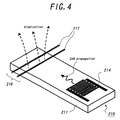
- Fig. 4 is a perspective view depicting an atomizer, including wires as a charging means, in the immobilizing device according to the present invention
- Fig. 1 is a schematic diagram illustrating an exemplary basic configuration of the immobilizing device according to the present invention
- Fig. 2 is an exploded perspective view of an embodiment of the immobilizing device consisting of several components according to the present invention
- Figs. 3A, 3B, and 3C are plain views showing respective surface acoustic wave (SAW) elements, which are used as exemplary components consisting
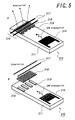
- FIG. 5A is a perspective view representing an atomizer, including both wires as a charging means and a mesh as a particle size controlling means, in the immobilizing device according to the present invention
- Fig. 5B is an exploded perspective view showing components in the atomizer of Fig. 5A
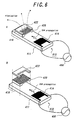
- Fig. 6 is a perspective view illustrating an atomizer, including a monolithic structure body integrated a mesh and spacers, in the immobilizing device according to the present invention
- Fig. 7 is a perspective view showing an atomizer, using a two-dimensional surface acoustic wave element, in the immobilizing device according to the present invention
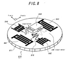
- Fig. 8 is a perspective view of a modification of the atomizer of Fig. 7 Fig.
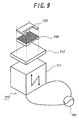
- FIG. 9 is an exploded perspective view depicting an atomizer, including a length vibration mode transducer (or oscillator), in the immobilizing device according to the present invention
- Fig. 10 is an exploded perspective view illustrating an atomizer, including a Peltier element, in the immobilizing device according to the present invention
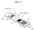
- Fig. 11 is an exploded perspective view representing an atomizer, including reflectors, in the immobilizing device according to the present invention
- Fig. 12 is a cross-sectional view showing an exemplary atomizer in the immobilizing device according to the present invention
- Fig. 13 is a cross-sectional view illustrating a modified atomizer in the immobilizing device according to the present invention
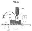
- FIG. 14 is a cross-sectional view depicting an exemplary atomizer without a mesh in the immobilizing device according to the present invention
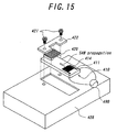
- Fig. 15 is an exploded perspective view representing a supporting arrangement, which supports a SAW substrate and a mesh
- Fig. 16 is a block diagram illustrating a exemplary high frequency (RF) power source used by the immobilizing device according to the present invention
- Fig. 17 is a wave form chart of an exemplary waveform of driving voltage in burst mode, which is supplied to a vibrating element in the immobilizing device according to the present invention
- Fig. 18 is a micrograph obtained by scanning electron microscope (SEM) of a mesh, which is used in the immobilizing device according to the present invention
- Fig. SEM scanning electron microscope
- FIG. 19A is a SEM micrograph at low magnification of a protein (BSA) chip micro structure manufactured by the immobilizing device according to the present invention
- Fig. 19B is a SEM micrograph at high magnification of the protein (BSA) chip micro structure manufactured by the immobilizing device according to the present invention
- Fig. 20A is a proof photograph, obtained under normal illumination, showing degree of activity of a chip manufactured by the immobilizing device according to the present invention
- Fig. 20B is a proof photograph, obtained under dim illumination for easily observing luminescent conditions, illustrating degree of activity of a chip manufactured by the immobilizing device according to the present invention
- Fig. 20A is a proof photograph, obtained under normal illumination, showing degree of activity of a chip manufactured by the immobilizing device according to the present invention
- Fig. 20B is a proof photograph, obtained under dim illumination for easily observing luminescent conditions, illustrating degree of activity of a chip manufactured by the immobilizing device according to the present invention
- FIG. 21 is a photograph depicting degree of activity of a anti-mouse IgG chip manufactured by the immobilizing device according to the present invention
- Figs. 22A and 22B are schematic diagrams, seen on cross section, for showing atomization phenomenon by means of only a vibration
- Figs. 23A and 23B are schematic diagrams, seen on cross section, for depicting atomization phenomenon by means of only an applying electric field
- Fig. 24 is a schematic diagram, seen on cross section, for representing atomization phenomenon by synergistic effect caused by means of both a vibration and an applying electric field
- Fig. 25A is a schematic diagrams, seen on cross section, for schematically showing a principle of a atomizer in the immobilizing device according to the present invention
- Fig. 25B is a schematic perspective view depicting the atomizer of Fig. 25A.
- the immobilizing device comprises precisely controlled solution supply part for feeding a solution such as a Bio macromolecules solution (e.g., a protein), an organic solution, or polymer solution, an atomizer i.e., atomizing part for providing the solution with vibration energy by means of a piezoelectric transducer or a surface acoustic wave (SAW) element or the like, and to atomize the solution into minute particulate substances (or liquid particles), an electrical charging part for electrically charging the solution and the minute particulate substances being atomizing, and a chip forming part for depositing the atomized particulate substances, and to form chips in various patterns in conformity with masks or the like
- a solution such as a Bio macromolecules solution (e.g., a protein), an organic solution, or polymer solution
- an atomizer i.e., atomizing part for providing the solution with vibration energy by means of a piezoelectric transducer or a surface acoustic wave (SAW) element or
- Fig. 1 is a schematic diagram illustrating an exemplary basic configuration of the immobilizing device according to the present invention.
- reference number 10 denotes an atomizer (atomizing part)
- 20 denotes a high voltage power supply
- 30 denotes a collimator electrode(s)
- 40 denotes a fluorocarbon resin shield
- 50 denotes a mask(s)
- 60 denotes sample chip holder
- 70 denotes a chamber (casing)
- 80 denotes precisely controlled solution supply part
- 90 denotes a high frequency power supply.
- the atomizer 10 mainly includes a vibrating element (i.e., substrate) having a flat surface.
- the precisely controlled solution supply part 80 feeds a protein solution onto the flat surface of the substrate in the atomizer 10.
- a predetermined voltage supplied from the high voltage power supply 20 is applied to the solution on the substrate and as a result the solution acquires electrical charges that is the solution is electrically charged.
- electrical charging is accomplished after atomized such that the atomized particulate substances are electrically charged.
- High frequency signal from the high frequency power supply 90 is provided to the substrate in the atomizer 10, due to this signal the substrate (or vibrating element) generates mechanical vibrations therein. Due to the produced vibrations the solution is atomized to be electrically charged particulate substances (i.e., charged fine particles), and to fly out to space in the chamber 70.
- the particulate substances are collected and directed to the sample chip holder 60 by the collimator electrode, the fluorocarbon resin shield 40, and the mask 50, to be deposited (or attached) onto the sample chip holder 60 and as a result the deposited or immobilized chip is formed. It is necessary to keep humidity low or dry condition in the chamber 70, in order to dry the atomized particulate substances.
- a desiccant as a drying means is placed in the chamber 70, instead of the desiccant, the drying means can be various devices such as a circulation unit for supplying a dry air and for recovering it, or a decompression (or vacuum) device. Since the atmosphere in the chamber is kept in low humidity and dry condition due to such devices, the atomized particulate substances can more rapidly be dried to improve the activities of the deposit.
- Fig. 2 is an exploded perspective view of an embodiment of the immobilizing device consisting of several components according to the present invention. That is, the Fig. 2 shows a three dimensional assembly diagram of parts from a part for atomizing to a part for forming a chop, comprised in the immobilizing device according to the present invention, and this allows the clarification of ambiguous illustrations in the two dimensional concept view of Fig. 1 by means of the perspective view or three dimensional assembly diagram.
- the atomizer 10 shown in Fig. 1 can be various kinds of devices. Although several exemplary atomizers will be shown in detail in Figs. 3-11, the embodiment of the exploded perspective view in Fig. 2 uses an atomizer of Fig. 6 by way of example.
- the atomizer 10 consists of a piezoelectric substrate 11 (piezoelectric vibrating element), a monolithic structure 12 (i.e., integrated combination of a mesh and spacers) including a mesh having a plurality of holes separately-placed at certain intervals, a holding plate 13, and an IDT 14 (Inter Digital Transducer) which comprises comb-shaped electrodes.
- a piezoelectric substrate 11 piezoelectric vibrating element
- a monolithic structure 12 i.e., integrated combination of a mesh and spacers
- IDT 14 Inter Digital Transducer
- a surface(s) of the piezoelectric substrate 11, the IDT 14, or the mesh 12 can be subjected to a hydrophilic treatment (or hydrophobic/oleophilic treatment) depending on properties of a solution to be used, wetting properties for solutions can be improved. Thereby it is possible to improve atomizing conditions, that is, to decrease and equalize grain sizes of the particulate substances.
- a hydrophilic (or hydrophobic) film laminated on a surface of them there can be provided.
- a high voltage power supply 20 in Fig. 2 is electrically coupled to a conductor mesh or spacers and carries out a function of providing the solution and/or the atomized particulate substances with electrical charges.
- the power supply capable of supplying 5000 volts of direct current is used, in practice wide range of voltages can be used. Since voltage impacts on a collecting efficiency, properties, or activities of the formed protein chip, it is preferable that the voltage is optimized.
- each collimator electrode 31 has an inside diameter of 80 mm
- the electrode 32 has inside diameter of 75 mm
- the electrode 33 has inside diameter of 70 mm
- the electrode 34 has inside diameter of 65 mm.
- each collimator electrode is gradually reduced as each collimator electrode gets closer to the sample chip holder 60 (i.e., a plate for depositing sample) so that the atomized particulate substances can be collected toward the sample chip holder.
- the high voltage power supply 20 feeds 5000 volts of direct current, as shown in Fig. 2, they are optimized such that, the electrode 31 is 4000 volts, the electrode 32 is 3000 volts, the electrode 33 is 2000 volts, the electrode 34 is 1000 volts, and the electrode 34 is 1000 volts by providing appropriate resistances respectively in a circuit.
- a fluorocarbon resin shield 40 in Fig. 2 acts as a mask to improve a collecting efficiency. Once electrically or electrostatically charged particulate substances (charged protein) are adhered to the fluorocarbon resin shield 40 to form a layer having a certain thickness of the particles, since then newly pieces of charged particulate substances are not adhered to he fluorocarbon resin shield 40 due to electrostatic repelling between the charged deposited layer and the charged flying proteins and thus collecting efficiency is improved. fluorocarbon resin shield 40 in Fig. 2
- surfaces of the sample chip holder 60 in Fig. 2 preferably have electrical conductivity.
- the sample chip holder 60 is preferably made of an ITO glass, an aluminium coated PET (polyethylene terephthalate), a stainless material, or single crystal metal.
- surfaces of the sample chip holder 60 is preferably coated with a PVP, an EDTA, or the like and thus the deposited chip can easily be broken away from the holder.
- Figs. 3A, 3B, and 3C are plain views showing respective surface acoustic wave (SAW) elements, which are used as exemplary components consisting of respective atomizers in the devices according to the present invention.
- Fig. 3A shows a SAW substrate 111 and a surface acoustic wave element 117 having an IDT 114
- Fig. 3B illustrates a surface acoustic wave element 118 further having an reflector 115 at one end thereof
- Fig. 3C depicts a surface acoustic wave element 119 further having reflectors 115 at both ends thereof.
- the piezoelectric material of the surface acoustic wave element is made of 128 degrees rotated y-cut x-propagation LiNbO 3 .
- the IDT 114 is provided on the mirror finished surface of the element, the IDT 114 comprises 20 pairs of pieces, which is 100 ⁇ m in line width and is 400 ⁇ m spacing pitch. Since propagation speed of the Rayleigh wave on the LiNbO 3 is 3960 m/s and the pitch of the electrodes is 400 ⁇ m, wavelength, which can be determined the electrode pitch, should be 9.6 MHz. Although in this embodiment driving frequency is 9.6 MHz and burst cycle is 1Hz, and duty ratio is 1 percent, it is possible to atomize in a condition other than those conditions.
- Fig. 4 is a perspective view depicting an atomizer, including wires as a charging means (or as a part consisting a set of atomizing, charging and vibrating), in the immobilizing device according to the present invention.
- an atomizer 210 comprises a SAW substrate 211, an IDT 214 placed on a surface of the IDT 214, and wires 217. Since the solution is mainly atomized and fried out from the left side of the surface of the substrate 211, this area is referred as atomizing region 216 herein.
- the wires 217 which are connected to a high voltage power supply, is disposed in contact with or above i.e., in the vicinity of the atomizing area 217.
- the wires 217 and the surface of the substrate 211 it is preferable to leave a space between the wires 217 and the surface of the substrate 211, that is, without contacting with the surface thereof, even if the spacing is very short in length. Vibration of the substrate 211 may be attenuated due to the contact. Due to that a predetermined voltage is provided to the wires 217, the protein solution and/or atomized minute particulate substances on the atomizing region 216 are electrically charged to generate charged particulate substances. Alternatively, by providing vibration and charging simultaneously, the solution is atomized into minute particulate substances.
- Fig. 5A is a perspective view representing an atomizer, including both wires as a charging means (or as a part consisting a set of atomizing, charging and vibrating) and a mesh as a particle size controlling means, in the immobilizing device according to the present invention
- Fig. 5B is an exploded perspective view showing components in the atomizer of Fig. 5A.
- an atomizer 310 comprises a piezoelectric SAW substrate, an IDT 314 placed on a surface of the substrate 311, wires 317, a mesh 318, and spacers 319.
- the mesh 318 as a particle size controlling means is disposed between a atomizing region 316 of the substrate 311 and wires 317. Thereby, particle size of the atomized particulate substances can be held to a constant. Particle size of the atomized particulate substances is determined by a hole size of the mesh 318. Although in this embodiment the mesh having holes with a diameter of 10 ⁇ m is used, it can be modified depending on a desired particle size.
- Spacers 319 in this embodiment aluminium foils are used as the spacers) are disposed between the atomizing region 316 of the substrate 311 and the mesh 318. Thereby, a gap between the mesh 318 and the substrate 311 can be kept to a constant.
- Fig. 6 is a perspective view illustrating an atomizer, including a monolithic structure body integrated a mesh and spacers, in the immobilizing device according to the present invention.
- an atomizer 410 comprises a piezoelectric SAW substrate 411, a IDT 414 provided on a surface of the substrate 411, and a monolithic structure body 420, disposed at the atomizing region 416 on the surface of substrate 411, capable of both a mesh and a spacer.
- the IDT 414 is connected to a high voltage power supply 490 and a predetermined high frequency signal for driving is provided to the IDT 414.
- the monolithic structure body 420 is a component integrated combination of a mesh and spacers, and is manufactured such that, after a block is made by both exposure of SU-8 and plating technology and surface roughness and gap of the block is adjusted by ultra-fine machinery processing.
- the monolithic structure body 420 is made of a conductive material and is connected to a high voltage power supply (not shown). Namely the monolithic structure body 420 acts as a charging means, when the solution or the atomized particulate substances make contact with this structure body or pass through the mesh of the structure body, they are electrically charged. Therefore, in this embodiment wires as described above is not needed. Furthermore, there is provided a holding plate 422 on the monolithic structure body 420.
- Fig. 7 is a perspective view showing an atomizer, using a two-dimensional surface acoustic wave element, in the immobilizing device according to the present invention.
- an atomizer 510 (SAW element) comprises a SAW substrate 511, four IDTs 541, 54 2,543, and 544 on the substrate 511, as such an atomizing region 516 located at the center of the SAW substrate 511 is surrounded by these IDTs,
- a pairs of the IDTs 541 and 543 which are facing each other, generates surface acoustic waves (SAWs), which propagates along the direction of x-axis connecting the IDT 541 to the IDT 543, and these SAWs mainly serves to flat (or spread out) the solution layer.
- SAWs surface acoustic waves
- the solution layer gets thinner and thus the atomizing efficiency can be improved or the particle size of the atomized particulate substances may be decreased.
- a remaining pair of the IDTs 542 and 544, which are facing each other, is mainly used for atomizing.
- Discrete high frequency signals are separately provided to the respective IDTs, frequency or voltage of the respective signals can separately be set to desired values for any purposes.
- a deposited metal film 521 on an atomizing region 516 the film 521 is coupled to the high voltage power supply 520, and a predetermined voltage is applied to the film, and the solution (or atomized particulate substances in the vicinity of the deposited metal film) is electrically charged.
- Fig. 8 is a perspective view of a modification of the atomizer of Fig. 7.
- an atomizer 610 comprises a SAW substrate 611 and four IDTs 641, 642, 643, and 644, on the element 611, as such an atomizing region 616 located at the center of the SAW substrate 611 is surrounded by these IDTs.
- a slider 650 is provided on the atomizing region 616 to form a SAW linear motor.
- the SAW linear motor Due to that a high frequency signal is supplied to the IDT 641 (or IDT 643), the SAW linear motor generates SAWs propagating along with X-axis and thus the slider 650 moves along with X-axis by friction force of the SAWs and the slider 650.
- the signal is supplied to the remaining IDT 643 (or 641), SAW direction is inverted and thus the slider moves to the reverse direction. Due to this back-and-forth motion, the solution is flatted and the solution layer gets thinner, and as a result the atomizing efficiency can be improved, or the particle size of the atomized particulate substances may be decreased.
- the slider 650 is preferably pressed with proper strength in a direction toward the substrate.
- Fig. 9 is an exploded perspective view depicting an atomizer, including a length vibration mode transducer (or oscillator), in the immobilizing device according to the present invention.
- an atomizer 710 comprises a piezoelectric substrate 711, a plate 712 disposed on a surface of the substrate 711, and a monolithic structure body 720 serving as both a mesh and s spacer, which is provided on a surface of the plate 712.
- the piezoelectric substrate 711 is connected to a high voltage power supply 791, when a predetermined electric signal is provided to the substrate 711, mechanical vibration, that is, up-and-down movement is generated by the signal. Due to that the generated up-and-down motion is transferred to the solution on the plate 712 through the plate 712, this arrangement is configured such that the atomized fine particles are fly out from the holes of the mesh.
- Fig. 10 is an exploded perspective view illustrating an atomizer, including a Peltier element, in the immobilizing device according to the present invention.
- the Peltier element 425 is placed at the bottom of the SAW substrate 411 in the atomizer 410 shown in Fig. 6B, and a heat sink 426 is placed at the bottom of this Peltier element 425
- the temperature must be controlled.
- the Peltier element 425 can be mounted to the all atomizers described above, if this element 425 is mounted on, since the Peltier element 425 acts as both a cooler and heater, it is possible to more precisely control the temperature.
- Fig. 11 is an exploded perspective view representing an atomizer, including reflectors, in the immobilizing device according to the present invention.
- a reflector(s) 415 is placed on the surface of the SAW substrate 411 in the atomizer 410 shown in Fig. 6B.
- the reflector 415 is provided in this way, surface acoustic waves can efficiently be transmitted to the atomizing region 416, thereby intensity of the vibration may be increased. Therefore, in the last result, it is possible to atomize with a lower voltage and to improve the atomizing efficiency of the solution. Additionally, this reflector can be used for the all atomizers having a SAW element described above.
- Fig. 12 is a cross-sectional view showing an exemplary atomizer in the immobilizing device according to the present invention.
- an atomizer 810 comprises a SAW substrate 811, an IDT 814 placed on a surface of the substrate 811, and a container 822 disposed above the substrate 811, which is integrated combination of a mesh and a tube.
- a solution containing s predetermined sample(s) is supplied to a gap between the substrate 811 and the container 822 through the tube from a pump (not shown) as a liquid supply means.
- the supplied solution on the substrate 811 is conveyed to the right side of the substrate, that is, to an atomizing region 816 by a SAW stream propagating from the left to the right on s surface of the substrate.
- the conveyed solution is atomized in the atomizing region 816 (i.e., beneath the mesh), and the atomized particulate substances are fry out to upward through the mesh.
- the mesh is connected to a high voltage power supply 820, and the solution or the atomized particulate substances is electrically charged while passing through the mesh.
- the flow rate of the solution can be controlled to a desired level by adjusting the pump.
- the flow rate of the solution can be controlled to a desired level by adjusting a intensive of the stream (i.e., controlling a driving voltage).
- Fig. 13 is a cross-sectional view illustrating a modified atomizer in the immobilizing device according to the present invention.
- an atomizer 911 comprises a SAW substrate 911, IDT 914 placed on a surface of the substrate 911, and a container 924 disposed above the substrate 911, which is integrated with a mesh.
- a solution is fed to the container 924 at a proper flow rate in a using an automatic sampler 926.
- the mesh is also connected a high voltage power supply 920, and the solution or the atomized particulate substances is electrically charged while passing through the mesh.
- Fig. 14 is a cross-sectional view depicting an exemplary atomizer without a mesh in the immobilizing device according to the present invention.
- an atomizer 1010 comprises a SAW substrate 1011, an IDT 1014 placed on a surface of the substrate 1011, and a container 1025 disposed above the substrate 1011.
- a solution is fed to the container 1025 from an automatic sampler 1025.
- a predetermined voltage from a high voltage power supply 1020 is applied to the solution via a conductive wire and the solution is electrically charged.
- vibration caused by SAW propagation may easily atomize the solution in an atomizing region 1016 or in the vicinity thereof
- Fig. 15 is an exploded perspective view representing a supporting arrangement, which supports a SAW substrate and a mesh.
- the atomizer 410 shown in Fig. 6A is mounted on a base plate 428. Due to that a holding plate 422 at the top of the atomizer 410 is fixed to the base plate 428 by screws 427, the atomizer 410 is fixed to the base plate 428.
- the atomizer is mechanically fixed and supported like this embodiment.
- various supporting techniques other than that used in this embodiment can be applicable to this device.
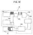
- Fig. 16 is a block diagram illustrating a exemplary high frequency (RF) power source used by the immobilizing device according to the present invention.
- a high frequency power source 90 comprises an oscillator for main frequency 1091, an oscillator for intermittent driving 1092, an AND circuit 1093, a preamplifier 1094, a main amplifier 1095, and an impedance matching circuit 1096.
- An AND operation is performed on a signal from the oscillator for main frequency 1091 and a signal from the oscillator for intermittent driving 1092 in a predetermined duty ratio, to generate a high frequency signal , and the high frequency signal is supplied to an atomizer 10 through the preamplifier 1094, the main amplifier 1095, and the impedance matching circuit 1096.
- the supplied high frequency signal drives the SAW substrate to generate vibrations.
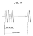
- Fig. 17 is a wave form chart of an exemplary waveform of driving voltage in burst mode, which is supplied to a vibrating element in the immobilizing device according to the present invention.
- the oscillator for intermittent driving 1092 generates a driving voltage signal for burst mode in a desired duty ratio.
- the duty ratio is preferably set to approximately 5-10 percent. Therefore, when the SAW substrate is driven intermittently, due to that an appropriate vibration is generated while temperature rise of the SAW substrate is prevented, the solution can be atomized.
- Fig. 18 is a micrograph obtained by scanning electron microscope (SEM) of a mesh, which is used in the immobilizing device according to the present invention.
- a mesh is processed by a micro machining and inside diameter of the holes in the mesh is 10 ⁇ m.
- This mesh acts as a particle size regulation means.
- the mesh of 10 ⁇ m is used, various kinds of meshes can be used depending on a desired particle size.
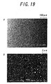
- Fig. 19A is a scanning electron microscope (SEM) micrograph at low magnification of a protein (BSA) chip micro structure manufactured by the immobilizing device according to the present invention
- Fig. 19B is a SEM micrograph at high magnification of the protein (BSA) chip micro structure manufactured by the immobilizing device according to the present invention.
- particle size is 0.2 ⁇ m to 1 ⁇ m as shown in Figs. 19A and 19B
- a chip composed of particles having a desired particle size can be manufactured by changing a vibration condition (i.e., driving voltage) of the atomizer.
- Fig. 20A is a proof photograph, obtained under normal illumination, showing degree of activity of a chip manufactured by the immobilizing device according to the present invention
- Fig. 20B is a proof photograph, obtained under no illumination for easily observing luminescent conditions, illustrating degree of activity of a chip manufactured by the immobilizing device according to the present invention.
- 40 ⁇ l of a luciferase solution (0.25 ⁇ g/ ⁇ l) was atomized to be immobilized as a chip, and then the immobilized chip is dissolved in a reaction solution (luciferin solution) and luminescence status of the solution was observed.
- a reaction solution luciferin solution
- a target tube containing the solution dissolved the chip, which is manufactured by the immobilizing device according to the present invention is located at the upper left part of the image.
- a tube located at the upper right part of the image contains only a reaction solution (luciferin solution)
- a tube located at the lower part of the image contains the solution dissolved the chip, which is manufactured by the immobilizing device according to the present invention, after one hour goes by after dissolved.
- the luciferase (luminescent enzyme) reacted the liciferin (luminescent substrate) and as a result bioluminescence was generated, and this bioluminescence was observed. Namely, it has been found that functional activities of the luciferase can be retained due to the process according to the present invention. Additionally, it has been found that the tube for reference located at upper right part of the image was entirely non-luminescent. Furthermore, the tube located at lower part contained the solution, in which after one hour went by after the solution for the upper left tube was made, in this circumstance it has been found that there existed weak bioluminescence.
- luciferase used in this embodiment has a very low stability, if once the buffering agent is excluded, this substance instantly loses its activities, it is impossible to manufacture a chip of this substance using a conventional ESD method.
- the immobilizing device of the present invention even if such a substance having a lower stability, since such a substance tin the presence of the buffering agent can be atomized and immobilized, this device has a great advantage.
- Fig. 21 is a photograph depicting degree of activity of a anti-mouse IgG chip manufactured by the immobilizing device according to the present invention. Namely, this photograph is an image for evaluating a fluorescence intensity of anti-mouse IgG contained in the chip, which is manufactured such that anti-mouse IgG is atomized, cross-linked, and immobilized, to form a chip, and to react it. As shown in Fig. 21, it could be observed that there was emission of light by fluorescence (in the image, this area can be observed as white) over all of the chip. In this way, due to use of this immobilizing device, an anti-mouse IgG chip retaining its activities can be formed.
- Figs. 22A and 22B are schematic diagrams, seen on cross section, for showing atomization phenomenon by means of only a vibration.
- Fig. 22A shows schematic diagram where weak vibration is excited, as shown in Fig. 22A, in a condition that there is liquid on a substrate 1200 such as a piezoelectric element or the like, when weak vibration is excited on the substrate 1200, the weak vibration is transmitted to the liquid, and thus small waves are generated on the liquid surface.
- a substrate 1200 such as a piezoelectric element or the like
- Fig. 22B shows schematic diagram where strong vibration is excited, as shown in Fig. 22B when there is provided sufficiently strong vibration, very big waves are generated on the liquid surface. At this time if movement velocity in the vicinity of the liquid surface is sufficiently high, a piece of the liquid is flied out as droplets while throwing off a binding force by a surface tension.
- vibration is expressed as surface acoustic waves (SAW), even if the vibration is in different vibration modes such as a travelling-wave, a bending wave, an axial vibration, or a lateral vibration, it can be conceived that the same interpretation is satisfied.
- SAW surface acoustic waves
- FIGs. 23A and 23B are schematic diagrams, seen on cross section, for depicting atomization phenomenon by means of only an applying electric field.
- Fig. 23A shows schematic diagram where weak electrical field is applied, as shown in Fig. 23A, in a condition that there is liquid on a substrate 1300 such as a piezoelectric element or the like, when weak electric field (or voltage) is applied to the substrate 1300, in this circumstance the liquid surface is electrically charged, since the liquid surface is not completely isotropic, a part, win which collects the electric charges, is locally generated.
- intensity of the electrical field is not efficiently high (that is weak electrical field)
- the liquid can not be atomized.
- FIG. 23B shows schematic diagram where strong electrical field is applied, as shown in Fig. 23B, in a condition that there is liquid on a substrate 1300 such as a piezoelectric element or the like, when sufficiently strong electric field (or voltage) is applied to the substrate 1300, a piece of the liquid is flied out as droplets toward the air (in direction of the electrical field) while throwing off a binding force by a surface tension due to electrostatic force, in which the electrical charges are subjected by the electrical field.
- a substrate 1300 such as a piezoelectric element or the like
- the substrate is made of a conductive material or there is provided electrodes in the liquid, or there is provided other electrodes at upper part of the Figs or the like for generating electrical field, these components are not shown.
- Fig. 24 is a schematic diagram, seen on cross section, for representing atomization phenomenon by synergistic effect caused by means of both a vibration and an applying electric field.
- electrical field is applied during providing vibration to a substrate 1400, it gives rise to the phenomenon of focusing the electrical charges on the vicinity of the crests of the wave 1420 caused by the vibration. This phenomenon is caused by a physical lay that electrical charges focus on a point having a small value of curvature radius.
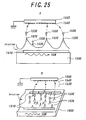
- Fig. 25A is a schematic diagrams, seen on cross section, for schematically showing a principle of a atomizer in the immobilizing device according to the present invention
- Fig. 25B is a schematic perspective view depicting the atomizer of Fig. 25A.
- these drawings are schematic diagram illustrating the immobilizing device using the atomization phenomenon of combined effect caused by both "vibration" and "applying electrical field”.
- an atomizer comprises a vibrating element 1500, and wires 1510 as a charging means disposed on the element.
- a predetermined driving voltage is supplied to the vibration element to generate a surface acoustic wave(s) (SAWs).
- SAWs surface acoustic wave(s)
- the solution When a protein solution is supplied onto the vibrating element, the solution receives the SAW from the vibrating element, waves as shown are generated, and to form an endless number of crests 1520 of wave in succession. In other words, a great number of prongs like a tip of a capillary are formed on the solution surface.
- the wires 1510 are connected to a high voltage power source (not shown), and a high voltage is applied to the solution.
- the electrical charges generated by this applying will focus on crests (prongs) of wave 1520, which are generated by the vibration, of the solution.
- a piece of the solution, on which the electrical charges focus on, will electrostatically jump out of the crests 1520 upward as charged minute particulate substances 1530.
- a solvent(s) or water is dried off and thus the particles will decrease its particle size. Additionally, it may happen that the particulate substances 1530 split into pieces by electrical repulsive force within each particles 1530.
- the particulate substances 1530 are immobilized on the substrate 1550 for immobilizing sample, which faces the vibrating element 1500 for immobilizing sample, in a dry form as spots 1540.
- the present invention is a technique for ruffling the solution on the vibrating element substrate by vibrating, to form an endless number of the prong pats, and the same time for focusing electrical charges on the prong parts by applying a high voltage, and thereby the solution can be electstatically be atomized as electstatically charged minute particulate substances.
- the immobilizing device of the present invention since a sample solution is atomized by simultaneously applying mechanical vibration and charging, even if a solution in higher conductivity, that is, a solution without excluding the buffer agent is used, such a solution can be atomized, and as a result it is possible that a sample can be immobilized in a status retaining more highly activities thereof.
- the present device can be used as a deposition device, or a microarray (DNA chip) manufacturing device. Since the immobilizing device of the present invention uses no capillary, the present invention has the remarkable advantage that it is low cost and it is easy to maintain, because processing speed and atomizing efficiency can easily be increased by just extending an area or size of the vibrating element in this device.
Landscapes
- Health & Medical Sciences (AREA)
- Chemical & Material Sciences (AREA)
- Immunology (AREA)
- Life Sciences & Earth Sciences (AREA)
- Engineering & Computer Science (AREA)
- Urology & Nephrology (AREA)
- Biomedical Technology (AREA)
- Organic Chemistry (AREA)
- Hematology (AREA)
- Molecular Biology (AREA)
- Biochemistry (AREA)
- Chemical Kinetics & Catalysis (AREA)
- Food Science & Technology (AREA)
- Medicinal Chemistry (AREA)
- Physics & Mathematics (AREA)
- Analytical Chemistry (AREA)
- Cell Biology (AREA)
- General Health & Medical Sciences (AREA)
- General Physics & Mathematics (AREA)
- Pathology (AREA)
- Biotechnology (AREA)
- Microbiology (AREA)
- Electrostatic Spraying Apparatus (AREA)
- Sampling And Sample Adjustment (AREA)
- Special Spraying Apparatus (AREA)
- Apparatuses For Generation Of Mechanical Vibrations (AREA)
- Measuring Or Testing Involving Enzymes Or Micro-Organisms (AREA)
- Supplying Of Containers To The Packaging Station (AREA)
- Seal Device For Vehicle (AREA)
- Container Filling Or Packaging Operations (AREA)
- Investigating Or Analysing Biological Materials (AREA)
- Physical Or Chemical Processes And Apparatus (AREA)
Abstract
Description
Although there has been developed and practically used various devices and techniques for forming such films or thin layers, such conventional devices and methods have not always been applicable to immobilize or deposit biomolecules or of functional macromolecules and to form such films in which activities and functionalities of them are kept due to following reasons.
For example, there are conventional sputtering devices, Electron Beam (EB) resistance heating type vapor deposition sputtering devices, and chemical vapor deposition apparatuses, and they are practically used for forming films of metals or inorganic compounds. However, since in such devices a substance contained in the films must be exposed to plasma or high temperature under high vacuum, if the substance to be processed is biological macromolecules or organic macromolecules it is almost impossible to immobilize or deposit the substance to form a film or a thin layer in which the activities and functionalities of that are kept.
In addition, in case of bio macromolecules or the like which must be dissolved in a buffering solution, or an organic polymers, which have high electrical conductivities, since they have high conductivity, they cannot be processed even by the ESD method and thus it is impossible to form a film of them.
Namely, in any conventional methods or devices it is impossible to form a film of bio macromolecules or functional polymers, in the form of a desired shape or thickness without loosing biological activities or functionalities of that, from small amount of substances.
Although the conventional ESD method cannot use a sample solution having high electrical conductivity (in case of solution containing a buffering agent having a high electrical conductivity), since the present immobilizing device according to the present invention atomizes the solution utilizing mechanical vibration and electrical charging at the same time, the present immobilizing device can use a sample solution having high electrical conductivity. Namely, because, when a protein is immobilized or deposited, the present device has no occasion to remove a buffering agent, which acts to retain proteins in a stable state, from the sample solution, the present device has the advantage that there is no need to complete a series of operations regarding forming a film or thin layer in a shot time of period. Additionally the present device can produce a thin layer or a film including a sample(s) having higher activities. In addition, although the conventional ESD method needs a solution containing completely dissolved samples so as to avoid choke up with the non-dissolved samples in an opening of capillary tip, the present device can use a sample having low solubility in a form that the pieces of sample are dispersed in a solution and therefore has a very practical use.
the device further comprises a collecting means for collecting said atomized and charged minute particulate substances by electrostatic forces, and to direct said substances onto said substrate.
According to this arrangement, since the atomized minute particulate substances can efficiently be collected and directed to the substrate, efficiency of the immobilizing is increased.
the device further comprises a means for regulating temperature of at least one of said vibrating element, said substrate, and said solution or solvent.
Alternatively, in a modified embodiment, the device further comprises:
said charging means comprises at least one of a conductive wire, a conductive membrane, a conductive mesh, and a device for emitting charged ions.
According to this arrangement, the solution, the atomized particulate substances, or the particulate substances being atomized can efficiently be electrostatically charged.
the device further comprises a liquid supplying means for feeding said solution (or solvent) onto said vibrating element in a predetermined rate of flow.
According to this arrangement, the solution (or solvent) is fed onto the surface of the vibrating element at an appropriate flow rate by a pump or the like, so that the immobilized sample can be manufactured in proportion as a desired atomizing process speed.
at least a part of a surface of said vibrating element opposed to said substrate is subjected to a hydrophilic or hydrophobic treatment.
According to this arrangement, the vibrating element is subjected to hydrophilic (or hydrophobic treatment) in response to properties of the solution (or solvent) to be used, or the vibrating element (or its surface) can be made of a hydrophilic material, sot that wetting property for the solution can be improved. Therefore, conditions of atomizing the solution can be improved, that is the particulate substances can be split into minute pieces or particle sizes can be equalized.
said vibrating element comprises a spreading means for spreading out said solution (or solvent) as a thin layer on said vibrating element.
Conditions or efficiency of the atomizing the solution are improved when the thickness of solution layer on the vibrato surface is decreased. Therefore according to this arrangement, since said solution (or solvent) is spread out as a thin layer on said vibrating element, Conditions or efficiency of the atomizing the solution are improved. In addition, in proportion to the solution layer on the vibrating element is reduced , the solution can be atomized with lower frequency of vibration and thus electricity can be saved.
the devices further comprises a particle size control means disposed between the vibrating element and the substrate for controlling sizes of said particulate substances.
Sizes of the particulate substances have much effect on properties of films or spots manufactured. In particular, when the droplets sizes are too large, solvent included in the solution is not completely evaporated till the atomized pieces of the solution are arrived at the substrate and thus activities of the sample are degraded. As just described, although ,in many case, samples can stably retain its activities either in a buffer solution or in a dry form, activities of the sample in middle of the drying process will rapidly be decreased. According to this arrangement, in order to rapidly and completely evaporate the sample solution till the sample solution arrives on the substrate, the sizes of the particulate substances can be regulated to desired sizes small enough and to avoid the activities of the sample from degrading. Specifically, the particle size control means can be a mesh having minute holes.
said collecting means comprises one or more convergence electrodes disposed between the vibrating element and the substrate.
According to this arrangement, by applying voltage, which has the same pole as the electric charges on the particulate substances, to the convergence electrodes, the convergence electrodes repel the charged particulate substances electrostatically and thus the charged particulate substances are efficiently directed to the substrate and to improve collecting efficiency of the particulate substances.
said collecting means comprises one or more masks which are made of an insulating or dielectric material and disposed between the vibrating element and the substrate.
According to this arrangement, desired pattern films can be manufactured depending on shapes of the masks. In addition, when an insulating or dielectric material is used as the mask, once the charged particulate substances are attached on the masks to form a layer having a certain thickness, since then newly pieces of charged particulate substances are not attached due to electrostatic repelling and thus collecting efficiency is improved.
the devices further comprises a drying means for drying said particulate substances and wherein said drying means comprises at least one of means for supplying dry air, means for reducing pressure, and means for forming a vacuum.
According to this arrangement, the atomized particulate substances can rapidly be dried and thus the films or spots of the sample, in which its activities are highly retained, can be manufactured.
at least a part of a surface, which is faced to the vibrating element, of said substrate is made of a conductive material and is grounded.
Alternatively, in a modified embodiment, said at least a part of the surface made of the conductive material has one or more desired pattern regions.
According to these arrangements, since the grounded conductive material pulls the charged particulate substances, films or the like may efficiently be formed. Additionally, electrical charges of the deposited charged particulate substances are drained away by the grounding.
In addition, when conductive material is placed with a desired pattern (e.g., a spotted pattern) on the substrate surface, in other words, a part of conductive material is exposed on the substrate surface such a pattern, pieces of the particulate substances can be deposited only on the exposed region and thus even if small quantity sample solution is used it may be immobilized.
Additionally, since respective formed spots are separated each other, separate regents can easily be dropped to each of spots and thus there is an advantage that functional properties of the sample for various reagents may be tested simultaneously and quickly.
said vibrating element is activated intermittently on a predetermined cycle.
According to this arrangement, it is possible to avoid the vibrating element from reaching a high temperature. Since it can be prevented that sample solution, which has a weakness for temperature change, is subjected to high temperature, films or the like having activities, which are more highly retained, may be manufactured.
said vibrating element is an ultrasonic transducer, an electrostatic transducer, a piezoelectric transducer, a magneto-striction transducer, an electrostriction transducer, or an electromagnetic transducer.
In yet another embodiment of the immobilizing device according to the present invention,
said piezoelectric transducer is a mono-layer structure transducer, a multiplayer structure transducer, or a single crystal transducer.
In yet another embodiment of the immobilizing device according to the present invention,
said piezoelectric transducer is a resonant transducer, a surface acoustic wave (SAW) transducer, a length vibration mode transducer, a thickness sheer mode transducer, a radial vibration mode transducer, a thickness vibration mode transducer, or a longitudinal vibration mode transducer.
said SAW transducer comprises one or more inter digital transducers (IDTs).
According to this arrangement, since the vibration conditions of the vibrating element can more precisely be controlled due to providing one or more inter digital transducers (IDTs) and as a result the sample solution is minutely atomized, atomization efficiency is increased.
the device further comprises a means for feeding said solution or solvent onto a region, at a distance from said IDTs, of said SAW transducer in a predetermined rate of flow, and to hold said fed solution or solvent on a predetermined region of said SAW transducer.
In IDTs of the SAW transducer, if each electrode consisted of IDTs shorts out another one, elastic waves cannot be generated. In order to prevent this, it is necessary to set apart or separate each electrode from other electrodes in a predetermined pitch. Therefore, it is necessary to avoid a sample having high electrical conductivity from contacting an electrode to short out, Consequently, due to that the solution is fed onto a region at a sufficiently distance from the electrodes (i.e., IDTs) as this arrangement, short circuit of the electrodes can be prevented. In order to hold the solution on a certain region, for example, A mesh as a particle size control means or a wire(s) as a charging means is located on or in the vicinity of the vibrating element. Due to arranging the mesh or wire in this way, it can advantageously be prevented that the solution flows out from the vibrating element or flows back to the electrodes. Additionally, a mesh or the like as a particle size controlling means is preferably located on or over the region holding the solution, because the solution is mainly atomized in the region, in which the solution is held therein.
said SAW transducer comprises one or more reflectors.
According to this arrangement, due to utilizing effectively surface acoustic waves, the solution can finely be atomized to increase atomizing efficiency.
Fig. 2 is an exploded perspective view of an embodiment of the immobilizing device consisting of several components according to the present invention;
Figs. 3A, 3B, and 3C are plain views showing respective surface acoustic wave (SAW) elements, which are used as exemplary components consisting of respective atomizers in the devices according to the present invention;
Fig. 4 is a perspective view depicting an atomizer, including wires as a charging means, in the immobilizing device according to the present invention;
Fig. 5A is a perspective view representing an atomizer, including both wires as a charging means and a mesh as a particle size controlling means, in the immobilizing device according to the present invention;
Fig. 5B is an exploded perspective view showing components in the atomizer of Fig. 5A;
Fig. 6 is a perspective view illustrating an atomizer, including a monolithic structure body integrated a mesh and spacers, in the immobilizing device according to the present invention;
Fig. 7 is a perspective view showing an atomizer, using a two-dimensional surface acoustic wave element, in the immobilizing device according to the present invention;
Fig. 8 is a perspective view of a modification of the atomizer of Fig. 7
Fig. 9 is an exploded perspective view depicting an atomizer, including a length vibration mode transducer (or oscillator), in the immobilizing device according to the present invention;
Fig. 10 is an exploded perspective view illustrating an atomizer, including a Peltier element, in the immobilizing device according to the present invention;
Fig. 11 is an exploded perspective view representing an atomizer, including reflectors, in the immobilizing device according to the present invention;
Fig. 12 is a cross-sectional view showing an exemplary atomizer in the immobilizing device according to the present invention;
Fig. 13 is a cross-sectional view illustrating a modified atomizer in the immobilizing device according to the present invention;
Fig. 14 is a cross-sectional view depicting an exemplary atomizer without a mesh in the immobilizing device according to the present invention;
Fig. 15 is an exploded perspective view representing a supporting arrangement, which supports a SAW substrate and a mesh;
Fig. 16 is a block diagram illustrating a exemplary high frequency (RF) power source used by the immobilizing device according to the present invention;
Fig. 17 is a wave form chart of an exemplary waveform of driving voltage in burst mode, which is supplied to a vibrating element in the immobilizing device according to the present invention;
Fig. 18 is a micrograph obtained by scanning electron microscope (SEM) of a mesh, which is used in the immobilizing device according to the present invention;
Fig. 19A is a SEM micrograph at low magnification of a protein (BSA) chip micro structure manufactured by the immobilizing device according to the present invention;
Fig. 19B is a SEM micrograph at high magnification of the protein (BSA) chip micro structure manufactured by the immobilizing device according to the present invention;
Fig. 20A is a proof photograph, obtained under normal illumination, showing degree of activity of a chip manufactured by the immobilizing device according to the present invention;
Fig. 20B is a proof photograph, obtained under dim illumination for easily observing luminescent conditions, illustrating degree of activity of a chip manufactured by the immobilizing device according to the present invention;
Fig. 21 is a photograph depicting degree of activity of a anti-mouse IgG chip manufactured by the immobilizing device according to the present invention;
Figs. 22A and 22B are schematic diagrams, seen on cross section, for showing atomization phenomenon by means of only a vibration;
Figs. 23A and 23B are schematic diagrams, seen on cross section, for depicting atomization phenomenon by means of only an applying electric field;
Fig. 24 is a schematic diagram, seen on cross section, for representing atomization phenomenon by synergistic effect caused by means of both a vibration and an applying electric field;
Fig. 25A is a schematic diagrams, seen on cross section, for schematically showing a principle of a atomizer in the immobilizing device according to the present invention; and
Fig. 25B is a schematic perspective view depicting the atomizer of Fig. 25A.
The immobilizing device according to the present invention comprises precisely controlled solution supply part for feeding a solution such as a Bio macromolecules solution (e.g., a protein), an organic solution, or polymer solution, an atomizer i.e., atomizing part for providing the solution with vibration energy by means of a piezoelectric transducer or a surface acoustic wave (SAW) element or the like, and to atomize the solution into minute particulate substances (or liquid particles), an electrical charging part for electrically charging the solution and the minute particulate substances being atomizing, and a chip forming part for depositing the atomized particulate substances, and to form chips in various patterns in conformity with masks or the like
Alternatively, there are provided several grooves (not shown) at the in the
Spacers 319 (in this embodiment aluminium foils are used as the spacers) are disposed between the
A remaining pair of the
Discrete high frequency signals are separately provided to the respective IDTs, frequency or voltage of the respective signals can separately be set to desired values for any purposes.
There is provided a deposited
Furthermore, a
A solution containing s predetermined sample(s) is supplied to a gap between the
According to this arrangement, the flow rate of the solution can be controlled to a desired level by adjusting the pump. Furthermore, the flow rate of the solution can be controlled to a desired level by adjusting a intensive of the stream (i.e., controlling a driving voltage).
An AND operation is performed on a signal from the oscillator for
Using the immobilizing device according to the present invention, 40 µl of a luciferase solution (0.25 µg/µl) was atomized to be immobilized as a chip, and then the immobilized chip is dissolved in a reaction solution (luciferin solution) and luminescence status of the solution was observed. As shown in Fig. 20A, a target tube containing the solution dissolved the chip, which is manufactured by the immobilizing device according to the present invention is located at the upper left part of the image. There are provided other two tubes for comparison, a tube located at the upper right part of the image contains only a reaction solution (luciferin solution), and a tube located at the lower part of the image contains the solution dissolved the chip, which is manufactured by the immobilizing device according to the present invention, after one hour goes by after dissolved.
Additionally, it has been found that the tube for reference located at upper right part of the image was entirely non-luminescent. Furthermore, the tube located at lower part contained the solution, in which after one hour went by after the solution for the upper left tube was made, in this circumstance it has been found that there existed weak bioluminescence. Therefore, it has been found that functional activities of the luciferase can be "highly" retained due to the process according to the present invention.
In addition, luciferase used in this embodiment has a very low stability, if once the buffering agent is excluded, this substance instantly loses its activities, it is impossible to manufacture a chip of this substance using a conventional ESD method. In this way, according to the immobilizing device of the present invention, even if such a substance having a lower stability, since such a substance tin the presence of the buffering agent can be atomized and immobilized, this device has a great advantage.
Fig. 24 is a schematic diagram, seen on cross section, for representing atomization phenomenon by synergistic effect caused by means of both a vibration and an applying electric field. As shown in Fig. 24, if electrical field is applied during providing vibration to a
As described above, due to the combined effect caused by that the technique for providing mechanical vibration by a piezoelectric element or the like to a liquid and a technique for applying electrical field are simultaneously performed, even if it is done under a harder condition, the atomization can efficiently and effectively be performed.
As described above, the present invention is a technique for ruffling the solution on the vibrating element substrate by vibrating, to form an endless number of the prong pats, and the same time for focusing electrical charges on the prong parts by applying a high voltage, and thereby the solution can be electstatically be atomized as electstatically charged minute particulate substances.
In this connection, it may happen that on the vibrating element there occurs an atomization caused by only the vibration, and the same time there occurs an atomization caused by only the applying the electrical field, other than the atomization by the electrostatic force
Since the immobilizing device of the present invention uses no capillary, the present invention has the remarkable advantage that it is low cost and it is easy to maintain, because processing speed and atomizing efficiency can easily be increased by just extending an area or size of the vibrating element in this device.
Claims (36)
- An immobilizing device comprising:a vibrating element for vibrating a solution or a solvent containing at least one sample, to atomize the solution or solvent into minute particulate substances whose activities and functionalities are kept;charging means for electrically charging said solution or solvent and/or said minute particulate substances; andsupporting means for supporting a substrate on which said charged minute particulate substances are deposited by electrostatic forces.
- The immobilizing device according to claim 1, wherein the device further comprises collecting means for collecting said atomized and charged minute particulate substances by electrostatic forces, and to direct said substances onto said substrate.
- The immobilizing device according to claim 2, wherein said collecting means comprises one or more masks which are made of an insulating or dielectric material and disposed between the vibrating element and the substrate and/or one or more convergence electrodes disposed between the vibrating element and the substrate.
- The immobilizing device according to claim 1, wherein the device further comprises means for regulating temperature of at least one of said vibrating element, said substrate, and said solution or solvent.
- The immobilizing device according to claim 1, wherein said charging means comprises at least one of a conductive wire, a conductive membrane, a conductive mesh, and a device for emitting charged ions.
- The immobilizing device according to claim 1, wherein the device further comprises liquid supplying means for feeding said solution or solvent onto said vibrating element in a predetermined rate of flow.
- The immobilizing device according to claim 1, wherein at least a part of a surface of said vibrating element opposed to said substrate is subjected to a hydrophilic or hydrophobic treatment.
- The immobilizing device according to claim 1, wherein said vibrating element comprises spreading means for spreading out said solution or solvent as a thin layer on said vibrating element.
- The immobilizing device according to claim 1, wherein the devices further comprises particle size control means disposed between the vibrating element and the substrate for controlling sizes of said particulate substances.
- The immobilizing device according to claim 1, wherein the devices further comprises drying means for drying said particulate substances and wherein said drying means comprises at least one of means for supplying dry air, means for reducing pressure, and means for forming a vacuum.
- The immobilizing device according to claim 1, wherein at least a part of a surface, which is faced to the vibrating element, of said substrate is made of a conductive material and is grounded.
- The immobilizing device according to claim 11, wherein said at least a part of the surface made of the conductive material has one or more desired pattern regions.
- The immobilizing device according to claim 1, wherein said vibrating element is activated intermittently.
- The immobilizing device according to claim 1, wherein said vibrating element is an ultrasonic transducer, an electrostatic transducer, a piezoelectric transducer, a magneto-striction transducer, an electrostriction transducer, or an electromagnetic transducer.
- The immobilizing device according to claim 14, wherein said piezoelectric transducer is a mono-layer structure transducer, a multiplayer structure transducer, a single crystal transducer, a resonant transducer, a surface acoustic wave (SAW) transducer, a length vibration mode transducer, a thickness sheer mode transducer, a radial vibration mode transducer, a thickness vibration mode transducer, or a longitudinal vibration mode transducer.
- The immobilizing device according to claim 15, wherein said SAW transducer comprises one or more inter digital transducers (IDTs).
- The immobilizing device according to claim 16, wherein the device further comprises means for feeding said solution or solvent onto a region, at a distance from said IDTs, of said SAW transducer in a predetermined rate of flow, and to hold said fed solution or solvent on a predetermined region of said SAW transducer.
- The immobilizing device according to claim 15, wherein said SAW transducer comprises one or more reflectors.
- An immobilizing device comprising:and wherein the device is configured to atomize the solution or solvent into minute particulate substances whose activities and functionalities are kept, by vibrations of said solution or solvent with said vibrating element and by electrostatic forces of said charged solution or solvent with said charging means,a vibrating element for vibrating a solution or a solvent containing at least one sample; andcharging means disposed on said vibrating element for electrically charging said solution or solvent,
and wherein said device further comprises supporting means for supporting a substrate on which said charged minute particulate substances are deposited by electrostatic forces. - The immobilizing device according to claim 19, wherein the device further comprises collecting means for collecting said atomized and charged minute particulate substances by electrostatic forces, and to direct said substances onto said substrate.
- The immobilizing device according to claim 20, wherein said collecting means comprises one or more masks which are made of an insulating or dielectric material and disposed between the vibrating element and the substrate and/or one or more convergence electrodes disposed between the vibrating element and the substrate.
- The immobilizing device according to claim 19, wherein the device further comprises means for regulating temperature of at least one of said vibrating element, said substrate, and said solution or solvent.
- The immobilizing device according to claim 19, wherein said charging means comprises at least one of a conductive wire, a conductive membrane, a conductive mesh, and a device for emitting charged ions.
- The immobilizing device according to claim 19, wherein the device further comprises liquid supplying means for feeding said solution or solvent onto said vibrating element in a predetermined rate of flow.
- The immobilizing device according to claim 19, wherein at least a part of a surface of said vibrating element opposed to said substrate is subjected to a hydrophilic or hydrophobic treatment.
- The immobilizing device according to claim 19, wherein said vibrating element comprises spreading means for spreading out said solution or solvent as a thin layer on the vibrating element.
- The immobilizing device according to claim 19, wherein the devices further comprises particle size control means disposed between the vibrating element and the substrate for controlling sizes of said particulate substances.
- The immobilizing device according to claim 19, wherein the devices further comprises drying means for drying said particulate substances and wherein said drying means comprises at least one of means for supplying dry air, means for reducing pressure, and means for forming a vacuum.
- The immobilizing device according to claim 19, wherein at least a part of a surface of said substrate is made of a conductive material and is grounded.
- The immobilizing device according to claim 29, wherein said at least a part of the surface made of the conductive material has one or more desired pattern regions.
- The immobilizing device according to claim 19, wherein said vibrating element is activated intermittently.
- The immobilizing device according to claim 19, wherein said vibrating element is an ultrasonic transducer, an electrostatic transducer, a piezoelectric transducer, a magneto-striction transducer, an electrostriction transducer, or an electromagnetic transducer.
- The immobilizing device according to claim 32, wherein said piezoelectric transducer is a mono-layer structure transducer, a multiplayer structure transducer, a single crystal transducer, a resonant transducer, a surface acoustic wave (SAW) transducer, a length vibration mode transducer, a thickness sheer mode transducer, a radial vibration mode transducer, a thickness vibration mode transducer, or a longitudinal vibration mode transducer.
- The immobilizing device according to claim 33, wherein said SAW transducer comprises one or more inter digital transducers (IDTs).
- The immobilizing device according to claim 34, wherein the device further comprises means for feeding said solution or solvent onto a region, at a distance from said IDTs, of said SAW transducer in a predetermined rate of flow, and to hold said fed solution or solvent on a predetermined region of said SAW transducer.
- The immobilizing device according to claim 33, wherein said SAW transducer comprises one or more reflectors.
Applications Claiming Priority (3)
| Application Number | Priority Date | Filing Date | Title |
|---|---|---|---|
| JP2001339593A JP4025055B2 (en) | 2001-11-05 | 2001-11-05 | Immobilization device |
| JP2001339593 | 2001-11-05 | ||
| PCT/JP2002/011530 WO2003039759A1 (en) | 2001-11-05 | 2002-11-05 | Immobilizing device |
Publications (3)
| Publication Number | Publication Date |
|---|---|
| EP1452239A1 true EP1452239A1 (en) | 2004-09-01 |
| EP1452239A4 EP1452239A4 (en) | 2007-03-14 |
| EP1452239B1 EP1452239B1 (en) | 2009-03-11 |
Family
ID=19153920
Family Applications (1)
| Application Number | Title | Priority Date | Filing Date |
|---|---|---|---|
| EP02779996A Expired - Lifetime EP1452239B1 (en) | 2001-11-05 | 2002-11-05 | Immobilizing device |
Country Status (7)
| Country | Link |
|---|---|
| US (1) | US7516714B2 (en) |
| EP (1) | EP1452239B1 (en) |
| JP (1) | JP4025055B2 (en) |
| AT (1) | ATE424935T1 (en) |
| AU (1) | AU2002344455B2 (en) |
| DE (1) | DE60231540D1 (en) |
| WO (1) | WO2003039759A1 (en) |
Cited By (4)
| Publication number | Priority date | Publication date | Assignee | Title |
|---|---|---|---|---|
| WO2006096303A3 (en) * | 2005-03-04 | 2006-11-09 | Boston Scient Scimed Inc | Production of powder particles utilizing a vibrating mesh nebulizer for coating a medical appliance |
| WO2007070957A1 (en) * | 2005-12-21 | 2007-06-28 | Monash University | Process and apparatus for generating particles |
| WO2009145099A1 (en) * | 2008-05-27 | 2009-12-03 | Panasonic Electric Works Co., Ltd. | Atomization apparatus |
| EP3954414A4 (en) * | 2019-04-09 | 2023-03-22 | Japan Tobacco Inc. | AEROSOL SUPPLY DEVICE |
Families Citing this family (37)
| Publication number | Priority date | Publication date | Assignee | Title |
|---|---|---|---|---|
| DE10327430A1 (en) * | 2003-06-18 | 2005-01-05 | Abb Patent Gmbh | Ultrasonic standing-wave atomizer |
| JP4247554B2 (en) * | 2003-07-30 | 2009-04-02 | 独立行政法人理化学研究所 | Mechanochemical sensor |
| JP4507239B2 (en) * | 2003-09-16 | 2010-07-21 | 祥子 塩川 | Heating device using surface acoustic waves |
| JP4925242B2 (en) * | 2005-04-25 | 2012-04-25 | パナソニック株式会社 | Deodorizer |
| JP5207334B2 (en) * | 2006-02-28 | 2013-06-12 | 独立行政法人理化学研究所 | Micropattern forming apparatus, micropattern structure, and manufacturing method thereof |
| JP4709059B2 (en) * | 2006-04-28 | 2011-06-22 | キヤノン株式会社 | Inspection apparatus and inspection method |
| JP2008049230A (en) * | 2006-08-22 | 2008-03-06 | Tamura Seisakusho Co Ltd | Atomizer |
| JP2008073570A (en) * | 2006-09-19 | 2008-04-03 | Seiko Epson Corp | Atomizer, suction device |
| JP4915567B2 (en) * | 2006-10-26 | 2012-04-11 | パナソニック株式会社 | Surface acoustic wave atomizer |
| JP4961607B2 (en) * | 2006-11-24 | 2012-06-27 | 本多電子株式会社 | Ultrasonic atomizer |
| KR101382738B1 (en) * | 2007-01-10 | 2014-04-08 | 엘지전자 주식회사 | Apparatus and method for forming pattern by electrostactic spray, and method for manufacturing display panel |
| JP4880540B2 (en) * | 2007-08-03 | 2012-02-22 | パナソニック株式会社 | Sample deposition equipment |
| JP5080178B2 (en) * | 2007-09-03 | 2012-11-21 | 日本電波工業株式会社 | Resist coating device |
| JP5080177B2 (en) * | 2007-09-03 | 2012-11-21 | 日本電波工業株式会社 | Resist coating device |
| JP5491189B2 (en) | 2007-11-07 | 2014-05-14 | 明彦 谷岡 | Immobilization device |
| CN102196866B (en) * | 2008-10-24 | 2014-08-06 | 松下电器产业株式会社 | Surface acoustic wave atomizer |
| JP5238453B2 (en) * | 2008-10-27 | 2013-07-17 | パナソニック株式会社 | Electrostatic atomizer |
| JP5347683B2 (en) * | 2009-04-22 | 2013-11-20 | パナソニック株式会社 | Surface acoustic wave atomizer |
| JP2010269278A (en) * | 2009-05-25 | 2010-12-02 | Panasonic Electric Works Co Ltd | Surface acoustic wave atomizer |
| JP2011011102A (en) * | 2009-06-30 | 2011-01-20 | Panasonic Electric Works Co Ltd | Surface acoustic wave atomizer |
| JP5518437B2 (en) * | 2009-11-11 | 2014-06-11 | パナソニック株式会社 | Surface acoustic wave atomizer |
| KR20130095941A (en) * | 2012-02-21 | 2013-08-29 | 건국대학교 산학협력단 | Apparatus for large area deposition using surface acoustic wave and method for making large scale electrode using the same |
| KR101420228B1 (en) * | 2012-11-30 | 2014-07-17 | 주식회사 나래나노텍 | Improved Surface Acoustic Wave Atomizer for Electrostatic Deposition, and Spray-Type Pattern Forming Apparatus and Substrate Coating Apparatus Having the Same |
| JP2014151228A (en) * | 2013-02-05 | 2014-08-25 | Panasonic Corp | Electrostatic atomizer |
| AU2013201383B2 (en) * | 2013-03-01 | 2015-07-02 | Royal Melbourne Institute Of Technology | Atomisation apparatus using surface acoustic wave generaton |
| JP2015016407A (en) * | 2013-07-10 | 2015-01-29 | 株式会社コバテクノロジー | Atomizer with use of saw |
| US9589852B2 (en) * | 2013-07-22 | 2017-03-07 | Cree, Inc. | Electrostatic phosphor coating systems and methods for light emitting structures and packaged light emitting diodes including phosphor coating |
| JP6363388B2 (en) * | 2014-05-01 | 2018-07-25 | ロレアル | Mist spray equipment |
| KR102174626B1 (en) * | 2014-09-03 | 2020-11-09 | 주식회사 나래나노텍 | Improved Substrate Spray Coating Apparatus and Method |
| UA125292C2 (en) * | 2016-03-30 | 2022-02-16 | Філіп Морріс Продактс С.А. | Smoking device and method for aerosol-generation |
| KR102702138B1 (en) | 2018-10-22 | 2024-09-04 | 삼성디스플레이 주식회사 | Deposition apparatus and deposition method using the same |
| JP7336663B2 (en) * | 2019-07-05 | 2023-09-01 | パナソニックIpマネジメント株式会社 | Liquid atomization system and mist generation system |
| CN111230236B (en) * | 2020-02-17 | 2020-12-22 | 长春理工大学 | Ultrasonic vibration rotating magnetic field assisted micro-EDM device and method |
| CN111702355A (en) * | 2020-06-26 | 2020-09-25 | 黄磊 | Quick-cooling positioning clamp for laser marking machine |
| WO2022097092A1 (en) * | 2020-11-06 | 2022-05-12 | Trudell Medical International | Surface acoustic wave atomizer with fluid direction and migration prevention |
| CN115155915B (en) * | 2022-08-01 | 2024-05-10 | 广东德磁科技有限公司 | Antimagnetic ring bonding plate device of butt-joint magnetic ring spraying equipment |
| CN116510967A (en) * | 2023-05-06 | 2023-08-01 | 南京航空航天大学 | Atomization chip based on surface acoustic wave |
Family Cites Families (12)
| Publication number | Priority date | Publication date | Assignee | Title |
|---|---|---|---|---|
| JPS5517138A (en) * | 1978-07-24 | 1980-02-06 | Konishiroku Photo Ind Co Ltd | Remaining quantity detector of toner for electrophotographic copier |
| JPS6019063A (en) * | 1983-07-13 | 1985-01-31 | Honda Motor Co Ltd | Painting apparatus suitable for two-color painting |
| US4748461A (en) * | 1986-01-21 | 1988-05-31 | Xerox Corporation | Capillary wave controllers for nozzleless droplet ejectors |
| US4719476A (en) * | 1986-04-17 | 1988-01-12 | Xerox Corporation | Spatially addressing capillary wave droplet ejectors and the like |
| WO1992021138A1 (en) * | 1991-05-21 | 1992-11-26 | Analytica Of Brandford, Inc. | Method and apparatus for improving electrospray ionization of solute species |
| JPH05208150A (en) | 1992-01-29 | 1993-08-20 | I N R Kenkyusho:Kk | Liquid atomizing device |
| US5191354A (en) * | 1992-02-19 | 1993-03-02 | Xerox Corporation | Method and apparatus for suppressing capillary waves in an ink jet printer |
| JP3527998B2 (en) | 1993-10-22 | 2004-05-17 | 耕司 戸田 | Ultrasonic deposition equipment |
| US5520715A (en) * | 1994-07-11 | 1996-05-28 | The United States Of America As Represented By The Administrator Of The National Aeronautics And Space Administration | Directional electrostatic accretion process employing acoustic droplet formation |
| NZ502246A (en) * | 1997-06-20 | 2002-10-25 | Univ New York | Electrospraying solutions of biologically active substances (proteins) on a substrate for mass fabrication of chips and libraries |
| JPH11114467A (en) * | 1997-10-13 | 1999-04-27 | Sharp Corp | Atomizing apparatus, driving method of atomizing apparatus, and atomizing method |
| JP2000343002A (en) | 1999-06-02 | 2000-12-12 | Kansai Paint Co Ltd | Electrostatic coating device |
-
2001
- 2001-11-05 JP JP2001339593A patent/JP4025055B2/en not_active Expired - Fee Related
-
2002
- 2002-11-05 US US10/493,880 patent/US7516714B2/en not_active Expired - Fee Related
- 2002-11-05 AU AU2002344455A patent/AU2002344455B2/en not_active Ceased
- 2002-11-05 WO PCT/JP2002/011530 patent/WO2003039759A1/en not_active Ceased
- 2002-11-05 EP EP02779996A patent/EP1452239B1/en not_active Expired - Lifetime
- 2002-11-05 DE DE60231540T patent/DE60231540D1/en not_active Expired - Lifetime
- 2002-11-05 AT AT02779996T patent/ATE424935T1/en not_active IP Right Cessation
Cited By (7)
| Publication number | Priority date | Publication date | Assignee | Title |
|---|---|---|---|---|
| WO2006096303A3 (en) * | 2005-03-04 | 2006-11-09 | Boston Scient Scimed Inc | Production of powder particles utilizing a vibrating mesh nebulizer for coating a medical appliance |
| WO2007070957A1 (en) * | 2005-12-21 | 2007-06-28 | Monash University | Process and apparatus for generating particles |
| WO2009145099A1 (en) * | 2008-05-27 | 2009-12-03 | Panasonic Electric Works Co., Ltd. | Atomization apparatus |
| US8360341B2 (en) | 2008-05-27 | 2013-01-29 | Panasonic Electric Works Co., Ltd. | Atomization apparatus |
| EP3954414A4 (en) * | 2019-04-09 | 2023-03-22 | Japan Tobacco Inc. | AEROSOL SUPPLY DEVICE |
| US12178259B2 (en) | 2019-04-09 | 2024-12-31 | Japan Tobacco Inc. | Temperature controlled aerosol supply device |
| EP4706416A2 (en) | 2019-04-09 | 2026-03-11 | Japan Tobacco Inc. | Aerosol supply device |
Also Published As
| Publication number | Publication date |
|---|---|
| DE60231540D1 (en) | 2009-04-23 |
| JP2003136005A (en) | 2003-05-13 |
| EP1452239A4 (en) | 2007-03-14 |
| JP4025055B2 (en) | 2007-12-19 |
| WO2003039759A1 (en) | 2003-05-15 |
| EP1452239B1 (en) | 2009-03-11 |
| US7516714B2 (en) | 2009-04-14 |
| AU2002344455B2 (en) | 2007-03-01 |
| ATE424935T1 (en) | 2009-03-15 |
| US20050126480A1 (en) | 2005-06-16 |
Similar Documents
| Publication | Publication Date | Title |
|---|---|---|
| US7516714B2 (en) | Immobilizing device | |
| EP0988112B1 (en) | Electrospraying solutions of substances for mass fabrication of chips and libraries | |
| US7150859B2 (en) | Microarray fabricating device | |
| US9496125B2 (en) | Interfacing with a digital microfluidic device | |
| JP4404672B2 (en) | Droplet ejection head, droplet ejection head manufacturing method, microarray manufacturing apparatus, and microarray manufacturing method | |
| US6710335B2 (en) | Acoustic sample introduction for analysis and/or processing | |
| US8415619B2 (en) | Methods and systems for mass spectrometry | |
| US6777245B2 (en) | Process for manipulation of small quantities of matter | |
| Kim et al. | A device for fabricating protein chips by using a surface acoustic wave atomizer and electrostatic deposition | |
| JP2021515693A (en) | Directing the movement of droplets using differential wetting | |
| JP2007229851A (en) | Micropattern forming apparatus, micropattern structure, and manufacturing method thereof | |
| AU2002240423A1 (en) | Acoustic sample introduction for analysis and/or processing | |
| EP1366356A2 (en) | Acoustic sample introduction for analysis and/or processing | |
| EP2712465A2 (en) | Sample nebulization | |
| US20070157880A1 (en) | Immobilizing method, immobilization apparatus, and microstructure manufacturing method | |
| JP2002532230A (en) | Method of applying a fixed amount of liquid on a surface | |
| AU2002300555B2 (en) | Electrospraying solutions of substances for mass fabrication of chips and libraries | |
| KR100576735B1 (en) | Micro droplet trace control device using electric osmotic flow and micro droplet trace control method using the same | |
| CN119510546A (en) | A mass spectrometry detection chip preparation system and method |
Legal Events
| Date | Code | Title | Description |
|---|---|---|---|
| PUAI | Public reference made under article 153(3) epc to a published international application that has entered the european phase |
Free format text: ORIGINAL CODE: 0009012 |
|
| 17P | Request for examination filed |
Effective date: 20040601 |
|
| AK | Designated contracting states |
Kind code of ref document: A1 Designated state(s): AT BE BG CH CY CZ DE DK EE ES FI FR GB GR IE IT LI LU MC NL PT SE SK TR |
|
| A4 | Supplementary search report drawn up and despatched |
Effective date: 20070208 |
|
| 17Q | First examination report despatched |
Effective date: 20070809 |
|
| GRAP | Despatch of communication of intention to grant a patent |
Free format text: ORIGINAL CODE: EPIDOSNIGR1 |
|
| GRAS | Grant fee paid |
Free format text: ORIGINAL CODE: EPIDOSNIGR3 |
|
| GRAA | (expected) grant |
Free format text: ORIGINAL CODE: 0009210 |
|
| AK | Designated contracting states |
Kind code of ref document: B1 Designated state(s): AT BE BG CH CY CZ DE DK EE ES FI FR GB GR IE IT LI LU MC NL PT SE SK TR |
|
| REG | Reference to a national code |
Ref country code: GB Ref legal event code: FG4D |
|
| REG | Reference to a national code |
Ref country code: CH Ref legal event code: EP |
|
| REG | Reference to a national code |
Ref country code: IE Ref legal event code: FG4D |
|
| REF | Corresponds to: |
Ref document number: 60231540 Country of ref document: DE Date of ref document: 20090423 Kind code of ref document: P |
|
| PG25 | Lapsed in a contracting state [announced via postgrant information from national office to epo] |
Ref country code: FI Free format text: LAPSE BECAUSE OF FAILURE TO SUBMIT A TRANSLATION OF THE DESCRIPTION OR TO PAY THE FEE WITHIN THE PRESCRIBED TIME-LIMIT Effective date: 20090311 Ref country code: NL Free format text: LAPSE BECAUSE OF FAILURE TO SUBMIT A TRANSLATION OF THE DESCRIPTION OR TO PAY THE FEE WITHIN THE PRESCRIBED TIME-LIMIT Effective date: 20090311 |
|
| NLV1 | Nl: lapsed or annulled due to failure to fulfill the requirements of art. 29p and 29m of the patents act | ||
| PG25 | Lapsed in a contracting state [announced via postgrant information from national office to epo] |
Ref country code: SE Free format text: LAPSE BECAUSE OF FAILURE TO SUBMIT A TRANSLATION OF THE DESCRIPTION OR TO PAY THE FEE WITHIN THE PRESCRIBED TIME-LIMIT Effective date: 20090611 Ref country code: AT Free format text: LAPSE BECAUSE OF FAILURE TO SUBMIT A TRANSLATION OF THE DESCRIPTION OR TO PAY THE FEE WITHIN THE PRESCRIBED TIME-LIMIT Effective date: 20090311 |
|
| PG25 | Lapsed in a contracting state [announced via postgrant information from national office to epo] |
Ref country code: BE Free format text: LAPSE BECAUSE OF FAILURE TO SUBMIT A TRANSLATION OF THE DESCRIPTION OR TO PAY THE FEE WITHIN THE PRESCRIBED TIME-LIMIT Effective date: 20090311 |
|
| PG25 | Lapsed in a contracting state [announced via postgrant information from national office to epo] |
Ref country code: PT Free format text: LAPSE BECAUSE OF FAILURE TO SUBMIT A TRANSLATION OF THE DESCRIPTION OR TO PAY THE FEE WITHIN THE PRESCRIBED TIME-LIMIT Effective date: 20090824 Ref country code: EE Free format text: LAPSE BECAUSE OF FAILURE TO SUBMIT A TRANSLATION OF THE DESCRIPTION OR TO PAY THE FEE WITHIN THE PRESCRIBED TIME-LIMIT Effective date: 20090311 Ref country code: CZ Free format text: LAPSE BECAUSE OF FAILURE TO SUBMIT A TRANSLATION OF THE DESCRIPTION OR TO PAY THE FEE WITHIN THE PRESCRIBED TIME-LIMIT Effective date: 20090311 Ref country code: ES Free format text: LAPSE BECAUSE OF FAILURE TO SUBMIT A TRANSLATION OF THE DESCRIPTION OR TO PAY THE FEE WITHIN THE PRESCRIBED TIME-LIMIT Effective date: 20090622 |
|
| PG25 | Lapsed in a contracting state [announced via postgrant information from national office to epo] |
Ref country code: SK Free format text: LAPSE BECAUSE OF FAILURE TO SUBMIT A TRANSLATION OF THE DESCRIPTION OR TO PAY THE FEE WITHIN THE PRESCRIBED TIME-LIMIT Effective date: 20090311 |
|
| PLBE | No opposition filed within time limit |
Free format text: ORIGINAL CODE: 0009261 |
|
| STAA | Information on the status of an ep patent application or granted ep patent |
Free format text: STATUS: NO OPPOSITION FILED WITHIN TIME LIMIT |
|
| PG25 | Lapsed in a contracting state [announced via postgrant information from national office to epo] |
Ref country code: DK Free format text: LAPSE BECAUSE OF FAILURE TO SUBMIT A TRANSLATION OF THE DESCRIPTION OR TO PAY THE FEE WITHIN THE PRESCRIBED TIME-LIMIT Effective date: 20090311 Ref country code: BG Free format text: LAPSE BECAUSE OF FAILURE TO SUBMIT A TRANSLATION OF THE DESCRIPTION OR TO PAY THE FEE WITHIN THE PRESCRIBED TIME-LIMIT Effective date: 20090611 |
|
| 26N | No opposition filed |
Effective date: 20091214 |
|
| PG25 | Lapsed in a contracting state [announced via postgrant information from national office to epo] |
Ref country code: MC Free format text: LAPSE BECAUSE OF NON-PAYMENT OF DUE FEES Effective date: 20091130 |
|
| REG | Reference to a national code |
Ref country code: CH Ref legal event code: PL |
|
| REG | Reference to a national code |
Ref country code: IE Ref legal event code: MM4A |
|
| PG25 | Lapsed in a contracting state [announced via postgrant information from national office to epo] |
Ref country code: LI Free format text: LAPSE BECAUSE OF NON-PAYMENT OF DUE FEES Effective date: 20091130 Ref country code: GR Free format text: LAPSE BECAUSE OF FAILURE TO SUBMIT A TRANSLATION OF THE DESCRIPTION OR TO PAY THE FEE WITHIN THE PRESCRIBED TIME-LIMIT Effective date: 20090612 Ref country code: CH Free format text: LAPSE BECAUSE OF NON-PAYMENT OF DUE FEES Effective date: 20091130 Ref country code: IE Free format text: LAPSE BECAUSE OF NON-PAYMENT OF DUE FEES Effective date: 20091105 |
|
| PGFP | Annual fee paid to national office [announced via postgrant information from national office to epo] |
Ref country code: FR Payment date: 20101207 Year of fee payment: 9 |
|
| PGFP | Annual fee paid to national office [announced via postgrant information from national office to epo] |
Ref country code: DE Payment date: 20101130 Year of fee payment: 9 |
|
| PG25 | Lapsed in a contracting state [announced via postgrant information from national office to epo] |
Ref country code: IT Free format text: LAPSE BECAUSE OF FAILURE TO SUBMIT A TRANSLATION OF THE DESCRIPTION OR TO PAY THE FEE WITHIN THE PRESCRIBED TIME-LIMIT Effective date: 20090311 |
|
| PGFP | Annual fee paid to national office [announced via postgrant information from national office to epo] |
Ref country code: GB Payment date: 20101124 Year of fee payment: 9 |
|
| PG25 | Lapsed in a contracting state [announced via postgrant information from national office to epo] |
Ref country code: LU Free format text: LAPSE BECAUSE OF NON-PAYMENT OF DUE FEES Effective date: 20091105 |
|
| PG25 | Lapsed in a contracting state [announced via postgrant information from national office to epo] |
Ref country code: TR Free format text: LAPSE BECAUSE OF FAILURE TO SUBMIT A TRANSLATION OF THE DESCRIPTION OR TO PAY THE FEE WITHIN THE PRESCRIBED TIME-LIMIT Effective date: 20090311 |
|
| PG25 | Lapsed in a contracting state [announced via postgrant information from national office to epo] |
Ref country code: CY Free format text: LAPSE BECAUSE OF FAILURE TO SUBMIT A TRANSLATION OF THE DESCRIPTION OR TO PAY THE FEE WITHIN THE PRESCRIBED TIME-LIMIT Effective date: 20090311 |
|
| GBPC | Gb: european patent ceased through non-payment of renewal fee |
Effective date: 20111105 |
|
| REG | Reference to a national code |
Ref country code: FR Ref legal event code: ST Effective date: 20120731 |
|
| REG | Reference to a national code |
Ref country code: DE Ref legal event code: R119 Ref document number: 60231540 Country of ref document: DE Effective date: 20120601 |
|
| PG25 | Lapsed in a contracting state [announced via postgrant information from national office to epo] |
Ref country code: GB Free format text: LAPSE BECAUSE OF NON-PAYMENT OF DUE FEES Effective date: 20111105 |
|
| PG25 | Lapsed in a contracting state [announced via postgrant information from national office to epo] |
Ref country code: FR Free format text: LAPSE BECAUSE OF NON-PAYMENT OF DUE FEES Effective date: 20111130 |
|
| PG25 | Lapsed in a contracting state [announced via postgrant information from national office to epo] |
Ref country code: DE Free format text: LAPSE BECAUSE OF NON-PAYMENT OF DUE FEES Effective date: 20120601 |