EP1451860B1 - Cmos process with an integrated, high performance, silicide agglomeration fuse - Google Patents
Cmos process with an integrated, high performance, silicide agglomeration fuse Download PDFInfo
- Publication number
- EP1451860B1 EP1451860B1 EP02804766A EP02804766A EP1451860B1 EP 1451860 B1 EP1451860 B1 EP 1451860B1 EP 02804766 A EP02804766 A EP 02804766A EP 02804766 A EP02804766 A EP 02804766A EP 1451860 B1 EP1451860 B1 EP 1451860B1
- Authority
- EP
- European Patent Office
- Prior art keywords
- fuse
- polysilicon
- insulator
- layer
- processing
- Prior art date
- Legal status (The legal status is an assumption and is not a legal conclusion. Google has not performed a legal analysis and makes no representation as to the accuracy of the status listed.)
- Expired - Lifetime
Links
- 238000000034 method Methods 0.000 title claims description 72
- 230000008569 process Effects 0.000 title description 51
- 238000005054 agglomeration Methods 0.000 title description 11
- 230000002776 aggregation Effects 0.000 title description 11
- 229910021332 silicide Inorganic materials 0.000 title description 4
- FVBUAEGBCNSCDD-UHFFFAOYSA-N silicide(4-) Chemical compound [Si-4] FVBUAEGBCNSCDD-UHFFFAOYSA-N 0.000 title description 4
- 229910021420 polycrystalline silicon Inorganic materials 0.000 claims description 78
- 229920005591 polysilicon Polymers 0.000 claims description 78
- 239000012212 insulator Substances 0.000 claims description 33
- 239000010941 cobalt Substances 0.000 claims description 26
- 229910017052 cobalt Inorganic materials 0.000 claims description 26
- GUTLYIVDDKVIGB-UHFFFAOYSA-N cobalt atom Chemical compound [Co] GUTLYIVDDKVIGB-UHFFFAOYSA-N 0.000 claims description 26
- XUIMIQQOPSSXEZ-UHFFFAOYSA-N Silicon Chemical compound [Si] XUIMIQQOPSSXEZ-UHFFFAOYSA-N 0.000 claims description 21
- 229910052710 silicon Inorganic materials 0.000 claims description 21
- 239000010703 silicon Substances 0.000 claims description 21
- 239000000758 substrate Substances 0.000 claims description 16
- 238000000151 deposition Methods 0.000 claims description 13
- 229910052751 metal Inorganic materials 0.000 claims description 10
- 239000002184 metal Substances 0.000 claims description 10
- 238000005530 etching Methods 0.000 claims description 9
- PXHVJJICTQNCMI-UHFFFAOYSA-N Nickel Chemical compound [Ni] PXHVJJICTQNCMI-UHFFFAOYSA-N 0.000 claims description 6
- 239000010936 titanium Substances 0.000 claims description 4
- RTAQQCXQSZGOHL-UHFFFAOYSA-N Titanium Chemical compound [Ti] RTAQQCXQSZGOHL-UHFFFAOYSA-N 0.000 claims description 3
- 229910052759 nickel Inorganic materials 0.000 claims description 3
- 229910052719 titanium Inorganic materials 0.000 claims description 3
- 238000000137 annealing Methods 0.000 claims 3
- 238000012545 processing Methods 0.000 description 51
- 230000008021 deposition Effects 0.000 description 12
- 229910019001 CoSi Inorganic materials 0.000 description 10
- 125000006850 spacer group Chemical group 0.000 description 10
- 230000015572 biosynthetic process Effects 0.000 description 9
- 239000007943 implant Substances 0.000 description 9
- 229920002120 photoresistant polymer Polymers 0.000 description 8
- 239000000463 material Substances 0.000 description 6
- 238000005516 engineering process Methods 0.000 description 5
- 238000004140 cleaning Methods 0.000 description 4
- 238000000059 patterning Methods 0.000 description 4
- 230000008859 change Effects 0.000 description 3
- 230000003647 oxidation Effects 0.000 description 3
- 238000007254 oxidation reaction Methods 0.000 description 3
- NBIIXXVUZAFLBC-UHFFFAOYSA-N Phosphoric acid Chemical compound OP(O)(O)=O NBIIXXVUZAFLBC-UHFFFAOYSA-N 0.000 description 2
- BOTDANWDWHJENH-UHFFFAOYSA-N Tetraethyl orthosilicate Chemical compound CCO[Si](OCC)(OCC)OCC BOTDANWDWHJENH-UHFFFAOYSA-N 0.000 description 2
- 238000005229 chemical vapour deposition Methods 0.000 description 2
- 230000000295 complement effect Effects 0.000 description 2
- 239000004020 conductor Substances 0.000 description 2
- 238000009413 insulation Methods 0.000 description 2
- 230000007257 malfunction Effects 0.000 description 2
- 229910044991 metal oxide Inorganic materials 0.000 description 2
- 150000004706 metal oxides Chemical class 0.000 description 2
- 239000004065 semiconductor Substances 0.000 description 2
- ZOXJGFHDIHLPTG-UHFFFAOYSA-N Boron Chemical compound [B] ZOXJGFHDIHLPTG-UHFFFAOYSA-N 0.000 description 1
- 229910018999 CoSi2 Inorganic materials 0.000 description 1
- 229910052581 Si3N4 Inorganic materials 0.000 description 1
- ATJFFYVFTNAWJD-UHFFFAOYSA-N Tin Chemical compound [Sn] ATJFFYVFTNAWJD-UHFFFAOYSA-N 0.000 description 1
- 101100107923 Vitis labrusca AMAT gene Proteins 0.000 description 1
- 229910000147 aluminium phosphate Inorganic materials 0.000 description 1
- 238000004458 analytical method Methods 0.000 description 1
- 239000006117 anti-reflective coating Substances 0.000 description 1
- 229910052796 boron Inorganic materials 0.000 description 1
- 230000002301 combined effect Effects 0.000 description 1
- 238000011065 in-situ storage Methods 0.000 description 1
- 238000007689 inspection Methods 0.000 description 1
- 239000012774 insulation material Substances 0.000 description 1
- 238000002955 isolation Methods 0.000 description 1
- 238000004518 low pressure chemical vapour deposition Methods 0.000 description 1
- 238000004519 manufacturing process Methods 0.000 description 1
- 230000000873 masking effect Effects 0.000 description 1
- 238000005259 measurement Methods 0.000 description 1
- 150000004767 nitrides Chemical class 0.000 description 1
- 230000003287 optical effect Effects 0.000 description 1
- 230000000149 penetrating effect Effects 0.000 description 1
- 238000000623 plasma-assisted chemical vapour deposition Methods 0.000 description 1
- 229920000642 polymer Polymers 0.000 description 1
- 238000012805 post-processing Methods 0.000 description 1
- HQVNEWCFYHHQES-UHFFFAOYSA-N silicon nitride Chemical compound N12[Si]34N5[Si]62N3[Si]51N64 HQVNEWCFYHHQES-UHFFFAOYSA-N 0.000 description 1
- 230000007704 transition Effects 0.000 description 1
- 238000009966 trimming Methods 0.000 description 1
Images


Classifications
-
- H—ELECTRICITY
- H10—SEMICONDUCTOR DEVICES; ELECTRIC SOLID-STATE DEVICES NOT OTHERWISE PROVIDED FOR
- H10D—INORGANIC ELECTRIC SEMICONDUCTOR DEVICES
- H10D84/00—Integrated devices formed in or on semiconductor substrates that comprise only semiconducting layers, e.g. on Si wafers or on GaAs-on-Si wafers
- H10D84/01—Manufacture or treatment
- H10D84/0123—Integrating together multiple components covered by H10D12/00 or H10D30/00, e.g. integrating multiple IGBTs
- H10D84/0126—Integrating together multiple components covered by H10D12/00 or H10D30/00, e.g. integrating multiple IGBTs the components including insulated gates, e.g. IGFETs
- H10D84/0165—Integrating together multiple components covered by H10D12/00 or H10D30/00, e.g. integrating multiple IGBTs the components including insulated gates, e.g. IGFETs the components including complementary IGFETs, e.g. CMOS devices
-
- H—ELECTRICITY
- H10—SEMICONDUCTOR DEVICES; ELECTRIC SOLID-STATE DEVICES NOT OTHERWISE PROVIDED FOR
- H10D—INORGANIC ELECTRIC SEMICONDUCTOR DEVICES
- H10D84/00—Integrated devices formed in or on semiconductor substrates that comprise only semiconducting layers, e.g. on Si wafers or on GaAs-on-Si wafers
- H10D84/40—Integrated devices formed in or on semiconductor substrates that comprise only semiconducting layers, e.g. on Si wafers or on GaAs-on-Si wafers characterised by the integration of at least one component covered by groups H10D12/00 or H10D30/00 with at least one component covered by groups H10D10/00 or H10D18/00, e.g. integration of IGFETs with BJTs
-
- H—ELECTRICITY
- H10—SEMICONDUCTOR DEVICES; ELECTRIC SOLID-STATE DEVICES NOT OTHERWISE PROVIDED FOR
- H10D—INORGANIC ELECTRIC SEMICONDUCTOR DEVICES
- H10D84/00—Integrated devices formed in or on semiconductor substrates that comprise only semiconducting layers, e.g. on Si wafers or on GaAs-on-Si wafers
- H10D84/01—Manufacture or treatment
- H10D84/0123—Integrating together multiple components covered by H10D12/00 or H10D30/00, e.g. integrating multiple IGBTs
- H10D84/0126—Integrating together multiple components covered by H10D12/00 or H10D30/00, e.g. integrating multiple IGBTs the components including insulated gates, e.g. IGFETs
- H10D84/0165—Integrating together multiple components covered by H10D12/00 or H10D30/00, e.g. integrating multiple IGBTs the components including insulated gates, e.g. IGFETs the components including complementary IGFETs, e.g. CMOS devices
- H10D84/0172—Manufacturing their gate conductors
- H10D84/0177—Manufacturing their gate conductors the gate conductors having different materials or different implants
-
- H—ELECTRICITY
- H10—SEMICONDUCTOR DEVICES; ELECTRIC SOLID-STATE DEVICES NOT OTHERWISE PROVIDED FOR
- H10D—INORGANIC ELECTRIC SEMICONDUCTOR DEVICES
- H10D84/00—Integrated devices formed in or on semiconductor substrates that comprise only semiconducting layers, e.g. on Si wafers or on GaAs-on-Si wafers
- H10D84/01—Manufacture or treatment
- H10D84/02—Manufacture or treatment characterised by using material-based technologies
- H10D84/03—Manufacture or treatment characterised by using material-based technologies using Group IV technology, e.g. silicon technology or silicon-carbide [SiC] technology
- H10D84/038—Manufacture or treatment characterised by using material-based technologies using Group IV technology, e.g. silicon technology or silicon-carbide [SiC] technology using silicon technology, e.g. SiGe
-
- H—ELECTRICITY
- H10—SEMICONDUCTOR DEVICES; ELECTRIC SOLID-STATE DEVICES NOT OTHERWISE PROVIDED FOR
- H10D—INORGANIC ELECTRIC SEMICONDUCTOR DEVICES
- H10D84/00—Integrated devices formed in or on semiconductor substrates that comprise only semiconducting layers, e.g. on Si wafers or on GaAs-on-Si wafers
- H10D84/80—Integrated devices formed in or on semiconductor substrates that comprise only semiconducting layers, e.g. on Si wafers or on GaAs-on-Si wafers characterised by the integration of at least one component covered by groups H10D12/00 or H10D30/00, e.g. integration of IGFETs
- H10D84/82—Integrated devices formed in or on semiconductor substrates that comprise only semiconducting layers, e.g. on Si wafers or on GaAs-on-Si wafers characterised by the integration of at least one component covered by groups H10D12/00 or H10D30/00, e.g. integration of IGFETs of only field-effect components
- H10D84/83—Integrated devices formed in or on semiconductor substrates that comprise only semiconducting layers, e.g. on Si wafers or on GaAs-on-Si wafers characterised by the integration of at least one component covered by groups H10D12/00 or H10D30/00, e.g. integration of IGFETs of only field-effect components of only insulated-gate FETs [IGFET]
- H10D84/85—Complementary IGFETs, e.g. CMOS
Definitions
- the present invention relates to integrated circuits and in particular to complementary metal oxide semiconductor (CMOS) integrated circuit processes and devices.
- CMOS complementary metal oxide semiconductor
- CMOS integrated circuit processes have attempted to form transistor elements and one-time programmable elements, called “poly fuses,” out of silicided polysilicon (also called polysilicide) on a polysilicon layer. These processes have tried to use the phenomenon of silicide "agglomeration" to program the poly fuses.
- silicided polysilicon also called polysilicide
- agglomeration When a sufficiently high current is dissipated in or passed through an unprogrammed poly fuse, the temperature of the fuse material (silicided polysilicon) rises above a certain critical temperature, which causes the silicided polysilicon to change phase. This phase change is commonly called “agglomeration.”
- the silicided polysilicon transitions from a low resistance phase to a high resistance phase, which is called “programming" the fuse. In some cases, the phase change is accompanied by physical movement of the silicided polysilicon away from the hottest point, which can be ascertained by a post-processing physical analysis.
- One-time programmable elements such as silicide agglomeration fuses, may be used as programmable elements in a wide range of integrated circuit applications.
- Moore's law requires reduced supply voltages, which creates the desire for a high performance fuse that can be programmed at a low voltage.
- CMOS process with an integrated, high performance, silicide agglomeration fuse is provided in accordance with the present invention.
- the fuse structure in one embodiment of the invention provides optimum performance with low voltage programming.
- the CMOS process according to one embodiment of the invention may advantageously include all features or comply with all process conditions of a standard state-of-the-art 0.18, 0.13 CMOS process or other CMOS processes. These conditions may include rapid thermal anneal (RTA) processes, temperatures and time periods for silicidation to form transistors.
- RTA rapid thermal anneal
- One embodiment of the proposed CMOS process of the invention includes an additional process to optimize the performance of a "poly fuse" programmable by polysilicide agglomeration.
- One objective for a high performance, polysilicide agglomeration fuse is to have a post-programming fuse resistance ("blown fuse” resistance) much higher than a pre-programming or unprogrammed fuse resistance ("fresh fuse” resistance).
- the ratio of post-programming fuse resistance to pre-programming fuse resistance may be called the "figure of merit" of the fuse.
- the poly fuse according to the present invention may increase this figure of merit by at least a factor of 10 to over 1000, for example. If the figure of merit of a poly fuse is sufficiently large, a sense circuit connected to the poly fuse may read the fuse after programming without any ambiguity.
- a programmed fuse with a very small "figure of merit" value is read by the sense circuit as programmed, the fuse can cause circuit malfunction and reliability issues. If the sense circuit is designed to handle small values of the resistance ratio between a programmed and an unprogrammed fuse (figure of merit), the probability of circuit malfunction and unreliability is high.
- the improved fuse design of the present invention with a large figure of merit will greatly enhance circuit reliability and give greater flexibility for the designers to make robust sense circuit designs.
- the process according to the invention forms a thinner field polysilicon layer (fuse poly) to ensure that the entire fuse poly layer is consumed during silicidation.
- fuse poly a thinner field polysilicon layer
- an insulator layer e.g., TEOS or similar material
- the post-programming resistance of this ideal polysilicide agglomeration fuse can be infinitely high.
- the invention according to claim 1 relates to a method of forming an integrated circuit with a transistor and a polysilicide fuse.
- the method comprises forming a polysilicon layer on a surface of a silicon substrate, the silicon substrate having a first insulator and a second insulator formed at two areas on the surface of the silicon substrate; forming a mask layer over the polysilicon layer, the mask exposing an area of the polysilicon layer over the second insulator; and etching the exposed area of the polysilicon layer a pre-determined amount, such that an unetched portion of the polysilicon layer in the exposed area will react with a metal layer to form polysilicide during a rapid thermal anneal (RTA) process.
- RTA rapid thermal anneal
- CMOS complementary metal oxide semiconductor
- the process comprises creating a polysilicon layer having a first thickness for a transistor gate area and a second thickness for a fuse area, the first thickness being greater than the second thickness, wherein most of the polysilicon in the fuse area will react with a metal layer to form polysilicide during a rapid thermal anneal (RTA) process.
- RTA rapid thermal anneal
- the circuit comprises a silicon substrate; a first insulator and a second insulator formed at two areas on a surface of the silicon substrate; a transistor formed on the silicon substrate between the first and second insulators; and a polysilicide fuse formed over the second insulator, the polysilicide fuse having an active area where polysilicide directly contacts the insulator, wherein the transistor and the polysilicide fuse are formed with a common silicidation process.
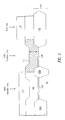
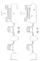
- Figure 1 illustrates one embodiment of a structure 100 comprising a silicon wafer 104 with formed insulation layers or elements 106A-106C.
- the insulators 106A-106C may be formed of any suitable insulation material, such as TEOS, and may be fabricated by either local oxidation of silicon (LOCOS) or shallow trench isolation (STI) according to the design rules of the technology.
- LOC local oxidation of silicon
- STI shallow trench isolation
- the structure 100 in Figure 1 may be used to form a CMOS integrated circuit with transistors and fuses.
- the present invention may be applied to any configuration and any number of transistors and fuses. Two transistors and a fuse are described below with reference to the Figures merely as an example.
- the sizes and thicknesses of the elements and layers shown in the Figures are not drawn to scale and are not intended to be limitations.
- CMOS process such as 0.18 ⁇ m, 0.13 ⁇ m or 0.10 ⁇ m, may be used to form the elements described below.
- One or more of the acts described below may be modified or performed in a different sequence.
- the surface of the silicon substrate 104 in Figure 1 may be cleaned with a pre-gate-oxide clean process, and a gate oxide layer 102A, 102B may be formed.
- the gate oxide layer is less than 2nm thick.
- a polysilicon layer 108 may be deposited.
- the polysilicon layer 108 has a thickness T of about 100 nm to about 150 nm, such as 120 nm or 130 nm.
- the thickness T is typically a compromise between (1) a desire for increased margin for a gate patterning process to create a narrow gate, which is facilitated by a thinner poly, and (2) a desire for high dose implants for the transistor source-drain regions, in which a thicker poly will more effectively block source-drain implanted species, particularly Boron, from penetrating the channel.
- the desire to pattern smaller transistor gates in order to raise transistor drive strength is expected to force the poly thickness T to be reduced every few technology generations.
- a poly thickness of 150 nm to 200 nm may provide adequate process latitude for the gate patterning process.
- a poly thickness of 100 nm to 120 nm may be adequate to achieve a desired process margin.
- a poly thickness of 100 nm may be adequate to achieve a desired process margin.
- the thickness T of the poly may be about 50 nm or less, such as 10 nm.
- a mask 110 (called an NMOS implant resist) may be formed for gate pre-doping. Then a pre-doping implant may be applied to a region 112 of the polysilicon layer 108. The mask 110 may be removed for further processing.
- Figure 2 illustrates the structure 100 of Figure 1 at another stage of processing, which may be after processing in Figure 1.
- a mask called a PMOS implant resist
- a pre-doping implant may be applied to a region 200 of the polysilicon layer 108.
- the mask 202 may be removed for further processing.
- Figure 3 illustrates the structure 100 of Figure 1 at another stage of processing, which may be after processing in Figure 2.
- a bottom anti-reflective coating (BARC) 304 also called a BARC film or ARC "under resist” may be formed.
- the surface of the polysilicon layer 108 ( Figure 2) may be fairly smooth and facilitate the deposition of a BARC film with a well-controlled thickness and optical properties by chemical vapor deposition (CVD), such as PECVD or LPCVD.
- CVD chemical vapor deposition
- a photoresist layer (not shown), such as a photo-sensitive plastic, may be formed on both transistor gate areas and the fuse area.
- the photoresist may be trimmed to form photoresist structures 306A, 306B, 308 as shown in Figure 3. Without the BARC 304, when the photoresist is exposed, reflections off an interface between the photoresist and the polysilicon layer will cause a resulting post-develop resist profile to be tapered rather than straight.
- portions of the BARC layer 304 and the polysilicon layer 108 in Figure 3 may be etched with a main etch process, a soft landing process and an over-etch process, if desired, to form polysilicon gate areas 310A, 310B and a polysilicon fuse area 312 shown in Figures 3 and 4.
- the polysilicon gate areas 310A, 310B in Figure 4 may have widths W3, W4 of about 50nm to 100 nm, such as 60nm or 70nm, for current technologies.
- the gate etch process is designed to prevent any punctures of the gate oxide layers 102A, 102B.
- gate etching is followed by a passivant clean process to remove etch polymer residue, a critical dimension (CD) measurement, an inspection for resist scum, a short oxidation (grows about 2 nm on active region and about 4 nm on sides of gates, and removing the BARC layer 304.
- a passivant clean process to remove etch polymer residue
- CD critical dimension
- an inspection for resist scum an inspection for resist scum
- a short oxidation (grows about 2 nm on active region and about 4 nm on sides of gates
- removing the BARC layer 304 may comprise a hot phosphoric acid clean, but plasma etches can be used as well.
- the BARC 304 may be removed much later in the process flow, as long as polysilicon in the gate areas 310A, 310B and silicon 104 in the active regions are exposed when a material such as cobalt is deposited.
- an oxidation process increases the thickness of the gate oxide layers 102A, 102B in Figure 3.
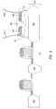
- Figure 4 illustrates the structure 100 of Figure 1 at another stage of processing, which may be after processing in Figure 3.
- transistor gate areas 310A, 310B After patterning the transistor gate areas 310A, 310B, several masking processes (used to define implant areas) and implant processes may be performed to form transistors 400A, 400B shown in Figure 4.
- Nitride spacers 402A-402F may be formed on the sides of the etched polysilicon gate areas 310A, 310B and the polysilicon fuse area 312. More implants may be performed.
- the oxide layers 102A, 102B are present and may actually be thicker than directly underneath the gate areas 400A, 400B. Portions of the oxide layers 102A, 102B in Figure 3 between the spacers 402A-402F and the insulators 106A-106C (not protected by the spacers and doped gate polysilicon areas 310A, 310B) are eventually removed, for example, by the combined effect of multiple cleaning processes at various points in the flow. Each cleaning process may remove a few angstroms of the oxide layers 102A, 102B between the spacers 402A-402F and the insulators 106A-106C, and eventually these portions of the oxide layer are removed.
- portions of the oxide layers 102A, 102B between the spacers 402A-402F and the insulators 106A-106C may be removed during nitride etching as the nitride spacers 402A-402D are formed and etched. Multiple cleaning processes between spacer definition and cobalt deposition will remove most of the remaining portions of the oxide layers 102A, 102B between the spacers 402A-402F and the insulators 106A-106C.
- a cobalt deposition recipe includes a sputter clean capable of removing about 3 nm of oxide, followed by the Co deposition, followed by a capping layer of about 5 nm of Ti or TiN.
- a cobalt layer 404 may be deposited on all elements, as shown in Figure 4.
- the cobalt layer 404 is about 150 ⁇ thick and the polysilicon layer 312 is about 1200-1500 ⁇ thick. Other thicknesses may be used in other embodiments.
- cobalt other elements may be used, such as titanium or nickel.
- RTA rapid thermal anneal
- a formation RTA process with a temperature of about 430 - 480° C and about one minute in duration forms CoSi. Then unreacted Co is stripped. Then a second formation RTA with a temperature of about 675 - 775° C and a few seconds in duration is applied to form CoSi 2 .
- a polysilicon fuse area is thinner than the polysilicon transistor gate areas, such that substantially all of the polysilicon fuse area is converted to polysilicide during one or more RTA processes.
- the polysilicon thickness and the polysilicide thickness are dictated by optimizing transistor performance and ease of 100-nm to 150-nm gate patterning processes.
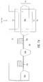
- Figure 5 illustrates the structure 100 of Figure 1 at another stage of processing, which may be after processing in Figure 2.
- a patterned mask 500 such as a photoresist for the fuse area is defined and formed.
- a polysilicon thinning etch process may be applied to the polysilicon layer 108 to form an etched fuse area 502.
- the processes described above with reference to Figures 3-4 such as resist trimming, BARC etching and polysilicon etching (main etch, soft landing, over-etch), may be modified to provide multiple polysilicon thicknesses for transistor and fuse areas.
- Figure 6 illustrates the structure 100 of Figure 1 at another stage of processing, which may be after processing in Figure 2.
- a BARC layer 304 is deposited, as in Figure 3.
- a photoresist layer is formed and trimmed to form masks 600A, 600B, 602 that are wider than the structures 306A, 306B, 308 in Figure 3.
- the structures 600A, 600B, 602 in Figure 6 protect the future polysilicon transistor gate and fuse areas 310A, 310B, 312 for later etching.
- Figure 7A illustrates the structure 100 of Figure 1 at another stage of processing, which may be after processing in Figure 6.
- a first etch process may form polysilicon transistor gate structures 310A, 310B and delineate an approximate polysilicon fuse structure 312 in Figure 7A.
- the approximate polysilicon fuse structure 312 is over-sized to provide some extra material to process an actual polysilicon fuse area 604, as shown in Figures 6 and 7A.
- the fuse mask 602 should be sufficiently wide to enclose the actual "fusing" portion 604 of the fuse. In other words, the fuse mask 602 should be wider than the electrically active portion of the fuse. Second, the fuse mask 602 should be enclosed by the poly fuse area 606 such that a poly etch process does not attack active Si. In other words, the fuse mask 602 should be narrower than the outer edges of the poly fuse area 606.
- a fuse definition mask 700 in Figure 7A may then be formed to protect the polysilicon transistor gate areas 310A, 310B. Then a thinning etch process is applied to the approximate polysilicon fuse structure 312 to remove some polysilicon material 702 and form the actual polysilicon fuse area 604. In order to facilitate a consistent manufacturable process, this thinning etch may employ interferometric end-point (IEP) techniques to terminate the etch when a specified thickness of polysilicon remains unetched. IEP is a technique available in most state-of-the-art commercial etch tools, e.g. from LAM or AMAT. Thus, separate polysilicon etches are performed for gate and fuse areas.
- IEP interferometric end-point
- CMOS processes may be applied, such as implanting, forming spacers 402A-402F ( Figure 4), more implants, cobalt deposition, CoSi formation anneal and stripping any unreacted cobalt that did not react to form CoSi.
- Figure 7B illustrates the structure of Figure 1 at another stage of processing, which may be after processing in Figure 5 or Figures 6 and 7A.
- Figure 7B shows a fresh or unprogrammed fuse area that directly contacts the insulator 106C.
- Figure 7C illustrates the structure of Figure 1 at another stage of processing, which may be after processing in Figure 5 or Figures 6 and 7A.
- Figure 7B shows a fresh or unprogrammed fuse area that is separated from the insulator 106C by an acceptably thin layer of polysilicon 750.
- the cobalt, titanium or nickel polysilicide (or silicided polysilicon) fuse layer 410 has a low resistance as current may pass from one end of the fuse layer 410 to the other end.
- the fuse may be called a fresh or pre-programmed fuse.
- the fuse may be later programmed by agglomeration, as understood by those of ordinary skill in the integrated circuit processing art. In one embodiment, the agglomeration occurs at about 1000 degrees Celsius.
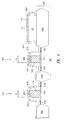
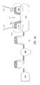
- Figure 8 illustrates a programmed fuse 800 on the structure 100 of Figure 1 at another stage of processing, which may be after processing in Figure 4.
- the programmed fuse 800 in Figure 8 has two polysilicide areas 410A, 410B on the polysilicon layer 312.
- the two polysilicide areas 410A, 410B are coupled to traces or conductors 804A, 804B.
- the two polysilicide areas 410A, 410B are separated by an agglomerated region 802, which exposes a part of the underlying polysilicon layer 312.
- the programmed fuse 800 in Figure 8 has a post-programming resistance that is higher than a pre-programming resistance because of the agglomerated region 802. But some current still flows through the polysilicon layer 312, as shown by the arrows in Figure 8.
- Figure 9A illustrates a programmed fuse 900A on the structure 100 of Figure 1 at another stage of processing, which may be after cobalt deposition, CoSi formation anneal and stripping unreacted cobalt after processing in Figure 5 or Figures 6 and 7A.
- the polysilicon fuse layer is thinner than in Figure 4 such that substantially all of the polysilicon in the fuse area in Figures 5 and 7A is consumed during silicidation (see Figure 7B).
- Figure 9B illustrates another programmed fuse 900B on the structure 100 of Figure 1 at another stage of processing, which may be after cobalt deposition, CoSi formation anneal and stripping unreacted cobalt after processing in Figure 5 or Figures 6 and 7A.
- an acceptable amount 910 of polysilicon is not consumed during silicidation (see Figure 7C), possibly to accommodate other CMOS process conditions.
- the programmed fuses 900A, 900B in Figures 9A and 9B have two polysilicide areas 902A, 902B.
- the two polysilicide areas 902A, 902B in Figure 9A contact the surface of the insulator 106C.
- the two polysilicide areas 902A, 902B in Figure 9B contact the acceptable amount 910 of polysilicon.
- the two polysilicide areas 902A, 902B in Figures 9A and 9B are coupled to plugs or conductors 906A, 906B.
- the two polysilicide areas 902A, 902B are separated by an agglomerated region 904, which exposes a part of the insulator layer 106C in Figure 9A and exposes a part of the polysilicon 910 in Figure 9B.
- the programmed fuses 900A, 900B in Figures 9A, 9B have a post-programming resistance that is much higher than a pre-programming resistance (high figure of merit) because the agglomerated region 904 exposes the insulator 106C in Figure 9A or a thin layer of polysilicon 910 in Figure 9B. There is no current flowing through the insulator 106C, as shown by the single arrow in Figure 9A. Thus, the programmed fuse 900A in Figure 9A forms an ideal open circuit (i.e., broken circuit). Similarly, there is a negligible amount of current flowing through the insulator 106C and thin polysilicon layer 910 in Figure 9B.
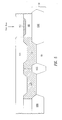
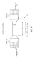
- Figure 10 is a top view of an unprogrammed fuse 1000 at another stage of processing, which may be after cobalt deposition, CoSi formation anneal and stripping unreacted cobalt after processing in Figure 5 or Figures 6 and 7A.
- the fuse length L, width W and shape of the fuse element 1000 are optimized for programming at lower voltages.
- the contact plugs 1004A, 1004B on the contact pads 1002A, 1002B are used to electrically connect the fuse element 1000 to a power supply voltage, which may be used to program the fuse 1000.
Landscapes
- Design And Manufacture Of Integrated Circuits (AREA)
- Semiconductor Memories (AREA)
- Electrodes Of Semiconductors (AREA)
- Internal Circuitry In Semiconductor Integrated Circuit Devices (AREA)
- Metal-Oxide And Bipolar Metal-Oxide Semiconductor Integrated Circuits (AREA)
Applications Claiming Priority (3)
| Application Number | Priority Date | Filing Date | Title |
|---|---|---|---|
| US14064 | 1998-01-27 | ||
| US10/014,064 US6756255B1 (en) | 2001-12-10 | 2001-12-10 | CMOS process with an integrated, high performance, silicide agglomeration fuse |
| PCT/US2002/039482 WO2003050858A1 (en) | 2001-12-10 | 2002-12-09 | Cmos process with an integrated, high performance, silicide agglomeration fuse |
Publications (2)
| Publication Number | Publication Date |
|---|---|
| EP1451860A1 EP1451860A1 (en) | 2004-09-01 |
| EP1451860B1 true EP1451860B1 (en) | 2008-01-16 |
Family
ID=21763328
Family Applications (1)
| Application Number | Title | Priority Date | Filing Date |
|---|---|---|---|
| EP02804766A Expired - Lifetime EP1451860B1 (en) | 2001-12-10 | 2002-12-09 | Cmos process with an integrated, high performance, silicide agglomeration fuse |
Country Status (9)
| Country | Link |
|---|---|
| US (1) | US6756255B1 (enExample) |
| EP (1) | EP1451860B1 (enExample) |
| JP (1) | JP4651941B2 (enExample) |
| KR (1) | KR100957601B1 (enExample) |
| CN (1) | CN100352009C (enExample) |
| AU (1) | AU2002357140A1 (enExample) |
| DE (1) | DE60224712T2 (enExample) |
| TW (1) | TWI270961B (enExample) |
| WO (1) | WO2003050858A1 (enExample) |
Families Citing this family (13)
| Publication number | Priority date | Publication date | Assignee | Title |
|---|---|---|---|---|
| US20050124097A1 (en) * | 2003-12-05 | 2005-06-09 | Advanced Micro Devices, Inc | Integrated circuit with two phase fuse material and method of using and making same |
| US7645687B2 (en) * | 2005-01-20 | 2010-01-12 | Chartered Semiconductor Manufacturing, Ltd. | Method to fabricate variable work function gates for FUSI devices |
| KR101211213B1 (ko) * | 2005-08-31 | 2012-12-11 | 인터내셔널 비지네스 머신즈 코포레이션 | 전기적으로 프로그램가능한 랜덤 액세스 e-퓨즈 롬 |
| US7460003B2 (en) * | 2006-03-09 | 2008-12-02 | International Business Machines Corporation | Electronic fuse with conformal fuse element formed over a freestanding dielectric spacer |
| US7288804B2 (en) * | 2006-03-09 | 2007-10-30 | International Business Machines Corporation | Electrically programmable π-shaped fuse structures and methods of fabrication thereof |
| US7784009B2 (en) * | 2006-03-09 | 2010-08-24 | International Business Machines Corporation | Electrically programmable π-shaped fuse structures and design process therefore |
| US7417300B2 (en) | 2006-03-09 | 2008-08-26 | International Business Machines Corporation | Electrically programmable fuse structures with narrowed width regions configured to enhance current crowding and methods of fabrication thereof |
| US7645645B2 (en) * | 2006-03-09 | 2010-01-12 | International Business Machines Corporation | Electrically programmable fuse structures with terminal portions residing at different heights, and methods of fabrication thereof |
| US7924597B2 (en) * | 2007-10-31 | 2011-04-12 | Hewlett-Packard Development Company, L.P. | Data storage in circuit elements with changed resistance |
| US8354304B2 (en) * | 2008-12-05 | 2013-01-15 | Stats Chippac, Ltd. | Semiconductor device and method of forming conductive posts embedded in photosensitive encapsulant |
| WO2011024340A1 (ja) * | 2009-08-27 | 2011-03-03 | パナソニック株式会社 | 半導体装置及びその製造方法 |
| US8912626B2 (en) | 2011-01-25 | 2014-12-16 | International Business Machines Corporation | eFuse and method of fabrication |
| US12408563B1 (en) * | 2020-08-24 | 2025-09-02 | Synopsys, Inc. | Superconducting anti-fuse based field programmable gate array |
Family Cites Families (15)
| Publication number | Priority date | Publication date | Assignee | Title |
|---|---|---|---|---|
| US4042950A (en) * | 1976-03-01 | 1977-08-16 | Advanced Micro Devices, Inc. | Platinum silicide fuse links for integrated circuit devices |
| JPS60261154A (ja) * | 1984-06-08 | 1985-12-24 | Hitachi Micro Comput Eng Ltd | 半導体集積回路装置の製造方法 |
| US4647340A (en) * | 1986-03-31 | 1987-03-03 | Ncr Corporation | Programmable read only memory using a tungsten fuse |
| JPH0424945A (ja) * | 1990-05-16 | 1992-01-28 | Seiko Instr Inc | 半導体装置の製造方法 |
| US5708291A (en) * | 1995-09-29 | 1998-01-13 | Intel Corporation | Silicide agglomeration fuse device |
| US6337507B1 (en) * | 1995-09-29 | 2002-01-08 | Intel Corporation | Silicide agglomeration fuse device with notches to enhance programmability |
| US5821160A (en) * | 1996-06-06 | 1998-10-13 | Motorola, Inc. | Method for forming a laser alterable fuse area of a memory cell using an etch stop layer |
| US5976943A (en) * | 1996-12-27 | 1999-11-02 | Vlsi Technology, Inc. | Method for bi-layer programmable resistor |
| FR2760563A1 (fr) * | 1997-03-07 | 1998-09-11 | Sgs Thomson Microelectronics | Pseudofusible et application a un circuit d'etablissement d'une bascule a la mise sous tension |
| US6022775A (en) | 1998-08-17 | 2000-02-08 | Taiwan Semiconductor Manufacturing Company | High effective area capacitor for high density DRAM circuits using silicide agglomeration |
| US6242790B1 (en) | 1999-08-30 | 2001-06-05 | Advanced Micro Devices, Inc. | Using polysilicon fuse for IC programming |
| JP2001077050A (ja) * | 1999-08-31 | 2001-03-23 | Toshiba Corp | 半導体装置の製造方法 |
| US6391767B1 (en) * | 2000-02-11 | 2002-05-21 | Advanced Micro Devices, Inc. | Dual silicide process to reduce gate resistance |
| JP2001326242A (ja) * | 2000-05-16 | 2001-11-22 | Matsushita Electric Ind Co Ltd | 半導体装置およびその製造方法 |
| US6642601B2 (en) * | 2000-12-18 | 2003-11-04 | Texas Instruments Incorporated | Low current substantially silicide fuse for integrated circuits |
-
2001
- 2001-12-10 US US10/014,064 patent/US6756255B1/en not_active Expired - Lifetime
-
2002
- 2002-12-09 KR KR1020047008979A patent/KR100957601B1/ko not_active Expired - Fee Related
- 2002-12-09 EP EP02804766A patent/EP1451860B1/en not_active Expired - Lifetime
- 2002-12-09 CN CNB02824656XA patent/CN100352009C/zh not_active Expired - Fee Related
- 2002-12-09 JP JP2003551823A patent/JP4651941B2/ja not_active Expired - Fee Related
- 2002-12-09 DE DE60224712T patent/DE60224712T2/de not_active Expired - Lifetime
- 2002-12-09 AU AU2002357140A patent/AU2002357140A1/en not_active Abandoned
- 2002-12-09 WO PCT/US2002/039482 patent/WO2003050858A1/en not_active Ceased
- 2002-12-10 TW TW091135639A patent/TWI270961B/zh not_active IP Right Cessation
Also Published As
| Publication number | Publication date |
|---|---|
| WO2003050858A1 (en) | 2003-06-19 |
| US6756255B1 (en) | 2004-06-29 |
| TW200301549A (en) | 2003-07-01 |
| KR20040064302A (ko) | 2004-07-16 |
| TWI270961B (en) | 2007-01-11 |
| DE60224712D1 (de) | 2008-03-06 |
| KR100957601B1 (ko) | 2010-05-13 |
| CN100352009C (zh) | 2007-11-28 |
| JP2005513764A (ja) | 2005-05-12 |
| EP1451860A1 (en) | 2004-09-01 |
| CN1695232A (zh) | 2005-11-09 |
| AU2002357140A1 (en) | 2003-06-23 |
| DE60224712T2 (de) | 2009-01-29 |
| JP4651941B2 (ja) | 2011-03-16 |
Similar Documents
| Publication | Publication Date | Title |
|---|---|---|
| CN101300677B (zh) | 电可编程熔丝及其制造方法 | |
| US8865542B2 (en) | Embedded polysilicon resistor in integrated circuits formed by a replacement gate process | |
| US6274469B1 (en) | Process using a plug as a mask for a gate | |
| US7163853B2 (en) | Method of manufacturing a capacitor and a metal gate on a semiconductor device | |
| EP1451860B1 (en) | Cmos process with an integrated, high performance, silicide agglomeration fuse | |
| KR100698501B1 (ko) | 산화 가스에 의한 급속 열 어닐링을 이용하는 바닥부 반사방지 코팅 | |
| US6258648B1 (en) | Selective salicide process by reformation of silicon nitride sidewall spacers | |
| US20100148262A1 (en) | Resistors and Methods of Manufacture Thereof | |
| US7919367B2 (en) | Method to increase charge retention of non-volatile memory manufactured in a single-gate logic process | |
| KR20100089781A (ko) | 반도체 소자내의 임베디드 저항 소자의 형성 방법 | |
| EP1091414A2 (en) | MOSFET with tapered gate and method of manufacturing it | |
| CN101621030B (zh) | 具有多晶硅接触的自对准mos结构 | |
| US20110059604A1 (en) | Methods for fabricating step gate electrode structures for field-effect transistors | |
| US8236693B2 (en) | Methods of forming silicides of different thicknesses on different structures | |
| US6559059B2 (en) | Method for fabricating a MOS transistor of an embedded memory | |
| US20070296054A1 (en) | Fuse with silicon nitride removed from fuse surface in cutting region | |
| US6756254B2 (en) | Integrated circuit having an antifuse and a method of manufacture | |
| US6617216B1 (en) | Quasi-damascene gate, self-aligned source/drain methods for fabricating devices | |
| US6268241B1 (en) | Method of forming a self-aligned silicide structure in integrated circuit fabrication | |
| US20020132458A1 (en) | Method for fabricating a MOS transistor of an embedded memory | |
| WO2003017340A2 (en) | A method for concurrent fabrication of a double polysilicon bipolar transistor and a base polysilicon resistor | |
| JP2000040819A (ja) | 半導体装置の製造方法 | |
| KR20040006476A (ko) | 화학적기계적연마를 이용한 선택적 실리사이드 형성 방법 |
Legal Events
| Date | Code | Title | Description |
|---|---|---|---|
| PUAI | Public reference made under article 153(3) epc to a published international application that has entered the european phase |
Free format text: ORIGINAL CODE: 0009012 |
|
| 17P | Request for examination filed |
Effective date: 20040514 |
|
| AK | Designated contracting states |
Kind code of ref document: A1 Designated state(s): AT BE BG CH CY CZ DE DK EE ES FI FR GB GR IE IT LI LU MC NL PT SE SI SK TR |
|
| AX | Request for extension of the european patent |
Extension state: AL LT LV MK RO |
|
| GRAP | Despatch of communication of intention to grant a patent |
Free format text: ORIGINAL CODE: EPIDOSNIGR1 |
|
| GRAS | Grant fee paid |
Free format text: ORIGINAL CODE: EPIDOSNIGR3 |
|
| GRAA | (expected) grant |
Free format text: ORIGINAL CODE: 0009210 |
|
| AK | Designated contracting states |
Kind code of ref document: B1 Designated state(s): DE GB |
|
| REG | Reference to a national code |
Ref country code: GB Ref legal event code: FG4D |
|
| REF | Corresponds to: |
Ref document number: 60224712 Country of ref document: DE Date of ref document: 20080306 Kind code of ref document: P |
|
| PLBE | No opposition filed within time limit |
Free format text: ORIGINAL CODE: 0009261 |
|
| STAA | Information on the status of an ep patent application or granted ep patent |
Free format text: STATUS: NO OPPOSITION FILED WITHIN TIME LIMIT |
|
| 26N | No opposition filed |
Effective date: 20081017 |
|
| REG | Reference to a national code |
Ref country code: GB Ref legal event code: 732E Free format text: REGISTERED BETWEEN 20091210 AND 20091216 |
|
| PGFP | Annual fee paid to national office [announced via postgrant information from national office to epo] |
Ref country code: GB Payment date: 20101123 Year of fee payment: 9 |
|
| PGFP | Annual fee paid to national office [announced via postgrant information from national office to epo] |
Ref country code: DE Payment date: 20101230 Year of fee payment: 9 |
|
| GBPC | Gb: european patent ceased through non-payment of renewal fee |
Effective date: 20111209 |
|
| PG25 | Lapsed in a contracting state [announced via postgrant information from national office to epo] |
Ref country code: GB Free format text: LAPSE BECAUSE OF NON-PAYMENT OF DUE FEES Effective date: 20111209 |
|
| REG | Reference to a national code |
Ref country code: DE Ref legal event code: R119 Ref document number: 60224712 Country of ref document: DE Effective date: 20130702 |
|
| PG25 | Lapsed in a contracting state [announced via postgrant information from national office to epo] |
Ref country code: DE Free format text: LAPSE BECAUSE OF NON-PAYMENT OF DUE FEES Effective date: 20130702 |