EP1450418A2 - Flächenlichtquelle, Herstellungsverfahren dafür und Flüssigkristallanzeigeeinheit - Google Patents
Flächenlichtquelle, Herstellungsverfahren dafür und Flüssigkristallanzeigeeinheit Download PDFInfo
- Publication number
- EP1450418A2 EP1450418A2 EP04003656A EP04003656A EP1450418A2 EP 1450418 A2 EP1450418 A2 EP 1450418A2 EP 04003656 A EP04003656 A EP 04003656A EP 04003656 A EP04003656 A EP 04003656A EP 1450418 A2 EP1450418 A2 EP 1450418A2
- Authority
- EP
- European Patent Office
- Prior art keywords
- transparent substrate
- exit surface
- light emitting
- emitting device
- light exit
- Prior art date
- Legal status (The legal status is an assumption and is not a legal conclusion. Google has not performed a legal analysis and makes no representation as to the accuracy of the status listed.)
- Withdrawn
Links
Images

Classifications
-
- A—HUMAN NECESSITIES
- A61—MEDICAL OR VETERINARY SCIENCE; HYGIENE
- A61H—PHYSICAL THERAPY APPARATUS, e.g. DEVICES FOR LOCATING OR STIMULATING REFLEX POINTS IN THE BODY; ARTIFICIAL RESPIRATION; MASSAGE; BATHING DEVICES FOR SPECIAL THERAPEUTIC OR HYGIENIC PURPOSES OR SPECIFIC PARTS OF THE BODY
- A61H23/00—Percussion or vibration massage, e.g. using supersonic vibration; Suction-vibration massage; Massage with moving diaphragms
- A61H23/02—Percussion or vibration massage, e.g. using supersonic vibration; Suction-vibration massage; Massage with moving diaphragms with electric or magnetic drive
-
- G—PHYSICS
- G02—OPTICS
- G02F—OPTICAL DEVICES OR ARRANGEMENTS FOR THE CONTROL OF LIGHT BY MODIFICATION OF THE OPTICAL PROPERTIES OF THE MEDIA OF THE ELEMENTS INVOLVED THEREIN; NON-LINEAR OPTICS; FREQUENCY-CHANGING OF LIGHT; OPTICAL LOGIC ELEMENTS; OPTICAL ANALOGUE/DIGITAL CONVERTERS
- G02F1/00—Devices or arrangements for the control of the intensity, colour, phase, polarisation or direction of light arriving from an independent light source, e.g. switching, gating or modulating; Non-linear optics
- G02F1/01—Devices or arrangements for the control of the intensity, colour, phase, polarisation or direction of light arriving from an independent light source, e.g. switching, gating or modulating; Non-linear optics for the control of the intensity, phase, polarisation or colour
- G02F1/13—Devices or arrangements for the control of the intensity, colour, phase, polarisation or direction of light arriving from an independent light source, e.g. switching, gating or modulating; Non-linear optics for the control of the intensity, phase, polarisation or colour based on liquid crystals, e.g. single liquid crystal display cells
- G02F1/133—Constructional arrangements; Operation of liquid crystal cells; Circuit arrangements
- G02F1/1333—Constructional arrangements; Manufacturing methods
- G02F1/1335—Structural association of cells with optical devices, e.g. polarisers or reflectors
- G02F1/1336—Illuminating devices
- G02F1/133602—Direct backlight
- G02F1/133603—Direct backlight with LEDs
-
- A—HUMAN NECESSITIES
- A61—MEDICAL OR VETERINARY SCIENCE; HYGIENE
- A61H—PHYSICAL THERAPY APPARATUS, e.g. DEVICES FOR LOCATING OR STIMULATING REFLEX POINTS IN THE BODY; ARTIFICIAL RESPIRATION; MASSAGE; BATHING DEVICES FOR SPECIAL THERAPEUTIC OR HYGIENIC PURPOSES OR SPECIFIC PARTS OF THE BODY
- A61H23/00—Percussion or vibration massage, e.g. using supersonic vibration; Suction-vibration massage; Massage with moving diaphragms
- A61H23/006—Percussion or tapping massage
-
- A—HUMAN NECESSITIES
- A61—MEDICAL OR VETERINARY SCIENCE; HYGIENE
- A61H—PHYSICAL THERAPY APPARATUS, e.g. DEVICES FOR LOCATING OR STIMULATING REFLEX POINTS IN THE BODY; ARTIFICIAL RESPIRATION; MASSAGE; BATHING DEVICES FOR SPECIAL THERAPEUTIC OR HYGIENIC PURPOSES OR SPECIFIC PARTS OF THE BODY
- A61H39/00—Devices for locating or stimulating specific reflex points of the body for physical therapy, e.g. acupuncture
- A61H39/04—Devices for pressing such points, e.g. Shiatsu or Acupressure
-
- H—ELECTRICITY
- H10—SEMICONDUCTOR DEVICES; ELECTRIC SOLID-STATE DEVICES NOT OTHERWISE PROVIDED FOR
- H10K—ORGANIC ELECTRIC SOLID-STATE DEVICES
- H10K50/00—Organic light-emitting devices
- H10K50/80—Constructional details
- H10K50/85—Arrangements for extracting light from the devices
-
- A—HUMAN NECESSITIES
- A61—MEDICAL OR VETERINARY SCIENCE; HYGIENE
- A61H—PHYSICAL THERAPY APPARATUS, e.g. DEVICES FOR LOCATING OR STIMULATING REFLEX POINTS IN THE BODY; ARTIFICIAL RESPIRATION; MASSAGE; BATHING DEVICES FOR SPECIAL THERAPEUTIC OR HYGIENIC PURPOSES OR SPECIFIC PARTS OF THE BODY
- A61H2205/00—Devices for specific parts of the body
- A61H2205/02—Head
-
- H—ELECTRICITY
- H10—SEMICONDUCTOR DEVICES; ELECTRIC SOLID-STATE DEVICES NOT OTHERWISE PROVIDED FOR
- H10K—ORGANIC ELECTRIC SOLID-STATE DEVICES
- H10K50/00—Organic light-emitting devices
- H10K50/80—Constructional details
Definitions
- the present invention relates to an area light emitting device emitting light through an area, a method for manufacturing such a light emitting device, and a liquid crystal display unit having such a light emitting device.
- a typical area light emitting device has an area light emitting element emitting light through an area. Light from such an area light emitting element is emitted through a flat substrate. In this case, only 20 to 25% of light from the light emitting element exits the light emitting device. That is, the light emitting device is unable to efficiently emit light emitted from the light emitting element. This is because a great proportion of light from the light emitting element is reflected on an interface between the flat substrate and air.
- a plano-convex lens is formed in each section of a substrate that corresponds to a pixel, thereby increasing the proportion of light that exits the organic EL device.
- light scatterers which are asperities formed by etching a transparent film, are provided on a substrate to increase the proportion of light that exits the light emitting device.
- an objective of the present invention to provide a novel area light emitting device that is capable of efficiently emitting light emitted from a light emitting element, and a method for manufacturing such an area light emitting device.
- Another objective of the present invention is to provide a liquid crystal display unit provided with such an area light emitting device.
- an area light emitting device includes a transparent substrate having a predetermined thickness and an area light emitting element provided on the transparent substrate.
- the transparent substrate includes a light exit surface. Light emitted from the element advances through the transparent substrate and exits the device through the light exit surface.
- a plurality of recesses are located on the light exit surface. A part of the light exit surface between each adjacent pair of the recesses includes a plane that is perpendicular to the thickness direction of the transparent substrate.
- the present invention also provides another area light emitting device.
- the device includes a transparent substrate and an area light emitting element provided on the transparent substrate.
- the transparent substrate includes a light exit surface. Light emitted from the element advances through the transparent substrate and exits the device through the light exit surface.
- a plurality of recesses are located on the light exit surface. The recesses are formed by processing the light exit surface. A part of the light exit surface between each adjacent pair of the recesses includes a portion that is not subjected to the process for forming the recesses.
- a method for manufacturing an area light emitting device includes a transparent substrate and an area light emitting element provided on the transparent substrate.
- the transparent substrate includes a light exit surface. Light emitted from the element advances through the transparent substrate and exits the device through the light exit surface.
- the method includes: masking a part of the light exit surface with a mask; sandblasting the light exit surface, which is masked, thereby forming a plurality of recesses in the light exit surface; and removing the mask after the sandblasting.
- the present invention provides another method for manufacturing an area light emitting device.
- the device includes a transparent substrate and an organic electroluminescent element.
- the transparent substrate includes a light exit surface. Light emitted from the element advances through the transparent substrate and exits the device through the light exit surface.
- the method includes: forming the organic electroluminescent element on the transparent substrate; sealing the organic electroluminescent element on the transparent substrate; masking a part of the light exit surface of the transparent substrate, on which the organic electroluminescent element is formed, with a mask; sandblasting the light exit surface, which is masked, thereby forming a plurality of recesses in the light exit surface; and removing the mask after the sandblasting.
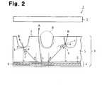
- Figs. 1(a) and 2 show a transmissive liquid crystal display unit 1 that includes a liquid crystal member and an area light emitting device.
- the liquid crystal member is a liquid crystal panel 2
- the area light emitting device is a backlight 3.
- the liquid crystal panel 2 has a conventional configuration, and, for example, includes pixels arranged in a matrix. Each pixel has color filters of red, blue and green.
- the liquid crystal panel 2 creates an image using the pixels.
- the backlight 3 is formed of a transparent substrate 5, and an organic electroluminescent element 4, which is an area light emitting element provided on the transparent substrate 5.
- the transparent substrate 5 is made of glass and has a thickness of 500 ⁇ m.
- the transparent substrate 5 permits part of or all visible light to pass through.
- the transparent substrate 5 has an incidence surface 6 and a light exit surface 7, which are located at opposite sides of the transparent substrate 5 with respect to each other.
- the incidence surface 6 is contained in the interface between the organic electroluminescent element 4 and the transparent substrate 5.
- the light exit surface 7 is contained in the interface between the transparent substrate 5 and the air.
- the incidence surface 6 is flat and faces the organic electroluminescent element 4.
- the light exit surface 7 faces away from the organic electroluminescent element 4, and is uneven with regularly arranged recesses 8. A part of the light exit surface 7 where no recesses 8 are formed is perpendicular to the thickness direction of the transparent substrate 5 and parallel to the incidence surface 6.
- the recesses 8 have the same semi-spheroidal shape in the same size. As shown in Fig. 1(b), each recess 8 has a circular opening. The diameter of the opening and the depth of the recess 8 are both 250 ⁇ m. Except for the recesses 8 located at the periphery of the light exit surface 7, each recess 8 is surrounded by other six recesses 8. Each adjacent pair of the recesses 8 is spaced by 50 ⁇ m.
- the recesses 8 are formed in the following manner. First, the transparent substrate 5, on which the organic electroluminescent element 4 is formed, is prepared. Before the recesses 8 are formed, the light exit surface 7 is perpendicular to the thickness direction of the transparent substrate 5 and parallel to the incidence surface 6. To prevent the organic electroluminescent element 4 from being scratched, the organic electroluminescent element 4 is sealed with a sealing member (not shown). Then, a part of the light exit surface 7 other than sections corresponding to the recesses 8 is protected with a mask. In this state, the light exit surface 7 is sandblasted. Accordingly, the portions of the light exit surface 7 that are not protected with the mask are ground so that the recesses 8 are formed. The mask is removed after the sandblasting.
- each section of the light exit surface 7 between an adjacent pair of the recesses 8 is not ground with sandblasting media, and stays perpendicular to the thickness direction of the transparent substrate 5 and parallel to the incidence surface 6.
- the organic electroluminescent element 4 includes a flat transparent electrode made of indium tin oxide (ITO), an organic layer including a flat light emitting layer 9, and a flat metal electrode, which are subsequently formed on the transparent substrate 5.
- ITO indium tin oxide
- the entire light emitting layer 9 of the organic electroluminescent element 4 simultaneously emit light of the same color.
- the light emitting layer 9 emits white light.
- Light emitted from the light emitting layer 9 advances to the transparent substrate 5 through the incidence surface 6 and then advances to the outside of the transparent substrate 5 through the light exit surface 7.
- the backlight 3 emits light emitted from the organic electroluminescent element 4 through the light exit surface 7.
- emission points on the organic electroluminescent element 4 are assumed to continuously exist on a plane parallel to the incidence surface 6 of the transparent substrate 5. Each emission point emits light evenly in all directions. Therefore, light emitted from the light emitting layer 9 enters the incidence surface 6 at every angle.
- An arrow A in Fig. 2 represents a ray of a portion of light from the back of the incidence surface 6.
- the emission angle of the ray of the arrow A is less than the critical angle at the interface between the transparent substrate 5 and air. If the ray of the arrow A reaches the back of the light exit surface 7 where no recesses 8 are formed, the ray is not totally reflected on the interface between the transparent substrate 5 and air and exits the substrate 5 through the light exit surface 7.
- Arrows B in Fig. 2 represent rays of portions of light from the back of the incidence surface 6.
- the emission angles of the rays of the arrows B are equal to or greater than the critical angle at the interface between the transparent substrate 5 and air. If the rays of the arrows B reach the back of the light exit surface 7 where no recesses 8 are formed, the rays are totally reflected on the interface between the transparent substrate 5 and air and does not exit the substrate 5 through the light exit surface 7. However, depending on the conditions, the rays represented by the arrows B, which reach the back of the light exit surface 7 where the recesses 8 are formed, are not totally reflected on the interface between the transparent substrate 5 and air but exit the substrate 5 through the light exit surface 7.
- This embodiment provides the following advantages.
- the area light emitting device forming the backlight 3, or the organic electroluminescent element 4, may be replaced by an inorganic electroluminescent element. This modification also has the advantages of the illustrated embodiment.
- the recesses 8 are formed in the transparent substrate 5, which has been formed as a flat plate.
- the recesses 8 may be formed at the same time when the transparent substrate 5 is molded using a mold. This modification also has the advantages of the illustrated embodiment.
- the recesses 8 are formed through sandblasting.
- the recesses 8 may be formed through etching. This modification also has the advantages of the illustrated embodiment.
- photolithography is typically employed.
- the formation of the recesses 8 through photolithography is more complicated than a method using sandblasting.
- the area light emitting device is used as the backlight 3 of the liquid crystal display unit 1.
- the area light emitting device may be applied to other purposes such as lighting devices. This modification also has the advantages of the illustrated embodiment.
- the color of light emitted by the organic electroluminescent element 4 need not be white, but may be any color. This modification also has the advantages of the illustrated embodiment.
- the transparent substrate 5 need not be made of glass, but may be made of a resin. This modification also has the advantages of the illustrated embodiment.
- a backlight in a liquid crystal display unit has a transparent substrate and an organic electroluminescent element provided on the transparent substrate.
- the backlight emits light emitted from the organic electroluminescent element from a light exit surface of the transparent substrate.
- a plurality of recesses are formed in the light exit surface. A part of the light exit surface between each adjacent pair of the recesses includes a plane that is perpendicular to the thickness direction of the transparent substrate. The backlight permits light emitted from the organic electroluminescent element to be efficiently emitted.
Applications Claiming Priority (2)
| Application Number | Priority Date | Filing Date | Title |
|---|---|---|---|
| JP2003040632A JP2004253199A (ja) | 2003-02-19 | 2003-02-19 | 面状発光装置、その製造方法、及び液晶表示装置 |
| JP2003040632 | 2003-02-19 |
Publications (1)
| Publication Number | Publication Date |
|---|---|
| EP1450418A2 true EP1450418A2 (de) | 2004-08-25 |
Family
ID=32732933
Family Applications (1)
| Application Number | Title | Priority Date | Filing Date |
|---|---|---|---|
| EP04003656A Withdrawn EP1450418A2 (de) | 2003-02-19 | 2004-02-18 | Flächenlichtquelle, Herstellungsverfahren dafür und Flüssigkristallanzeigeeinheit |
Country Status (6)
| Country | Link |
|---|---|
| US (1) | US20040160787A1 (de) |
| EP (1) | EP1450418A2 (de) |
| JP (1) | JP2004253199A (de) |
| KR (1) | KR100587746B1 (de) |
| CN (1) | CN1525798A (de) |
| TW (1) | TWI245584B (de) |
Cited By (20)
| Publication number | Priority date | Publication date | Assignee | Title |
|---|---|---|---|---|
| WO2006036496A1 (en) * | 2004-09-27 | 2006-04-06 | Idc, Llc | Optical films for directing light towards active areas of displays |
| US7349141B2 (en) | 2004-09-27 | 2008-03-25 | Idc, Llc | Method and post structures for interferometric modulation |
| US7706050B2 (en) | 2004-03-05 | 2010-04-27 | Qualcomm Mems Technologies, Inc. | Integrated modulator illumination |
| US7710632B2 (en) | 2004-09-27 | 2010-05-04 | Qualcomm Mems Technologies, Inc. | Display device having an array of spatial light modulators with integrated color filters |
| US7750886B2 (en) | 2004-09-27 | 2010-07-06 | Qualcomm Mems Technologies, Inc. | Methods and devices for lighting displays |
| US7766498B2 (en) | 2006-06-21 | 2010-08-03 | Qualcomm Mems Technologies, Inc. | Linear solid state illuminator |
| US7807488B2 (en) | 2004-09-27 | 2010-10-05 | Qualcomm Mems Technologies, Inc. | Display element having filter material diffused in a substrate of the display element |
| US7813026B2 (en) | 2004-09-27 | 2010-10-12 | Qualcomm Mems Technologies, Inc. | System and method of reducing color shift in a display |
| US7949213B2 (en) | 2007-12-07 | 2011-05-24 | Qualcomm Mems Technologies, Inc. | Light illumination of displays with front light guide and coupling elements |
| US8040588B2 (en) | 2004-09-27 | 2011-10-18 | Qualcomm Mems Technologies, Inc. | System and method of illuminating interferometric modulators using backlighting |
| US8045252B2 (en) | 2004-02-03 | 2011-10-25 | Qualcomm Mems Technologies, Inc. | Spatial light modulator with integrated optical compensation structure |
| US8049951B2 (en) | 2008-04-15 | 2011-11-01 | Qualcomm Mems Technologies, Inc. | Light with bi-directional propagation |
| US8172417B2 (en) | 2009-03-06 | 2012-05-08 | Qualcomm Mems Technologies, Inc. | Shaped frontlight reflector for use with display |
| US8538665B2 (en) | 2008-04-24 | 2013-09-17 | Continental Automotive Gmbh | Control circuit for an electrochemical gas sensor and method for adjusting an electrochemical gas sensor |
| US8798425B2 (en) | 2007-12-07 | 2014-08-05 | Qualcomm Mems Technologies, Inc. | Decoupled holographic film and diffuser |
| US8848294B2 (en) | 2010-05-20 | 2014-09-30 | Qualcomm Mems Technologies, Inc. | Method and structure capable of changing color saturation |
| US8872085B2 (en) | 2006-10-06 | 2014-10-28 | Qualcomm Mems Technologies, Inc. | Display device having front illuminator with turning features |
| US8979349B2 (en) | 2009-05-29 | 2015-03-17 | Qualcomm Mems Technologies, Inc. | Illumination devices and methods of fabrication thereof |
| US9019183B2 (en) | 2006-10-06 | 2015-04-28 | Qualcomm Mems Technologies, Inc. | Optical loss structure integrated in an illumination apparatus |
| US9025235B2 (en) | 2002-12-25 | 2015-05-05 | Qualcomm Mems Technologies, Inc. | Optical interference type of color display having optical diffusion layer between substrate and electrode |
Families Citing this family (6)
| Publication number | Priority date | Publication date | Assignee | Title |
|---|---|---|---|---|
| KR100781616B1 (ko) * | 2006-04-07 | 2007-12-05 | 네오뷰코오롱 주식회사 | 유리 절연막을 포함하는 디스플레이 장치와 유리 절연막을제조하는 방법 및 유리 절연막을 이용하는 유기전계발광소자의 제조방법 |
| CN100437154C (zh) * | 2007-03-13 | 2008-11-26 | 友达光电股份有限公司 | 光源扩散板及背光模块 |
| JP2010040211A (ja) * | 2008-07-31 | 2010-02-18 | Sumitomo Chemical Co Ltd | 有機エレクトロルミネッセンス素子、その製造方法、照明装置、面状光源、および表示装置 |
| JP2010219006A (ja) * | 2009-03-19 | 2010-09-30 | Toppan Printing Co Ltd | El素子、バックライト装置、照明装置、電子看板装置並びにディスプレイ装置 |
| US8687145B2 (en) | 2010-08-13 | 2014-04-01 | Lg Chem, Ltd. | Organic electroluminescent device and method for fabricating the same |
| KR102516687B1 (ko) * | 2015-09-30 | 2023-03-30 | 엘지디스플레이 주식회사 | 반사 제어 필름과 이를 포함하는 디스플레이 장치 |
Family Cites Families (1)
| Publication number | Priority date | Publication date | Assignee | Title |
|---|---|---|---|---|
| JP2001004998A (ja) * | 1999-06-24 | 2001-01-12 | Nec Corp | 液晶表示装置 |
-
2003
- 2003-02-19 JP JP2003040632A patent/JP2004253199A/ja active Pending
-
2004
- 2004-02-12 KR KR1020040009347A patent/KR100587746B1/ko not_active IP Right Cessation
- 2004-02-13 US US10/778,962 patent/US20040160787A1/en not_active Abandoned
- 2004-02-16 TW TW093103584A patent/TWI245584B/zh not_active IP Right Cessation
- 2004-02-18 CN CNA2004100283168A patent/CN1525798A/zh active Pending
- 2004-02-18 EP EP04003656A patent/EP1450418A2/de not_active Withdrawn
Cited By (25)
| Publication number | Priority date | Publication date | Assignee | Title |
|---|---|---|---|---|
| US9025235B2 (en) | 2002-12-25 | 2015-05-05 | Qualcomm Mems Technologies, Inc. | Optical interference type of color display having optical diffusion layer between substrate and electrode |
| US9019590B2 (en) | 2004-02-03 | 2015-04-28 | Qualcomm Mems Technologies, Inc. | Spatial light modulator with integrated optical compensation structure |
| US8111445B2 (en) | 2004-02-03 | 2012-02-07 | Qualcomm Mems Technologies, Inc. | Spatial light modulator with integrated optical compensation structure |
| US8045252B2 (en) | 2004-02-03 | 2011-10-25 | Qualcomm Mems Technologies, Inc. | Spatial light modulator with integrated optical compensation structure |
| US7880954B2 (en) | 2004-03-05 | 2011-02-01 | Qualcomm Mems Technologies, Inc. | Integrated modulator illumination |
| US7706050B2 (en) | 2004-03-05 | 2010-04-27 | Qualcomm Mems Technologies, Inc. | Integrated modulator illumination |
| US7710632B2 (en) | 2004-09-27 | 2010-05-04 | Qualcomm Mems Technologies, Inc. | Display device having an array of spatial light modulators with integrated color filters |
| US7807488B2 (en) | 2004-09-27 | 2010-10-05 | Qualcomm Mems Technologies, Inc. | Display element having filter material diffused in a substrate of the display element |
| US7813026B2 (en) | 2004-09-27 | 2010-10-12 | Qualcomm Mems Technologies, Inc. | System and method of reducing color shift in a display |
| WO2006036496A1 (en) * | 2004-09-27 | 2006-04-06 | Idc, Llc | Optical films for directing light towards active areas of displays |
| US7750886B2 (en) | 2004-09-27 | 2010-07-06 | Qualcomm Mems Technologies, Inc. | Methods and devices for lighting displays |
| US8040588B2 (en) | 2004-09-27 | 2011-10-18 | Qualcomm Mems Technologies, Inc. | System and method of illuminating interferometric modulators using backlighting |
| US7719747B2 (en) | 2004-09-27 | 2010-05-18 | Qualcomm Mems Technologies, Inc. | Method and post structures for interferometric modulation |
| US7349141B2 (en) | 2004-09-27 | 2008-03-25 | Idc, Llc | Method and post structures for interferometric modulation |
| US7766498B2 (en) | 2006-06-21 | 2010-08-03 | Qualcomm Mems Technologies, Inc. | Linear solid state illuminator |
| US8872085B2 (en) | 2006-10-06 | 2014-10-28 | Qualcomm Mems Technologies, Inc. | Display device having front illuminator with turning features |
| US9019183B2 (en) | 2006-10-06 | 2015-04-28 | Qualcomm Mems Technologies, Inc. | Optical loss structure integrated in an illumination apparatus |
| US8798425B2 (en) | 2007-12-07 | 2014-08-05 | Qualcomm Mems Technologies, Inc. | Decoupled holographic film and diffuser |
| US7949213B2 (en) | 2007-12-07 | 2011-05-24 | Qualcomm Mems Technologies, Inc. | Light illumination of displays with front light guide and coupling elements |
| US8049951B2 (en) | 2008-04-15 | 2011-11-01 | Qualcomm Mems Technologies, Inc. | Light with bi-directional propagation |
| US8538665B2 (en) | 2008-04-24 | 2013-09-17 | Continental Automotive Gmbh | Control circuit for an electrochemical gas sensor and method for adjusting an electrochemical gas sensor |
| US8172417B2 (en) | 2009-03-06 | 2012-05-08 | Qualcomm Mems Technologies, Inc. | Shaped frontlight reflector for use with display |
| US8979349B2 (en) | 2009-05-29 | 2015-03-17 | Qualcomm Mems Technologies, Inc. | Illumination devices and methods of fabrication thereof |
| US9121979B2 (en) | 2009-05-29 | 2015-09-01 | Qualcomm Mems Technologies, Inc. | Illumination devices and methods of fabrication thereof |
| US8848294B2 (en) | 2010-05-20 | 2014-09-30 | Qualcomm Mems Technologies, Inc. | Method and structure capable of changing color saturation |
Also Published As
| Publication number | Publication date |
|---|---|
| KR100587746B1 (ko) | 2006-06-09 |
| JP2004253199A (ja) | 2004-09-09 |
| TW200421930A (en) | 2004-10-16 |
| TWI245584B (en) | 2005-12-11 |
| CN1525798A (zh) | 2004-09-01 |
| US20040160787A1 (en) | 2004-08-19 |
| KR20040074606A (ko) | 2004-08-25 |
Similar Documents
| Publication | Publication Date | Title |
|---|---|---|
| EP1450418A2 (de) | Flächenlichtquelle, Herstellungsverfahren dafür und Flüssigkristallanzeigeeinheit | |
| US10141382B2 (en) | Method of manufacturing organic light emitting diode display panel having polymer network liquid crystal | |
| KR102113622B1 (ko) | 표시 장치 및 그 제조 방법 | |
| US9285629B2 (en) | Color-converting substrate and liquid crystal display device | |
| TWI395073B (zh) | 感光膜的曝光裝置及利用曝光裝置的曝光方法 | |
| TWI502231B (zh) | 顯示裝置 | |
| US10347698B2 (en) | Electrooptical device, manufacturing method of electrooptical device, and electronic equipment | |
| JP6686497B2 (ja) | 電気光学装置及び電子機器 | |
| CN1746735A (zh) | 显示装置及其制造方法 | |
| US20140321101A1 (en) | Color conversion substrate, display device, and color conversion substrate fabricating method | |
| US10670895B2 (en) | Cover glass, manufacturing method thereof, and display apparatus including the cover glass | |
| US6873380B2 (en) | Providing optical elements over emissive displays | |
| CN108628035B (zh) | 光致发光设备 | |
| US20050151226A1 (en) | Transparent substrate for area light emitting device, a method for producing transparent substrate, and area light emitting device and liquid crystal display device | |
| US7433000B2 (en) | Lighting system and display | |
| US20120256562A1 (en) | Display apparatus | |
| US20140333988A1 (en) | Color filter structure and manufacturing method thereof | |
| KR20190143243A (ko) | 엘이디 모듈 및 이를 구비한 백라이트 모듈 및 이를 구비한 디스플레이 장치 | |
| JP2006171228A (ja) | 自発光型表示装置用カラーフィルタ | |
| JPH09197106A (ja) | マイクロレンズアレイシートおよびそれを用いた液晶表示装置 | |
| KR101660914B1 (ko) | 플렉서블 표시장치 | |
| CN110816075B (zh) | 印刷头 | |
| US20230157121A1 (en) | Display device and electronic device including the same | |
| CN113690281B (zh) | 一种显示面板 | |
| CN109445174B (zh) | 一种显示面板及其制备方法、显示装置 |
Legal Events
| Date | Code | Title | Description |
|---|---|---|---|
| PUAI | Public reference made under article 153(3) epc to a published international application that has entered the european phase |
Free format text: ORIGINAL CODE: 0009012 |
|
| 17P | Request for examination filed |
Effective date: 20040218 |
|
| AK | Designated contracting states |
Kind code of ref document: A2 Designated state(s): AT BE BG CH CY CZ DE DK EE ES FI FR GB GR HU IE IT LI LU MC NL PT RO SE SI SK TR |
|
| AX | Request for extension of the european patent |
Extension state: AL LT LV MK |
|
| STAA | Information on the status of an ep patent application or granted ep patent |
Free format text: STATUS: THE APPLICATION HAS BEEN WITHDRAWN |
|
| 18W | Application withdrawn |
Effective date: 20070621 |