EP1446704B1 - Scratch resistant organic photoreceptor - Google Patents
Scratch resistant organic photoreceptor Download PDFInfo
- Publication number
- EP1446704B1 EP1446704B1 EP01963356A EP01963356A EP1446704B1 EP 1446704 B1 EP1446704 B1 EP 1446704B1 EP 01963356 A EP01963356 A EP 01963356A EP 01963356 A EP01963356 A EP 01963356A EP 1446704 B1 EP1446704 B1 EP 1446704B1
- Authority
- EP
- European Patent Office
- Prior art keywords
- photoreceptor
- grooves
- photoreceptor according
- micrometers
- roughened
- Prior art date
- Legal status (The legal status is an assumption and is not a legal conclusion. Google has not performed a legal analysis and makes no representation as to the accuracy of the status listed.)
- Expired - Lifetime
Links
- 108091008695 photoreceptors Proteins 0.000 title claims description 133
- 230000003678 scratch resistant effect Effects 0.000 title 1
- 238000007788 roughening Methods 0.000 claims description 14
- 238000003384 imaging method Methods 0.000 claims description 7
- 238000004519 manufacturing process Methods 0.000 claims description 5
- 238000005299 abrasion Methods 0.000 claims description 2
- 239000010410 layer Substances 0.000 description 72
- 239000002245 particle Substances 0.000 description 33
- 229920002799 BoPET Polymers 0.000 description 9
- 239000005041 Mylar™ Substances 0.000 description 9
- 238000006748 scratching Methods 0.000 description 8
- 230000002393 scratching effect Effects 0.000 description 8
- 238000004140 cleaning Methods 0.000 description 6
- 238000010276 construction Methods 0.000 description 4
- 230000000694 effects Effects 0.000 description 4
- 230000007246 mechanism Effects 0.000 description 4
- 238000005452 bending Methods 0.000 description 3
- 239000004744 fabric Substances 0.000 description 3
- 239000000463 material Substances 0.000 description 3
- 239000000126 substance Substances 0.000 description 3
- 230000009471 action Effects 0.000 description 2
- 230000008859 change Effects 0.000 description 2
- 238000003486 chemical etching Methods 0.000 description 2
- 230000000670 limiting effect Effects 0.000 description 2
- 238000000034 method Methods 0.000 description 2
- LQNUZADURLCDLV-UHFFFAOYSA-N nitrobenzene Chemical compound [O-][N+](=O)C1=CC=CC=C1 LQNUZADURLCDLV-UHFFFAOYSA-N 0.000 description 2
- 230000002829 reductive effect Effects 0.000 description 2
- ISWSIDIOOBJBQZ-UHFFFAOYSA-N Phenol Chemical compound OC1=CC=CC=C1 ISWSIDIOOBJBQZ-UHFFFAOYSA-N 0.000 description 1
- 239000012790 adhesive layer Substances 0.000 description 1
- 230000015572 biosynthetic process Effects 0.000 description 1
- 239000011248 coating agent Substances 0.000 description 1
- 238000000576 coating method Methods 0.000 description 1
- 230000003247 decreasing effect Effects 0.000 description 1
- 238000005530 etching Methods 0.000 description 1
- 238000002474 experimental method Methods 0.000 description 1
- 239000000835 fiber Substances 0.000 description 1
- 230000006870 function Effects 0.000 description 1
- 238000000227 grinding Methods 0.000 description 1
- 230000006872 improvement Effects 0.000 description 1
- 238000005259 measurement Methods 0.000 description 1
- 238000003801 milling Methods 0.000 description 1
- 230000008450 motivation Effects 0.000 description 1
- 230000036961 partial effect Effects 0.000 description 1
- 239000004033 plastic Substances 0.000 description 1
- 229920003023 plastic Polymers 0.000 description 1
- 229920000642 polymer Polymers 0.000 description 1
- 239000002861 polymer material Substances 0.000 description 1
- 229920002635 polyurethane Polymers 0.000 description 1
- 239000004814 polyurethane Substances 0.000 description 1
- 239000000843 powder Substances 0.000 description 1
- 230000002265 prevention Effects 0.000 description 1
- 230000008569 process Effects 0.000 description 1
- 239000011241 protective layer Substances 0.000 description 1
- 230000009467 reduction Effects 0.000 description 1
- 239000007787 solid Substances 0.000 description 1
- 239000004575 stone Substances 0.000 description 1
- 230000003746 surface roughness Effects 0.000 description 1
Images


Classifications
-
- G—PHYSICS
- G03—PHOTOGRAPHY; CINEMATOGRAPHY; ANALOGOUS TECHNIQUES USING WAVES OTHER THAN OPTICAL WAVES; ELECTROGRAPHY; HOLOGRAPHY
- G03G—ELECTROGRAPHY; ELECTROPHOTOGRAPHY; MAGNETOGRAPHY
- G03G15/00—Apparatus for electrographic processes using a charge pattern
- G03G15/75—Details relating to xerographic drum, band or plate, e.g. replacing, testing
-
- G—PHYSICS
- G03—PHOTOGRAPHY; CINEMATOGRAPHY; ANALOGOUS TECHNIQUES USING WAVES OTHER THAN OPTICAL WAVES; ELECTROGRAPHY; HOLOGRAPHY
- G03G—ELECTROGRAPHY; ELECTROPHOTOGRAPHY; MAGNETOGRAPHY
- G03G5/00—Recording members for original recording by exposure, e.g. to light, to heat, to electrons; Manufacture thereof; Selection of materials therefor
- G03G5/005—Materials for treating the recording members, e.g. for cleaning, reactivating, polishing
-
- G—PHYSICS
- G03—PHOTOGRAPHY; CINEMATOGRAPHY; ANALOGOUS TECHNIQUES USING WAVES OTHER THAN OPTICAL WAVES; ELECTROGRAPHY; HOLOGRAPHY
- G03G—ELECTROGRAPHY; ELECTROPHOTOGRAPHY; MAGNETOGRAPHY
- G03G5/00—Recording members for original recording by exposure, e.g. to light, to heat, to electrons; Manufacture thereof; Selection of materials therefor
- G03G5/02—Charge-receiving layers
- G03G5/04—Photoconductive layers; Charge-generation layers or charge-transporting layers; Additives therefor; Binders therefor
- G03G5/043—Photoconductive layers characterised by having two or more layers or characterised by their composite structure
-
- G—PHYSICS
- G03—PHOTOGRAPHY; CINEMATOGRAPHY; ANALOGOUS TECHNIQUES USING WAVES OTHER THAN OPTICAL WAVES; ELECTROGRAPHY; HOLOGRAPHY
- G03G—ELECTROGRAPHY; ELECTROPHOTOGRAPHY; MAGNETOGRAPHY
- G03G5/00—Recording members for original recording by exposure, e.g. to light, to heat, to electrons; Manufacture thereof; Selection of materials therefor
- G03G5/02—Charge-receiving layers
- G03G5/04—Photoconductive layers; Charge-generation layers or charge-transporting layers; Additives therefor; Binders therefor
- G03G5/06—Photoconductive layers; Charge-generation layers or charge-transporting layers; Additives therefor; Binders therefor characterised by the photoconductive material being organic
-
- G—PHYSICS
- G03—PHOTOGRAPHY; CINEMATOGRAPHY; ANALOGOUS TECHNIQUES USING WAVES OTHER THAN OPTICAL WAVES; ELECTROGRAPHY; HOLOGRAPHY
- G03G—ELECTROGRAPHY; ELECTROPHOTOGRAPHY; MAGNETOGRAPHY
- G03G5/00—Recording members for original recording by exposure, e.g. to light, to heat, to electrons; Manufacture thereof; Selection of materials therefor
- G03G5/10—Bases for charge-receiving or other layers
-
- G—PHYSICS
- G03—PHOTOGRAPHY; CINEMATOGRAPHY; ANALOGOUS TECHNIQUES USING WAVES OTHER THAN OPTICAL WAVES; ELECTROGRAPHY; HOLOGRAPHY
- G03G—ELECTROGRAPHY; ELECTROPHOTOGRAPHY; MAGNETOGRAPHY
- G03G5/00—Recording members for original recording by exposure, e.g. to light, to heat, to electrons; Manufacture thereof; Selection of materials therefor
- G03G5/14—Inert intermediate or cover layers for charge-receiving layers
- G03G5/147—Cover layers
Definitions
- the present invention is related to the field of imaging systems and in particular to the prevention of scratches on photoreceptors in imaging systems.
- the disclosed photoreceptor is formed of three main layers, namely a support layer, such as of Mylar which provides strength to the photoreceptor, a conducting layer overlying the backing layer and a photoconductive layer (which may itself comprise several sub-layers) overlying the conducting layer.
- a support layer such as of Mylar which provides strength to the photoreceptor
- a conducting layer overlying the backing layer
- a photoconductive layer which may itself comprise several sub-layers
- an underlayer, under the support layer is provided. This layer may be of cloth, such as an open weave cloth or a paper.
- the function of the underlayer is to trap particles so that they do not press against the support layer.
- the underlayer may be attached to the backing layer or it may be attached to the drum on which the photoreceptor is mounted.
- organic photoreceptors can have additional layers such as adhesive layers (under the support layer) or protective layers (over the photoconductive layer).
- Figs. 1A and 1B show a photoreceptor sheet 12 mounted on a drum 10, utilizing a locking mechanism 14.
- the sheet has a first end 16 inserted into mechanism 14 and a second end 18 that overlays the first end to protect the locking mechanism from the entry of toner and particles.
- the sheet as shown in more detail in Figs. 2A-2D , has, in an operating portion 150, thereof, an underlayer 151 of cloth or the like, a support layer 152, a conducting layer 154 and a photoconductive layer 156.
- photoconductive layer 156 is removed to expose conductive layer 154 (supported by support layer 152).
- a cam 144 presses conductive layer against a surface 20, which is part of (conducting) drum 10.
- the cam comprises a cantilevered compressing element. Grounding (or electrification) of the drum thus results in the grounding (or electrification) of the conductive layer.
- End 18 of the photoreceptor has both photoconductive layer 156 and conductive layer 154 removed, to expose the Mylar support layer. These layers are removed, so that the surface of the photoreceptor on the drum does not have as high a bump on it as would be present were all the layers kept on end 18.
- the exposed conducting layer is preferably covered (for example with a polymer material) to avoid problems during charging of the photoreceptor and during contact of an electrified squeegee member with the photoreceptor.
- a scraper blade 22 which is used (generally as part of a larger cleaning system) to remove toner and/or other particles, such as paper particles, that remain on photoreceptor 12 after an image developed on it is transferred to a further surface such as paper of an intermediate transfer member.
- US-A-4 537 849 discloses a photosensitive element having a photoconductive layer of Se-As.
- the photoconductive layer is superfinished by a process employing a grinding stone.
- the maximal width disclosed of the thus produced ridges and grooves is 3 ⁇ m, smaller than the diameter of toner particles used.
- the ridges and grooves are formed on imaging parts of the photoconductive layer.
- US-A-5187039 discloses an electrophotographic multilayered photoreceptor having a uniform surface roughness is the exposed layer.
- An aspect of some embodiments of the invention is related to apparatus for avoiding scratches on photoreceptors, especially on organic photoreceptors.
- the invention is described in the context of a drum mounted photoreceptor sheet, in some embodiments of the invention, other configurations, such as coated continuous drum photoreceptors and belt type photoreceptors are useful in some embodiments of the invention.
- the Mylar surface of the support layer had a higher coefficient of friction than the surface of the photoconductive layer.
- the Mylar surface has a lower coefficient of fiction when it is exposed by chemical removal of the photoconductive and conductive layers than when the photoreceptor is produced without the layers being formed on the exposed portion of the Mylar.
- the coefficients of friction, under conditions simulating operation of the system were very approximately in a ratio of 1:2:3 for the photoconductive surface, Mylar surface from which the overlayers are chemically removed and the Mylar surface when no overlayers are provided, respectively.
- a portion of the outer surface of the photoreceptor or of the uncovered base layer is roughened, either chemically or mechanically. This roughening, which increases the friction between trapped particles and the photoreceptor causes the particles to be released from under the cleaning blade, so that scratching does not occur. It is now believed that the rougher surface of the Mylar was effective in removing the particles from under the blade or other portion of the cleaning system. It is believed that, in addition to increasing the friction of the photoreceptor with the particles (and thus releasing the particles), the increased friction between the blade and the photoreceptor surface increases bending of the blade tip which aids in particle release.
- the roughening can take the form of either simple roughening of the surface or of the formation of one or more groves in the surface of the photoreceptor (which grooves can comprise the absence of the photoconductive and conductive layers). More preferably, the grooves are made in a portion of the base layer that is not covered by the photoconductive layer and the conducting layer. While in principle, the grooves can be made in the photoconductive layer, such grooves cut through the conductive layer and expose it, which can cause problems in some parts of the system.
- the roughening should extend along the axis of the drum such that the particles are removed from the entire length.
- the rougher portion should extend in a circumferential direction by an amount sufficient to reliably remove the particles. This length may depend of the amount of roughening. This roughening must be low enough so that damage to the blade does not occur.
- the roughening to has be provided in a non-imaging portion of the photoreceptor, so that the image quality is not effected.
- a photoreceptor comprising a support layer and a photoconductive layer, wherein at least a portion of an exposed surface of the photoreceptor which is not used in forming images is roughened with the further features of claim 1.
- the at least a portion of the surface is chemically roughened.
- the at least a portion of the exposed surface is chemically roughened after production of the surface.
- the at least a portion of the surface is mechanically roughened.
- the at least a portion of the surface is mechanically roughened after production of the surface.
- the mechanical roughening is produced by abrasion.
- the photoreceptor is adapted to be used in an imaging system, with the photoreceptor being movable in one direction along the photoreceptor, the at least a portion of the photoreceptor comprises at least one roughened strip having a long direction substantially perpendicular to the direction of movement.
- the at least a portion of the photoconductive layer is formed with grooves that form said roughening.
- the grooves are 20 micrometers wide.
- the grooves are greater than 20 micrometers wide.
- the grooves are less than 100 micrometers wide.
- the grooves are less than 20 micrometers deep.
- the grooves are between 20 and 30 micrometers deep, between 30 and 40 micrometers deep, between 40 and 50 micrometers deep or more than 50 micrometers deep.
- the grooves are less than 100 micrometers deep.
- the grooves are rectangular in cross section. In an embodiment of the invention, the grooves are triangular in cross section.
- the surface is a surface of a portion of the photoreceptor including the photoconductive layer.
- the surface is the surface of the support layer from which the photoconductive layer has been removed.
- the photoreceptor is a sheet photoreceptor adapted for mounting on a drum.
- the photoreceptor is a sheet photoreceptor adapted for mounting on a drum and wherein the at least one portion is situated adjacent to an edge thereof.
- the photoreceptor is a drum photoreceptor.
- the photoreceptor is a belt photoreceptor.
- the photoreceptor is seamless.
- the photoreceptor has a seam.
- the support surface may be the surface of a plastic material.
- the material may be Mylar.
- the support surface may be the surface of a sheet.
- the portion of the sheet that may not covered by the layers is along an edge of the sheet, leaving the support surface bare.
- a portion of the conducting layer may not overlayed by the photoconductive layer along an edge of the sheet, leaving the conducting layer bare.
- the bare conducting layer and support surfaces may be at opposite edges of the sheet.
- the photoreceptor may be a belt photoreceptor.
- the bare portion of the support surface may lie across the width of the belt.
- the photoreceptor may be a drum photoreceptor.
- the bare portion of the support surface may lie across the height of the drum.
- Fig. 3A shows a conceptual drawing (not to scale) of a particle 24 trapped between scrapper blade 22 and a surface, such as the surface of photoreceptor 12.
- the amount of bending of the blade is exaggerated in this figure.
- a particle may be trapped between the blade and the photoreceptor.
- the photoreceptor surface is made very smooth in order for it to release the toner image formed on it with minimum residual, untransferred toner.
- particle 24 is carried along with the blade and may scratch the photoreceptor surface.
- Fig. 3B shows, conceptually, what happens when blade 22 and particle 24 reach a roughened portion 26. At this portion, the friction force between blade 22 and particle 24 is lower than the frictional force between photoreceptor 12 and particle 24, such that the particle is removed, by friction from the blade. It is believed that, in addition to increasing the friction of the photoreceptor with the particles (and thus releasing the particles), the increased friction between the blade and the photoreceptor surface increases bending of the blade tip and aids in particle release.
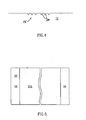
- Fig. 4 shows a cross-sectional view of a photoreceptor 12 in which a roughened portion 26' is generated by forming grooves 28 in the photoreceptor. These grooves may be formed by etching, laser scribing, grooving with a knife or scratching the photoreceptor or by not coating support layer 152 with the upper layers. While triangular grooves are shown, other groove shapes, such as rectangular can be used.
- the level of scratching is highest when the backing layer is not exposed, much lower when the photoconductive and conducting layers are removed chemically and even lower when these layers are not formed at all over the backing layer.
- scratching may not be completely removed by any of these measures.
- Applicants have found that increasing the depth of the grooves up to 50 micrometers in depth and width is effective to further decrease the amount of scratching. While there does not appear to be a threshold for the effect, significant improvement is found with grooving that is 20 micrometers deep. The depth of the grooves is limited by the present thickness of the base layer (experimental grooving has been performed on bare backing layers), namely 70 micrometers. It is believed that deeper grooves and or grooves with larger internal areas (such as square or rectangular grooves) may provide better capture and release of the particles.
- the grooves may be formed by drawing a shaped tool over the surface, by laser milling, by chemical etching or by other means known in the art.
- the surfaces may be roughened by abrasive action of a powder or a solid block or by the action of a chemical such as a Phenol, Nitrobenzene.
- Fig. 5 shows a top view of a sheet photoreceptor formed with roughened portion 26'.
- the roughened portion is a strip with its long dimension in the direction of the drum axis (when mounted).
- This angling also helps to reduce wear on the scrapper, which is generally of a polymer such as polyurethane having a Shore A hardness of between 50 and 80.
- the rough portion is situated near edge 18.
- any intrinsic effect of the roughness on the quality of images formed on the photoreceptor will not effect the images actually formed, since this portion is not used in forming the images.
- the photoreceptor blanket, drum or belt
- the paper feed must be synchronously operated so that the seam is not positioned in the image.
Landscapes
- Physics & Mathematics (AREA)
- General Physics & Mathematics (AREA)
- Photoreceptors In Electrophotography (AREA)
- Discharging, Photosensitive Material Shape In Electrophotography (AREA)
Applications Claiming Priority (1)
| Application Number | Priority Date | Filing Date | Title |
|---|---|---|---|
| PCT/IL2001/000818 WO2003019296A1 (en) | 2001-08-30 | 2001-08-30 | Scratch resistant organic photoreceptor |
Publications (2)
| Publication Number | Publication Date |
|---|---|
| EP1446704A1 EP1446704A1 (en) | 2004-08-18 |
| EP1446704B1 true EP1446704B1 (en) | 2009-11-11 |
Family
ID=11043088
Family Applications (1)
| Application Number | Title | Priority Date | Filing Date |
|---|---|---|---|
| EP01963356A Expired - Lifetime EP1446704B1 (en) | 2001-08-30 | 2001-08-30 | Scratch resistant organic photoreceptor |
Country Status (6)
| Country | Link |
|---|---|
| US (1) | US20040197689A1 (enExample) |
| EP (1) | EP1446704B1 (enExample) |
| JP (1) | JP3939696B2 (enExample) |
| CA (1) | CA2459102A1 (enExample) |
| DE (1) | DE60140490D1 (enExample) |
| WO (1) | WO2003019296A1 (enExample) |
Families Citing this family (4)
| Publication number | Priority date | Publication date | Assignee | Title |
|---|---|---|---|---|
| WO2005093519A1 (ja) * | 2004-03-26 | 2005-10-06 | Canon Kabushiki Kaisha | 電子写真感光体、電子写真感光体の製造方法、プロセスカートリッジおよび電子写真装置 |
| JP5549917B2 (ja) * | 2008-11-07 | 2014-07-16 | 株式会社リコー | 電子写真感光体、それを用いた画像形成方法、画像形成装置及び画像形成装置用プロセスカートリッジ |
| WO2011067853A1 (ja) * | 2009-12-04 | 2011-06-09 | キヤノン株式会社 | 電子写真感光体、プロセスカートリッジおよび電子写真装置 |
| US9031470B2 (en) * | 2012-06-07 | 2015-05-12 | Hewlett-Packard Indigo B.V. | LEP printer, a photo imaging plate for such printer and a method for wiping such photo imaging plate |
Family Cites Families (18)
| Publication number | Priority date | Publication date | Assignee | Title |
|---|---|---|---|---|
| US3994726A (en) * | 1974-04-25 | 1976-11-30 | Xerox Corporation | Method of forming a resilient photoconductive element |
| US4002476A (en) * | 1975-05-23 | 1977-01-11 | Xerox Corporation | Method of developing resilient photoconductive element |
| US4002726A (en) * | 1975-07-16 | 1977-01-11 | The United States Of America As Represented By The United States Energy Research And Development Administration | Method of recycling lithium borate to lithium borohydride through methyl borate |
| JPS59136737A (ja) * | 1983-01-25 | 1984-08-06 | Fuji Electric Co Ltd | 電子写真用感光体 |
| US5148639A (en) * | 1988-07-29 | 1992-09-22 | Canon Kabushiki Kaisha | Surface roughening method for organic electrophotographic photosensitive member |
| JP2702252B2 (ja) * | 1989-12-19 | 1998-01-21 | キヤノン株式会社 | 有機電子写真感光体の表面粗面化法 |
| EP0690350B1 (en) * | 1990-05-08 | 2007-01-24 | Hewlett-Packard Indigo B.V. | Organic photoconductor |
| US5187039A (en) * | 1990-07-31 | 1993-02-16 | Xerox Corporation | Imaging member having roughened surface |
| JPH04120551A (ja) * | 1990-09-12 | 1992-04-21 | Canon Inc | 電子写真感光体 |
| US5242776A (en) * | 1990-11-08 | 1993-09-07 | Minolta Camera Kabushiki Kaisha | Organic photosensitive member having fine irregularities on its surface |
| JPH04369654A (ja) * | 1991-06-19 | 1992-12-22 | Fuji Electric Co Ltd | 電子写真用感光体の製造方法 |
| JP2882210B2 (ja) * | 1992-11-05 | 1999-04-12 | シャープ株式会社 | 電子写真感光体、該感光体の製造方法および該感光体を用いた画像補正方法 |
| US5381211A (en) * | 1993-05-24 | 1995-01-10 | Xerox Corporation | Texturing of overcoated imaging member for cleaning |
| JPH0876642A (ja) * | 1994-09-02 | 1996-03-22 | Ricoh Co Ltd | 潜像担持体および該潜像担持体を用いた画像形成装置 |
| CA2199374A1 (en) * | 1994-09-07 | 1996-03-14 | Haim Belinkov | Imaging apparatus and photoreceptor therefor |
| IL117950A (en) * | 1996-04-17 | 2004-09-27 | Hewlett Packard Indigo Bv | Imaging apparatus and photoreceptor therefor |
| JP3250962B2 (ja) * | 1996-09-13 | 2002-01-28 | 京セラ株式会社 | 感光体および画像形成装置 |
| US5965243A (en) * | 1997-04-04 | 1999-10-12 | 3M Innovative Properties Company | Electrostatic receptors having release layers with texture and means for providing such receptors |
-
2001
- 2001-08-30 US US10/487,744 patent/US20040197689A1/en not_active Abandoned
- 2001-08-30 WO PCT/IL2001/000818 patent/WO2003019296A1/en not_active Ceased
- 2001-08-30 EP EP01963356A patent/EP1446704B1/en not_active Expired - Lifetime
- 2001-08-30 JP JP2003523296A patent/JP3939696B2/ja not_active Expired - Fee Related
- 2001-08-30 DE DE60140490T patent/DE60140490D1/de not_active Expired - Lifetime
- 2001-08-30 CA CA002459102A patent/CA2459102A1/en not_active Abandoned
Also Published As
| Publication number | Publication date |
|---|---|
| WO2003019296A1 (en) | 2003-03-06 |
| JP2005501281A (ja) | 2005-01-13 |
| CA2459102A1 (en) | 2003-03-06 |
| DE60140490D1 (de) | 2009-12-24 |
| JP3939696B2 (ja) | 2007-07-04 |
| US20040197689A1 (en) | 2004-10-07 |
| EP1446704A1 (en) | 2004-08-18 |
Similar Documents
| Publication | Publication Date | Title |
|---|---|---|
| CN106133611B (zh) | 电子照相感光体和具备该电子照相感光体的图像形成装置 | |
| KR20080013810A (ko) | 화상 가열 장치 | |
| CN101046655A (zh) | 具有带有不同组分的多个磁刷辊子的静电记录显影剂单元 | |
| JP2749674B2 (ja) | 潤滑剤含浸金属清掃ブレードおよび製法 | |
| JPH07104636B2 (ja) | 定着装置 | |
| EP0708385A3 (en) | Image forming apparatus | |
| US8965264B2 (en) | Blade member, cleaner and image forming apparatus | |
| EP1446704B1 (en) | Scratch resistant organic photoreceptor | |
| US20020031648A1 (en) | Peeling member | |
| US5381211A (en) | Texturing of overcoated imaging member for cleaning | |
| KR102742527B1 (ko) | 현상제 담지체, 현상 장치, 프로세스 카트리지 및 화상 형성 장치 | |
| EP0528556A2 (en) | Cleaning device | |
| EP1818731A1 (en) | Developing Device, Process Cartridge and Image Forming Apparatus | |
| US11036161B2 (en) | Developer bearing member, developing apparatus, process cartridge, and image forming apparatus | |
| JPS6410073B2 (enExample) | ||
| EP1111477B1 (en) | Toner fixing apparatus with a heat roller pressed by first and second pressing rollers | |
| US8177604B2 (en) | Surface abrading method of photosensitive layer of electrophotographic photoreceptor | |
| US5040030A (en) | Precise loading blade and method for making same | |
| JP2841639B2 (ja) | 画像形成装置の用紙剥離装置 | |
| US20110070537A1 (en) | Electrophotographic photoreceptor | |
| JP2749882B2 (ja) | 電子写真感光体の表面粗面化処理方法 | |
| JP2009276440A (ja) | 電子写真感光体の研磨方法 | |
| JPS5824178A (ja) | ブレ−ドクリ−ニング装置 | |
| JP2002072800A (ja) | クリーニング装置及びこれを用いた画像形成装置 | |
| US6697599B2 (en) | Device for removing a coating adhering to an intermediate carrier in an electrophotographic printer or copier device |
Legal Events
| Date | Code | Title | Description |
|---|---|---|---|
| PUAI | Public reference made under article 153(3) epc to a published international application that has entered the european phase |
Free format text: ORIGINAL CODE: 0009012 |
|
| 17P | Request for examination filed |
Effective date: 20040315 |
|
| AK | Designated contracting states |
Kind code of ref document: A1 Designated state(s): AT BE CH CY DE DK ES FI FR GB GR IE IT LI LU MC NL PT SE TR |
|
| AX | Request for extension of the european patent |
Extension state: AL LT LV MK RO SI |
|
| 17Q | First examination report despatched |
Effective date: 20070404 |
|
| GRAP | Despatch of communication of intention to grant a patent |
Free format text: ORIGINAL CODE: EPIDOSNIGR1 |
|
| GRAS | Grant fee paid |
Free format text: ORIGINAL CODE: EPIDOSNIGR3 |
|
| GRAA | (expected) grant |
Free format text: ORIGINAL CODE: 0009210 |
|
| AK | Designated contracting states |
Kind code of ref document: B1 Designated state(s): DE FR GB IT |
|
| REG | Reference to a national code |
Ref country code: GB Ref legal event code: FG4D |
|
| REF | Corresponds to: |
Ref document number: 60140490 Country of ref document: DE Date of ref document: 20091224 Kind code of ref document: P |
|
| PLBE | No opposition filed within time limit |
Free format text: ORIGINAL CODE: 0009261 |
|
| STAA | Information on the status of an ep patent application or granted ep patent |
Free format text: STATUS: NO OPPOSITION FILED WITHIN TIME LIMIT |
|
| 26N | No opposition filed |
Effective date: 20100812 |
|
| REG | Reference to a national code |
Ref country code: FR Ref legal event code: PLFP Year of fee payment: 16 |
|
| REG | Reference to a national code |
Ref country code: FR Ref legal event code: PLFP Year of fee payment: 17 |
|
| PGFP | Annual fee paid to national office [announced via postgrant information from national office to epo] |
Ref country code: DE Payment date: 20170719 Year of fee payment: 17 Ref country code: GB Payment date: 20170719 Year of fee payment: 17 Ref country code: IT Payment date: 20170719 Year of fee payment: 17 Ref country code: FR Payment date: 20170720 Year of fee payment: 17 |
|
| REG | Reference to a national code |
Ref country code: DE Ref legal event code: R119 Ref document number: 60140490 Country of ref document: DE |
|
| GBPC | Gb: european patent ceased through non-payment of renewal fee |
Effective date: 20180830 |
|
| PG25 | Lapsed in a contracting state [announced via postgrant information from national office to epo] |
Ref country code: DE Free format text: LAPSE BECAUSE OF NON-PAYMENT OF DUE FEES Effective date: 20190301 Ref country code: IT Free format text: LAPSE BECAUSE OF NON-PAYMENT OF DUE FEES Effective date: 20180830 |
|
| PG25 | Lapsed in a contracting state [announced via postgrant information from national office to epo] |
Ref country code: FR Free format text: LAPSE BECAUSE OF NON-PAYMENT OF DUE FEES Effective date: 20180831 |
|
| PG25 | Lapsed in a contracting state [announced via postgrant information from national office to epo] |
Ref country code: GB Free format text: LAPSE BECAUSE OF NON-PAYMENT OF DUE FEES Effective date: 20180830 |