EP1443754A2 - Camera module and manufacturing method thereof - Google Patents
Camera module and manufacturing method thereof Download PDFInfo
- Publication number
- EP1443754A2 EP1443754A2 EP04001675A EP04001675A EP1443754A2 EP 1443754 A2 EP1443754 A2 EP 1443754A2 EP 04001675 A EP04001675 A EP 04001675A EP 04001675 A EP04001675 A EP 04001675A EP 1443754 A2 EP1443754 A2 EP 1443754A2
- Authority
- EP
- European Patent Office
- Prior art keywords
- lens
- image sensor
- camera module
- lens frame
- array
- Prior art date
- Legal status (The legal status is an assumption and is not a legal conclusion. Google has not performed a legal analysis and makes no representation as to the accuracy of the status listed.)
- Withdrawn
Links
Images


Classifications
-
- H—ELECTRICITY
- H04—ELECTRIC COMMUNICATION TECHNIQUE
- H04N—PICTORIAL COMMUNICATION, e.g. TELEVISION
- H04N23/00—Cameras or camera modules comprising electronic image sensors; Control thereof
- H04N23/50—Constructional details
- H04N23/55—Optical parts specially adapted for electronic image sensors; Mounting thereof
-
- G—PHYSICS
- G01—MEASURING; TESTING
- G01B—MEASURING LENGTH, THICKNESS OR SIMILAR LINEAR DIMENSIONS; MEASURING ANGLES; MEASURING AREAS; MEASURING IRREGULARITIES OF SURFACES OR CONTOURS
- G01B11/00—Measuring arrangements characterised by the use of optical techniques
- G01B11/16—Measuring arrangements characterised by the use of optical techniques for measuring the deformation in a solid, e.g. optical strain gauge
-
- G—PHYSICS
- G01—MEASURING; TESTING
- G01M—TESTING STATIC OR DYNAMIC BALANCE OF MACHINES OR STRUCTURES; TESTING OF STRUCTURES OR APPARATUS, NOT OTHERWISE PROVIDED FOR
- G01M11/00—Testing of optical apparatus; Testing structures by optical methods not otherwise provided for
- G01M11/08—Testing mechanical properties
- G01M11/088—Testing mechanical properties of optical fibres; Mechanical features associated with the optical testing of optical fibres
Definitions
- This invention relates to a camera module and its manufacturing method, specifically to a small size camera module suitable to be incorporated into a portable device such as a mobile phone and a manufacturing method of it.
- FIG. 15 is a cross-sectional view showing a structure of such a camera module.
- Fig. 15 shows a lens-barrel 50, a lens 51 mounted inside the lens-barrel 50 and an IR filter 52 to block infrared radiation attached to a mouth of the lens-barrel 50. It also shows an image sensor chip 60 housed in a space within the lens-barrel 50 and electrically connected with a printed circuit board 70.
- the image sensor chip 60 converts light incident on it from a photogenic subject through the IR filter 52 and the lens 51 into electric signals.
- CCDs Charge Coupled Devices
- a supporting glass substrate 62 is bonded to the silicon chip 61 to bolster it.
- Each of redistribution wirings 64A and 64B is formed extending from each of electrode pads 63A and 63B, which are formed on a peripheral surface of the image sensor chip 60, over a side surface and to a back surface of the silicon chip 61.
- Each of the redistribution wirings 64A and 64B extends onto a glass substrate 65 which is bonded to the back surface of the silicon chip 61.
- Each of bump electrodes 66A and 66B is formed on an end of each of the redistribution wirings 64A and 64B extended onto the glass substrate 65.
- the bump electrodes 66A and 66B are connected to the printed circuit board 70.
- a DSP (Digital Signal Processor) 80 which performs video signal processing on the electric signals from the image sensor chip 60, is connected to a back surface of the printed circuit board 70 through bump electrodes 81A and 81B.
- the lens-barrel 50, the lens 51, the IR filter 52 and the image sensor chip 60 are discrete components, and the camera module is assembled by putting these discrete components together. This causes difficulty in reducing the size and manufacturing cost of the camera module.
- the invention provides a camera module that includes an image sensor unit having an image sensor chip that has a photoelectronic transducer disposed in its top surface and a terminal for external connection disposed on its back surface, a first lens bonded to the top surface of the image sensor unit, and a second lens bonded onto the first lens.
- the invention also provides a manufacturing method of a camera module.
- the method includes providing an image sensor wafer having a plurality of image sensor chips. Each of the image sensor chips has a photoelectronic transducer disposed in the top surface thereof and a terminal for external connection disposed on the back surface thereof.
- the method also includes providing a first lens array having a plurality of first lenses and a second lens array having a plurality of second lenses, bonding the image sensor wafer, the first lens array and the second lens array to form a bonded unit, and dividing the bonded unit into individual camera modules so that each of the camera modules includes one of the image sensor chips, one of the first lenses and one of the second lenses.
- camera modules having a compound lens are provided that allow for an increased picture quality combined with a cost effective manufacturing.
- Fig. 1 is a plan view showing the camera module
- Fig. 2 is a cross-sectional view showing a section X-X in Fig. 1.
- Basic structure of the camera module is an integrated unit composed of an image sensor chip 20, a first lens 10 bonded onto the image sensor chip 20 and a second lens 30 bonded to the first lens 20 so that the two lenses face to each other.
- an iris material 40 made of a film such as an acrylic film or a polyolefin film is bonded to the second lens 30.
- an IR filter 45 is bonded between the image sensor chip 20 and the first lens 10.
- the first lens 10 is composed of a first lens body 11 which is circular-shaped on the plan view and a first lens frame 12 provided around the first lens body 11 to bolster it and molded together with the first lens body 11.
- the second lens 30 is composed of a second lens body 31 which is circular-shaped on the plan view and a second lens frame 32 provided around the second lens body 31 to bolster it and molded together with the second lens body 31.
- a surface of the first lens frame 12 is bonded to a peripheral surface of the image sensor chip 20 through the IR filter 45 using an adhesive.
- the other surface of the first lens frame 12 is bonded to the second lens frame 32 using an adhesive.
- the first lens body 11 and the second lens body 31 have predetermined shape of curved surface in order to obtain desired optical characteristics. Heights of the first lens frame 12 and the second lens frame 32 are determined to place centers (indicated by alternate long and short dashed lines in Fig. 2) of the first lens body 11 and the second lens body 32 at predetermined distances h1 and h2 from the surface of the image sensor chip 20, respectively.
- CCDs which are photoelectronic transducers, are formed in a surface of a silicon chip 21, and a supporting glass substrate 22 is bonded to the silicon chip 21 using an adhesive or the like to bolster the silicon chip 21 which is as thin as several hundred micrometers.
- Electrode pads 23A and 23B are formed on a peripheral surface of the silicon chip 21. Each of the electrode pads 23A and 23B is connected with an input/output circuit of the image sensor chip 20.
- each of the electrode pads 23A and 23B is connected with each of redistribution wirings 24A and 24B which penetrate through the silicon chip 21 to reach a back surface of the image sensor chip 20.
- Each of bump electrodes 25A and 25B which serve as terminals for external connection, is formed on an exposed surface of each of the redistribution wirings 24A and 24B.
- the IR filter 45 is bonded between the image sensor chip 20 and the first lens 10 in the structure described above, the IR filter may be bonded onto the second lens frame 32 of the second lens 30. In this case, the iris material 40 is formed on the IR filter 45. And the first lens 10 is bonded onto the image sensor chip 20 directly.
- the IR filter 45 can be omitted, leading to cost reduction due to reduction in number of parts.
- the filtering function is obtained by vacuum deposition of metal on the supporting glass substrate 22 or incorporating copper particles into the supporting glass substrate 22.
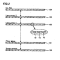
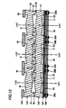
- An image sensor wafer 100 in which a plurality of image sensor chips 20 formed by wafer processing is disposed in a matrix form, is provided as shown in Fig. 3. And an IR filter glass 101 in the same shape as the wafer is provided. Also, a first lens array 102, which is formed by integrating a plurality of the first lenses 10 each having equivalent shape and size to the image sensor chip 20, is provided. Also, a second lens array 103, which is formed by integrating a plurality of the second lenses 30 each having equivalent shape and size to the image sensor chip 20, is provided. An iris film 104 having a shape of the wafer is also provided.
- the image sensor wafer 100, the IR filter glass 101, the first lens array 102, the second lens array 103 and the iris film 104 are bonded together, forming an integrated structure.
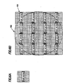
- Fig. 4A is a plan view showing a first example of the first lens array 102.
- the first example of the first lens array 102 has a multitude of the first lenses 10 arranged to make an envelope of the array in a shape essentially same as the wafer, as shown in Fig. 4A.
- the first lens array 102 is bonded onto the image sensor wafer 100, as shown in Fig. 4B.
- Fig. 5A is a plan view showing a second example of the first lens array 102.
- the second example of the first lens array 102 is composed of two kinds of sub-arrays, i.e., sub-arrays A and sub-arrays B, each of the sub-arrays being nearly triangular shaped, as shown in Fig. 5A.
- Four each of the sub-array A and the sub-array B are bonded to the image sensor wafer 100, as shown in Fig. 5B.
- Fig. 6A is a plan view showing a third example of the first lens array 102.
- the third example of the first lens array 102 is composed of a single kind of rectangular sub-arrays, as shown in Fig. 6A.
- the third example of the first lens array 102 has an advantage of manufacturing simplicity, since it is composed of a single kind of sub-arrays.
- the second lens array 103 is formed in the same way as the first lens array 102.
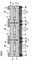
- Fig. 7 is a cross-sectional view of the integrated structure formed by bonding the image sensor wafer 100, the IR filter glass 101, the first lens array 102, the second lens array 103 and the iris film 104 together.
- the first lens frame 12 of the first lens array 102 is disposed across a border between two neighboring image sensor chips 20, in a way that a center line of the first lens frame 12 approximately coincides with the border, as shown in the figure.
- the second lens frame 32 of the second lens array 103 is bonded to a top surface of the first lens frame 12.
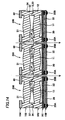
- the integrated structure described above is divided into individual camera modules 200 by cutting along borders between the image sensor chips 20 with a dicing blade or a laser, as shown in Fig. 8.
- the first lens frame 12 and the second lens frame 32 are divided into approximately half in width at the same time.
- each of the individual camera modules 200 is mounted on a printed circuit board through bump electrodes 25A and 25B on the back surface of the image sensor chip 20.
- first lens 10 and the second lens 30 are made of plastic, heat resistance of the plastic comes into question, because heat treatment is applied on the bump electrodes 25A and 25B usually when the camera module 200 is mounted on the printed circuit board. In this case, it is better to use a plastic material with a higher heat resistance or gold bumps which can be connected at lower temperature.
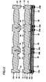
- a first lens 10 and a second lens 30 are bonded with an adhesive at a first lens frame 12 and a second lens frame 32 respectively, as described in the first embodiment.
- concave portions 13 for guide in the first lens frames 12 and convex portions 33 for guide in the second lens frames 32 are formed in advance, so that when bonding the first lens array 102 to the second lens array 103 the concave portions 13 for guide fit with the convex portions 33 for guide to prevent the misalignment in direction parallel to the bonding plane (horizontal direction in Fig. 7), as shown in Fig. 9. Alignment between the optical axis LA1 of the first lens body 11 and the optical axis LA2 of the second lens body 31 is thereby made easier than in the first embodiment.
- the convex portions for guide may be formed in the first lens frame 12 while the concave portions for guide are formed in the second lens frame 32 on the contrary to above description.
- the second lens array 103 is bonded to the first lens array 102 and an iris film 104 is bonded to the second lens array 103 as shown in Fig. 10, forming an integrated structure.
- the integrated structure described above is divided into individual camera modules 200 by cutting along borders between image sensor chips 20 with a dicing blade or a laser, as shown in Fig. 11.
- ditches 34 to absorb the error in dimension are formed in the bonding surfaces of the second lens frames 32, as shown in Fig. 12. Depth of the ditches 34 is less than thickness of the second lens frame 32.
- the ditches may be formed by cutting the second lens frames 32 with a dicing apparatus.
- each of the concave portions 13 for guide fits exactly with each of the convex portions 33 for guide. As a result, it becomes easy to make the optical axis LA1 of the first lens body 11 coincide with the optical axis LA2 of the second lens body 31 in all of the camera modules 200.
- the second lens array 103 is bonded to the first lens array 102 and an iris film 104 is bonded to the second lens array 103 as shown in Fig. 13, forming an integrated structure.
- the integrated structure described above is divided into individual camera modules 200 by cutting along borders between image sensor chips 20 with a dicing blade or a laser, as shown in Fig. 14.
- the camera module for a portable device is miniaturized to a size of the image sensor chip as well as its manufacturing cost is substantially reduced according to this invention.
- the camera module is capable of high quality picture of 300,000 pixels or above, since it has a compound lens.
Applications Claiming Priority (2)
| Application Number | Priority Date | Filing Date | Title |
|---|---|---|---|
| JP2003017012 | 2003-01-27 | ||
| JP2003017012A JP2004226872A (ja) | 2003-01-27 | 2003-01-27 | カメラモジュール及びその製造方法 |
Publications (1)
| Publication Number | Publication Date |
|---|---|
| EP1443754A2 true EP1443754A2 (en) | 2004-08-04 |
Family
ID=32652826
Family Applications (1)
| Application Number | Title | Priority Date | Filing Date |
|---|---|---|---|
| EP04001675A Withdrawn EP1443754A2 (en) | 2003-01-27 | 2004-01-27 | Camera module and manufacturing method thereof |
Country Status (6)
| Country | Link |
|---|---|
| US (1) | US20040212719A1 (ja) |
| EP (1) | EP1443754A2 (ja) |
| JP (1) | JP2004226872A (ja) |
| KR (1) | KR20040068865A (ja) |
| CN (1) | CN1517736A (ja) |
| TW (1) | TW200421863A (ja) |
Cited By (14)
| Publication number | Priority date | Publication date | Assignee | Title |
|---|---|---|---|---|
| FR2936098A1 (fr) * | 2008-08-25 | 2010-03-19 | Cheng Uei Prec Ind Co Ltd | Module de camera et procede de fabrication |
| EP2259096A1 (en) * | 2009-06-03 | 2010-12-08 | Samsung Electronics Co., Ltd. | Wafer-level lens module and image pickup module including the same |
| US8120858B2 (en) | 2008-12-04 | 2012-02-21 | Samsung Electronics Co., Ltd. | Micro lens, method and apparatus for manufacturing micro lens, and camera module including micro lens |
| US8305699B2 (en) | 2009-09-23 | 2012-11-06 | Samsung Electronics Co., Ltd. | Wafer-level lens module with extended depth of field and imaging device including the wafer-level lens module |
| US8456560B2 (en) | 2007-01-26 | 2013-06-04 | Digitaloptics Corporation | Wafer level camera module and method of manufacture |
| US8475061B2 (en) | 2008-01-16 | 2013-07-02 | Omnivision Technologies, Inc. | Membrane suspended optical elements, and associated methods |
| US8520137B2 (en) | 2009-08-13 | 2013-08-27 | Samsung Electronics Co., Ltd. | Wafer-level lens module and image pickup device including the same |
| US8605208B2 (en) | 2007-04-24 | 2013-12-10 | Digitaloptics Corporation | Small form factor modules using wafer level optics with bottom cavity and flip-chip assembly |
| US8885272B2 (en) | 2011-05-03 | 2014-11-11 | Omnivision Technologies, Inc. | Flexible membrane and lens assembly and associated method of lens replication |
| US9419032B2 (en) | 2009-08-14 | 2016-08-16 | Nanchang O-Film Optoelectronics Technology Ltd | Wafer level camera module with molded housing and method of manufacturing |
| EP2298543A3 (en) * | 2009-09-17 | 2016-09-07 | FUJIFILM Corporation | Master model of lens array and method of manufacturing the same |
| EP2298544A3 (en) * | 2009-09-16 | 2016-10-05 | FUJIFILM Corporation | Wafer-level lens array, method of manufacturing wafer-level lens array, lens module and imaging unit |
| DE102015226173A1 (de) * | 2015-12-21 | 2017-06-22 | Robert Bosch Gmbh | Optisches Abbildungssystem mit einer aufgrund elektrischer und/oder magnetischer Kräfte verformbaren Linse |
| WO2019044540A1 (en) * | 2017-08-31 | 2019-03-07 | Sony Semiconductor Solutions Corporation | IMAGING APPARATUS AND ELECTRONIC APPARATUS |
Families Citing this family (51)
| Publication number | Priority date | Publication date | Assignee | Title |
|---|---|---|---|---|
| KR100547745B1 (ko) * | 2003-10-23 | 2006-01-31 | 삼성전자주식회사 | 카메라 장치의 이미지 센서 모듈 및 그 조립방법 |
| KR100649490B1 (ko) * | 2004-06-14 | 2006-11-24 | 삼성전기주식회사 | 카메라폰용 카메라모듈 |
| JP4349232B2 (ja) * | 2004-07-30 | 2009-10-21 | ソニー株式会社 | 半導体モジュール及びmos型固体撮像装置 |
| JP4379295B2 (ja) | 2004-10-26 | 2009-12-09 | ソニー株式会社 | 半導体イメージセンサー・モジュール及びその製造方法 |
| KR100691184B1 (ko) * | 2005-06-28 | 2007-03-09 | 삼성전기주식회사 | 웨이퍼 스케일 렌즈의 적층을 위한 접착방법 및 이에 의해제조된 웨이퍼 스케일 렌즈 |
| JP4585409B2 (ja) * | 2005-08-24 | 2010-11-24 | 株式会社東芝 | 小型カメラモジュール |
| KR100652551B1 (ko) | 2005-11-07 | 2006-12-01 | 삼성전기주식회사 | 소형 카메라 모듈 및 그 제조방법 |
| KR100744925B1 (ko) * | 2005-12-27 | 2007-08-01 | 삼성전기주식회사 | 카메라 모듈 패키지 |
| CN100405107C (zh) * | 2006-01-06 | 2008-07-23 | 林颖诚 | 手机照相模块滤光片及其制造方法 |
| JP2007221231A (ja) * | 2006-02-14 | 2007-08-30 | Denso Corp | 撮像モジュールおよびその製造方法 |
| KR101210039B1 (ko) * | 2006-03-13 | 2012-12-07 | 엘지이노텍 주식회사 | 카메라 모듈 |
| US20070236591A1 (en) * | 2006-04-11 | 2007-10-11 | Tam Samuel W | Method for mounting protective covers over image capture devices and devices manufactured thereby |
| EP2069851A4 (en) * | 2006-09-14 | 2010-02-24 | Tessera Tech Hungary Kft | IMAGING SYSTEM WITH ASSOUPLY ASSEMBLED TOLERANCES AND ASSOCIATED METHODS |
| WO2008087486A2 (en) * | 2006-09-14 | 2008-07-24 | Tessera Technologies Hungary Kft. | Imaging system with improved image quality and associated methods |
| US20090015706A1 (en) * | 2007-04-24 | 2009-01-15 | Harpuneet Singh | Auto focus/zoom modules using wafer level optics |
| US7825985B2 (en) * | 2007-07-19 | 2010-11-02 | Flextronics Ap, Llc | Camera module back-focal length adjustment method and ultra compact components packaging |
| JP5026198B2 (ja) * | 2007-08-28 | 2012-09-12 | 日立マクセル株式会社 | レンズユニット、レンズモジュール、カメラモジュール及びカメラモジュール搭載回路基板の製造方法 |
| JP4799543B2 (ja) * | 2007-12-27 | 2011-10-26 | 株式会社東芝 | 半導体パッケージ及びカメラモジュール |
| US9118825B2 (en) | 2008-02-22 | 2015-08-25 | Nan Chang O-Film Optoelectronics Technology Ltd. | Attachment of wafer level optics |
| JP4966931B2 (ja) | 2008-08-26 | 2012-07-04 | シャープ株式会社 | 電子素子ウエハモジュールおよびその製造方法、電子素子モジュールおよびその製造方法、電子情報機器 |
| JP4764941B2 (ja) * | 2008-09-25 | 2011-09-07 | シャープ株式会社 | 光学素子、光学素子ウエハ、光学素子ウエハモジュール、光学素子モジュール、光学素子モジュールの製造方法、電子素子ウエハモジュール、電子素子モジュールの製造方法、電子素子モジュールおよび電子情報機器 |
| WO2010038554A1 (ja) * | 2008-09-30 | 2010-04-08 | コニカミノルタオプト株式会社 | 光学部品の製造方法並びにレンズ、レンズユニット及びカメラモジュール |
| JP4832500B2 (ja) * | 2008-12-01 | 2011-12-07 | シャープ株式会社 | 電子素子ウエハモジュールの製造方法および光学素子ウエハモジュールの製造方法 |
| JP5254139B2 (ja) * | 2009-07-03 | 2013-08-07 | シャープ株式会社 | 多層レンズ、積層型ウェハレンズおよびその製造方法 |
| JP5345455B2 (ja) * | 2009-07-03 | 2013-11-20 | シャープ株式会社 | 多層レンズ、積層型ウェハレンズおよびその製造方法 |
| JP5450633B2 (ja) * | 2009-09-09 | 2014-03-26 | 株式会社東芝 | 固体撮像装置およびその製造方法 |
| JP5448685B2 (ja) * | 2009-09-30 | 2014-03-19 | 富士フイルム株式会社 | 素子アレイ、素子アレイ積層体、及び素子アレイ積層体の製造方法 |
| JP5572355B2 (ja) * | 2009-09-30 | 2014-08-13 | 富士フイルム株式会社 | レンズアレイ及びレンズアレイ積層体 |
| CN102045494A (zh) * | 2009-10-22 | 2011-05-04 | 国碁电子(中山)有限公司 | 相机模组及其制作方法 |
| JP4819204B2 (ja) * | 2009-10-28 | 2011-11-24 | パナソニック株式会社 | レンズシート、表示パネル装置、および表示装置 |
| TWM382505U (en) * | 2010-01-15 | 2010-06-11 | Cheng Uei Prec Ind Co Ltd | Video device |
| EP2369371A3 (en) * | 2010-03-10 | 2013-05-01 | Fujifilm Corporation | Wafer lens array and method for manufacturing the same |
| JP2011209699A (ja) * | 2010-03-10 | 2011-10-20 | Fujifilm Corp | ウェハレンズアレイ及びその製造方法 |
| US9910239B2 (en) * | 2010-11-30 | 2018-03-06 | Flir Systems Trading Belgium Bvba | Wafer level optical elements and applications thereof |
| CN103314313B (zh) * | 2011-01-21 | 2014-08-06 | 富士胶片株式会社 | 堆叠型透镜阵列、透镜模块及摄像单元 |
| US10009528B2 (en) | 2011-02-24 | 2018-06-26 | Nan Chang O-Film Optoelectronics Technology Ltd | Autofocus camera module packaging with circuitry-integrated actuator system |
| US8545114B2 (en) | 2011-03-11 | 2013-10-01 | Digitaloptics Corporation | Auto focus-zoom actuator or camera module contamination reduction feature with integrated protective membrane |
| TWI461742B (zh) * | 2012-01-09 | 2014-11-21 | Largan Precision Co Ltd | 複層陣列鏡片組 |
| CN102903726B (zh) * | 2012-09-29 | 2016-02-10 | 格科微电子(上海)有限公司 | 图像传感器的晶圆级封装方法 |
| CN104937447A (zh) * | 2012-12-28 | 2015-09-23 | 尤米科尔公司 | 用于ir光学系统的前孔径光阑 |
| US9923008B2 (en) | 2013-04-12 | 2018-03-20 | Omnivision Technologies, Inc. | Wafer-level array cameras and methods for fabricating the same |
| US9088705B1 (en) | 2013-08-30 | 2015-07-21 | Amazon Technologies, Inc. | Camera module package with stiffener-mounted image sensor die |
| US9241097B1 (en) | 2013-09-27 | 2016-01-19 | Amazon Technologies, Inc. | Camera module including image sensor die in molded cavity substrate |
| WO2015099209A1 (ko) * | 2013-12-23 | 2015-07-02 | 엘지전자 주식회사 | 카메라 모듈 |
| JP6967830B2 (ja) * | 2015-07-31 | 2021-11-17 | ソニーセミコンダクタソリューションズ株式会社 | 半導体装置、レンズモジュール及びその製造方法、並びに、電子機器 |
| US10488632B2 (en) * | 2016-01-20 | 2019-11-26 | Mems Optical Zoom Corporation | MEMS lens actuator |
| US10466501B2 (en) * | 2016-05-26 | 2019-11-05 | Ams Sensors Singapore Pte. Ltd. | Optoelectronic modules including an optical system tilted with respect to a focal plane |
| US10925160B1 (en) | 2016-06-28 | 2021-02-16 | Amazon Technologies, Inc. | Electronic device with a display assembly and silicon circuit board substrate |
| JP6976751B2 (ja) * | 2017-07-06 | 2021-12-08 | ソニーセミコンダクタソリューションズ株式会社 | 撮像装置および撮像装置の製造方法、並びに、電子機器 |
| CN112217964A (zh) * | 2019-07-11 | 2021-01-12 | 南昌欧菲光电技术有限公司 | 支架、摄像模组及电子设备终端 |
| JPWO2021132433A1 (ja) * | 2019-12-25 | 2021-07-01 |
-
2003
- 2003-01-27 JP JP2003017012A patent/JP2004226872A/ja active Pending
- 2003-12-23 TW TW092136482A patent/TW200421863A/zh unknown
-
2004
- 2004-01-20 CN CNA2004100028802A patent/CN1517736A/zh active Pending
- 2004-01-26 KR KR1020040004581A patent/KR20040068865A/ko not_active Application Discontinuation
- 2004-01-27 EP EP04001675A patent/EP1443754A2/en not_active Withdrawn
- 2004-02-05 US US10/771,509 patent/US20040212719A1/en not_active Abandoned
Cited By (17)
| Publication number | Priority date | Publication date | Assignee | Title |
|---|---|---|---|---|
| US8456560B2 (en) | 2007-01-26 | 2013-06-04 | Digitaloptics Corporation | Wafer level camera module and method of manufacture |
| US8605208B2 (en) | 2007-04-24 | 2013-12-10 | Digitaloptics Corporation | Small form factor modules using wafer level optics with bottom cavity and flip-chip assembly |
| EP2240805B1 (en) * | 2008-01-16 | 2014-02-26 | OmniVision CDM Optics, Inc. | Membrane suspended optical elements, and associated methods |
| US8475061B2 (en) | 2008-01-16 | 2013-07-02 | Omnivision Technologies, Inc. | Membrane suspended optical elements, and associated methods |
| DE102008046755A1 (de) * | 2008-08-25 | 2010-03-25 | Cheng Uei Precision Industry Co., Ltd., Tucheng | Kamera-Modul und Verfahren zu seiner Herstellung |
| FR2936098A1 (fr) * | 2008-08-25 | 2010-03-19 | Cheng Uei Prec Ind Co Ltd | Module de camera et procede de fabrication |
| US8120858B2 (en) | 2008-12-04 | 2012-02-21 | Samsung Electronics Co., Ltd. | Micro lens, method and apparatus for manufacturing micro lens, and camera module including micro lens |
| EP2193911A3 (en) * | 2008-12-04 | 2012-05-09 | Samsung Electronics Co., Ltd. | Micro lens, method and apparatus for manufacturing micro lens, and camera module including micro lens |
| EP2259096A1 (en) * | 2009-06-03 | 2010-12-08 | Samsung Electronics Co., Ltd. | Wafer-level lens module and image pickup module including the same |
| US8520137B2 (en) | 2009-08-13 | 2013-08-27 | Samsung Electronics Co., Ltd. | Wafer-level lens module and image pickup device including the same |
| US9419032B2 (en) | 2009-08-14 | 2016-08-16 | Nanchang O-Film Optoelectronics Technology Ltd | Wafer level camera module with molded housing and method of manufacturing |
| EP2298544A3 (en) * | 2009-09-16 | 2016-10-05 | FUJIFILM Corporation | Wafer-level lens array, method of manufacturing wafer-level lens array, lens module and imaging unit |
| EP2298543A3 (en) * | 2009-09-17 | 2016-09-07 | FUJIFILM Corporation | Master model of lens array and method of manufacturing the same |
| US8305699B2 (en) | 2009-09-23 | 2012-11-06 | Samsung Electronics Co., Ltd. | Wafer-level lens module with extended depth of field and imaging device including the wafer-level lens module |
| US8885272B2 (en) | 2011-05-03 | 2014-11-11 | Omnivision Technologies, Inc. | Flexible membrane and lens assembly and associated method of lens replication |
| DE102015226173A1 (de) * | 2015-12-21 | 2017-06-22 | Robert Bosch Gmbh | Optisches Abbildungssystem mit einer aufgrund elektrischer und/oder magnetischer Kräfte verformbaren Linse |
| WO2019044540A1 (en) * | 2017-08-31 | 2019-03-07 | Sony Semiconductor Solutions Corporation | IMAGING APPARATUS AND ELECTRONIC APPARATUS |
Also Published As
| Publication number | Publication date |
|---|---|
| TW200421863A (en) | 2004-10-16 |
| KR20040068865A (ko) | 2004-08-02 |
| US20040212719A1 (en) | 2004-10-28 |
| CN1517736A (zh) | 2004-08-04 |
| JP2004226872A (ja) | 2004-08-12 |
Similar Documents
| Publication | Publication Date | Title |
|---|---|---|
| EP1443754A2 (en) | Camera module and manufacturing method thereof | |
| US20040169763A1 (en) | Camera module and manufacturing method thereof | |
| US6853005B2 (en) | Camera module and manufacturing method thereof | |
| US7166907B2 (en) | Image sensor module with substrate and frame and method of making the same | |
| US7863702B2 (en) | Image sensor package and method of manufacturing the same | |
| KR101442060B1 (ko) | 카메라 모듈 및 촬상장치 | |
| US20070126912A1 (en) | Camera module and manufacturing method for such a camera module | |
| US20060164539A1 (en) | Camera module, camera system and method of manufacturing a camera module | |
| US20150026971A1 (en) | Wafer level camera module and method of manufacture | |
| CN101193204B (zh) | 摄像模块及摄像装置 | |
| JP5035707B2 (ja) | 撮像装置の製造方法及び撮像装置 | |
| US20060109366A1 (en) | Compact lens turret assembly | |
| JP2004229167A (ja) | カメラモジュールの製造方法 | |
| US9111827B2 (en) | Manufacturing method of solid-state imaging apparatus, solid-state imaging apparatus, and electronic imaging apparatus | |
| JP2004233482A (ja) | カメラモジュールの製造方法 | |
| JP4352664B2 (ja) | 半導体装置及びその製造方法 | |
| KR100956381B1 (ko) | 웨이퍼 레벨 카메라 모듈의 제조 방법 | |
| EP1526579A2 (en) | Solid-state imaging device and method for manufacturing the same | |
| KR20100027857A (ko) | 웨이퍼 레벨 카메라 모듈 및 이의 제조방법 | |
| JP2004233483A (ja) | カメラモジュール | |
| EP1713126A1 (en) | Image pickup device and a manufacturing method thereof | |
| JP2003243634A (ja) | 固体撮像装置及びその製造方法 | |
| JPH04172761A (ja) | 密着型リニアイメージセンサモジュール |
Legal Events
| Date | Code | Title | Description |
|---|---|---|---|
| PUAI | Public reference made under article 153(3) epc to a published international application that has entered the european phase |
Free format text: ORIGINAL CODE: 0009012 |
|
| AK | Designated contracting states |
Kind code of ref document: A2 Designated state(s): AT BE BG CH CY CZ DE DK EE ES FI FR GB GR HU IE IT LI LU MC NL PT RO SE SI SK TR |
|
| AX | Request for extension of the european patent |
Extension state: AL LT LV MK |
|
| STAA | Information on the status of an ep patent application or granted ep patent |
Free format text: STATUS: THE APPLICATION IS DEEMED TO BE WITHDRAWN |
|
| 18D | Application deemed to be withdrawn |
Effective date: 20080801 |