EP1443527A1 - SUBSTRATE WITH TRANSPARENT CONDUCTIVE OXIDE FILM AND PRODUCTION METHOD THEREFOR, AND PHOTOELECTRIC CONVERSION ELEMENT - Google Patents
SUBSTRATE WITH TRANSPARENT CONDUCTIVE OXIDE FILM AND PRODUCTION METHOD THEREFOR, AND PHOTOELECTRIC CONVERSION ELEMENT Download PDFInfo
- Publication number
- EP1443527A1 EP1443527A1 EP02775364A EP02775364A EP1443527A1 EP 1443527 A1 EP1443527 A1 EP 1443527A1 EP 02775364 A EP02775364 A EP 02775364A EP 02775364 A EP02775364 A EP 02775364A EP 1443527 A1 EP1443527 A1 EP 1443527A1
- Authority
- EP
- European Patent Office
- Prior art keywords
- substrate
- transparent conductive
- layer
- conductive oxide
- oxide film
- Prior art date
- Legal status (The legal status is an assumption and is not a legal conclusion. Google has not performed a legal analysis and makes no representation as to the accuracy of the status listed.)
- Withdrawn
Links
Images



Classifications
-
- H—ELECTRICITY
- H10—SEMICONDUCTOR DEVICES; ELECTRIC SOLID-STATE DEVICES NOT OTHERWISE PROVIDED FOR
- H10F—INORGANIC SEMICONDUCTOR DEVICES SENSITIVE TO INFRARED RADIATION, LIGHT, ELECTROMAGNETIC RADIATION OF SHORTER WAVELENGTH OR CORPUSCULAR RADIATION
- H10F71/00—Manufacture or treatment of devices covered by this subclass
- H10F71/138—Manufacture of transparent electrodes, e.g. transparent conductive oxides [TCO] or indium tin oxide [ITO] electrodes
-
- C—CHEMISTRY; METALLURGY
- C23—COATING METALLIC MATERIAL; COATING MATERIAL WITH METALLIC MATERIAL; CHEMICAL SURFACE TREATMENT; DIFFUSION TREATMENT OF METALLIC MATERIAL; COATING BY VACUUM EVAPORATION, BY SPUTTERING, BY ION IMPLANTATION OR BY CHEMICAL VAPOUR DEPOSITION, IN GENERAL; INHIBITING CORROSION OF METALLIC MATERIAL OR INCRUSTATION IN GENERAL
- C23C—COATING METALLIC MATERIAL; COATING MATERIAL WITH METALLIC MATERIAL; SURFACE TREATMENT OF METALLIC MATERIAL BY DIFFUSION INTO THE SURFACE, BY CHEMICAL CONVERSION OR SUBSTITUTION; COATING BY VACUUM EVAPORATION, BY SPUTTERING, BY ION IMPLANTATION OR BY CHEMICAL VAPOUR DEPOSITION, IN GENERAL
- C23C16/00—Chemical coating by decomposition of gaseous compounds, without leaving reaction products of surface material in the coating, i.e. chemical vapour deposition [CVD] processes
- C23C16/02—Pretreatment of the material to be coated
- C23C16/0272—Deposition of sub-layers, e.g. to promote the adhesion of the main coating
-
- C—CHEMISTRY; METALLURGY
- C23—COATING METALLIC MATERIAL; COATING MATERIAL WITH METALLIC MATERIAL; CHEMICAL SURFACE TREATMENT; DIFFUSION TREATMENT OF METALLIC MATERIAL; COATING BY VACUUM EVAPORATION, BY SPUTTERING, BY ION IMPLANTATION OR BY CHEMICAL VAPOUR DEPOSITION, IN GENERAL; INHIBITING CORROSION OF METALLIC MATERIAL OR INCRUSTATION IN GENERAL
- C23C—COATING METALLIC MATERIAL; COATING MATERIAL WITH METALLIC MATERIAL; SURFACE TREATMENT OF METALLIC MATERIAL BY DIFFUSION INTO THE SURFACE, BY CHEMICAL CONVERSION OR SUBSTITUTION; COATING BY VACUUM EVAPORATION, BY SPUTTERING, BY ION IMPLANTATION OR BY CHEMICAL VAPOUR DEPOSITION, IN GENERAL
- C23C16/00—Chemical coating by decomposition of gaseous compounds, without leaving reaction products of surface material in the coating, i.e. chemical vapour deposition [CVD] processes
- C23C16/04—Coating on selected surface areas, e.g. using masks
-
- C—CHEMISTRY; METALLURGY
- C23—COATING METALLIC MATERIAL; COATING MATERIAL WITH METALLIC MATERIAL; CHEMICAL SURFACE TREATMENT; DIFFUSION TREATMENT OF METALLIC MATERIAL; COATING BY VACUUM EVAPORATION, BY SPUTTERING, BY ION IMPLANTATION OR BY CHEMICAL VAPOUR DEPOSITION, IN GENERAL; INHIBITING CORROSION OF METALLIC MATERIAL OR INCRUSTATION IN GENERAL
- C23C—COATING METALLIC MATERIAL; COATING MATERIAL WITH METALLIC MATERIAL; SURFACE TREATMENT OF METALLIC MATERIAL BY DIFFUSION INTO THE SURFACE, BY CHEMICAL CONVERSION OR SUBSTITUTION; COATING BY VACUUM EVAPORATION, BY SPUTTERING, BY ION IMPLANTATION OR BY CHEMICAL VAPOUR DEPOSITION, IN GENERAL
- C23C16/00—Chemical coating by decomposition of gaseous compounds, without leaving reaction products of surface material in the coating, i.e. chemical vapour deposition [CVD] processes
- C23C16/22—Chemical coating by decomposition of gaseous compounds, without leaving reaction products of surface material in the coating, i.e. chemical vapour deposition [CVD] processes characterised by the deposition of inorganic material, other than metallic material
- C23C16/30—Deposition of compounds, mixtures or solid solutions, e.g. borides, carbides, nitrides
- C23C16/40—Oxides
- C23C16/407—Oxides of zinc, germanium, cadmium, indium, tin, thallium or bismuth
-
- H—ELECTRICITY
- H10—SEMICONDUCTOR DEVICES; ELECTRIC SOLID-STATE DEVICES NOT OTHERWISE PROVIDED FOR
- H10F—INORGANIC SEMICONDUCTOR DEVICES SENSITIVE TO INFRARED RADIATION, LIGHT, ELECTROMAGNETIC RADIATION OF SHORTER WAVELENGTH OR CORPUSCULAR RADIATION
- H10F77/00—Constructional details of devices covered by this subclass
- H10F77/20—Electrodes
- H10F77/244—Electrodes made of transparent conductive layers, e.g. transparent conductive oxide [TCO] layers
-
- H—ELECTRICITY
- H10—SEMICONDUCTOR DEVICES; ELECTRIC SOLID-STATE DEVICES NOT OTHERWISE PROVIDED FOR
- H10F—INORGANIC SEMICONDUCTOR DEVICES SENSITIVE TO INFRARED RADIATION, LIGHT, ELECTROMAGNETIC RADIATION OF SHORTER WAVELENGTH OR CORPUSCULAR RADIATION
- H10F77/00—Constructional details of devices covered by this subclass
- H10F77/20—Electrodes
- H10F77/244—Electrodes made of transparent conductive layers, e.g. transparent conductive oxide [TCO] layers
- H10F77/251—Electrodes made of transparent conductive layers, e.g. transparent conductive oxide [TCO] layers comprising zinc oxide [ZnO]
-
- H—ELECTRICITY
- H10—SEMICONDUCTOR DEVICES; ELECTRIC SOLID-STATE DEVICES NOT OTHERWISE PROVIDED FOR
- H10F—INORGANIC SEMICONDUCTOR DEVICES SENSITIVE TO INFRARED RADIATION, LIGHT, ELECTROMAGNETIC RADIATION OF SHORTER WAVELENGTH OR CORPUSCULAR RADIATION
- H10F77/00—Constructional details of devices covered by this subclass
- H10F77/70—Surface textures, e.g. pyramid structures
-
- H—ELECTRICITY
- H10—SEMICONDUCTOR DEVICES; ELECTRIC SOLID-STATE DEVICES NOT OTHERWISE PROVIDED FOR
- H10F—INORGANIC SEMICONDUCTOR DEVICES SENSITIVE TO INFRARED RADIATION, LIGHT, ELECTROMAGNETIC RADIATION OF SHORTER WAVELENGTH OR CORPUSCULAR RADIATION
- H10F77/00—Constructional details of devices covered by this subclass
- H10F77/70—Surface textures, e.g. pyramid structures
- H10F77/703—Surface textures, e.g. pyramid structures of the semiconductor bodies, e.g. textured active layers
-
- H—ELECTRICITY
- H10—SEMICONDUCTOR DEVICES; ELECTRIC SOLID-STATE DEVICES NOT OTHERWISE PROVIDED FOR
- H10F—INORGANIC SEMICONDUCTOR DEVICES SENSITIVE TO INFRARED RADIATION, LIGHT, ELECTROMAGNETIC RADIATION OF SHORTER WAVELENGTH OR CORPUSCULAR RADIATION
- H10F77/00—Constructional details of devices covered by this subclass
- H10F77/70—Surface textures, e.g. pyramid structures
- H10F77/707—Surface textures, e.g. pyramid structures of the substrates or of layers on substrates, e.g. textured ITO layer on a glass substrate
-
- Y—GENERAL TAGGING OF NEW TECHNOLOGICAL DEVELOPMENTS; GENERAL TAGGING OF CROSS-SECTIONAL TECHNOLOGIES SPANNING OVER SEVERAL SECTIONS OF THE IPC; TECHNICAL SUBJECTS COVERED BY FORMER USPC CROSS-REFERENCE ART COLLECTIONS [XRACs] AND DIGESTS
- Y02—TECHNOLOGIES OR APPLICATIONS FOR MITIGATION OR ADAPTATION AGAINST CLIMATE CHANGE
- Y02E—REDUCTION OF GREENHOUSE GAS [GHG] EMISSIONS, RELATED TO ENERGY GENERATION, TRANSMISSION OR DISTRIBUTION
- Y02E10/00—Energy generation through renewable energy sources
- Y02E10/50—Photovoltaic [PV] energy
-
- Y—GENERAL TAGGING OF NEW TECHNOLOGICAL DEVELOPMENTS; GENERAL TAGGING OF CROSS-SECTIONAL TECHNOLOGIES SPANNING OVER SEVERAL SECTIONS OF THE IPC; TECHNICAL SUBJECTS COVERED BY FORMER USPC CROSS-REFERENCE ART COLLECTIONS [XRACs] AND DIGESTS
- Y10—TECHNICAL SUBJECTS COVERED BY FORMER USPC
- Y10T—TECHNICAL SUBJECTS COVERED BY FORMER US CLASSIFICATION
- Y10T428/00—Stock material or miscellaneous articles
- Y10T428/24—Structurally defined web or sheet [e.g., overall dimension, etc.]
- Y10T428/24355—Continuous and nonuniform or irregular surface on layer or component [e.g., roofing, etc.]
- Y10T428/24364—Continuous and nonuniform or irregular surface on layer or component [e.g., roofing, etc.] with transparent or protective coating
-
- Y—GENERAL TAGGING OF NEW TECHNOLOGICAL DEVELOPMENTS; GENERAL TAGGING OF CROSS-SECTIONAL TECHNOLOGIES SPANNING OVER SEVERAL SECTIONS OF THE IPC; TECHNICAL SUBJECTS COVERED BY FORMER USPC CROSS-REFERENCE ART COLLECTIONS [XRACs] AND DIGESTS
- Y10—TECHNICAL SUBJECTS COVERED BY FORMER USPC
- Y10T—TECHNICAL SUBJECTS COVERED BY FORMER US CLASSIFICATION
- Y10T428/00—Stock material or miscellaneous articles
- Y10T428/26—Web or sheet containing structurally defined element or component, the element or component having a specified physical dimension
- Y10T428/261—In terms of molecular thickness or light wave length
-
- Y—GENERAL TAGGING OF NEW TECHNOLOGICAL DEVELOPMENTS; GENERAL TAGGING OF CROSS-SECTIONAL TECHNOLOGIES SPANNING OVER SEVERAL SECTIONS OF THE IPC; TECHNICAL SUBJECTS COVERED BY FORMER USPC CROSS-REFERENCE ART COLLECTIONS [XRACs] AND DIGESTS
- Y10—TECHNICAL SUBJECTS COVERED BY FORMER USPC
- Y10T—TECHNICAL SUBJECTS COVERED BY FORMER US CLASSIFICATION
- Y10T428/00—Stock material or miscellaneous articles
- Y10T428/26—Web or sheet containing structurally defined element or component, the element or component having a specified physical dimension
- Y10T428/263—Coating layer not in excess of 5 mils thick or equivalent
-
- Y—GENERAL TAGGING OF NEW TECHNOLOGICAL DEVELOPMENTS; GENERAL TAGGING OF CROSS-SECTIONAL TECHNOLOGIES SPANNING OVER SEVERAL SECTIONS OF THE IPC; TECHNICAL SUBJECTS COVERED BY FORMER USPC CROSS-REFERENCE ART COLLECTIONS [XRACs] AND DIGESTS
- Y10—TECHNICAL SUBJECTS COVERED BY FORMER USPC
- Y10T—TECHNICAL SUBJECTS COVERED BY FORMER US CLASSIFICATION
- Y10T428/00—Stock material or miscellaneous articles
- Y10T428/26—Web or sheet containing structurally defined element or component, the element or component having a specified physical dimension
- Y10T428/263—Coating layer not in excess of 5 mils thick or equivalent
- Y10T428/264—Up to 3 mils
- Y10T428/265—1 mil or less
Definitions
- the present invention relates to a substrate with a transparent conductive oxide film, a process for its production and a photoelectric conversion element (especially a solar cell) employing the substrate.
- Thin-film solar cells being photoelectric conversion elements may, for example, be of an amorphous silicon (a-Si) type or a polycrystalline silicon type.
- a transparent conductive oxide film is used as an incident light side electrode.
- Such a transparent conductive oxide film is required to have a low resistance and high transparency and to have a high light scattering performance in order to increase the photoelectric conversion efficiency.
- JP-B-7-105166 discloses a fluorine-doped SnO 2 film which contains fluorine in an amount of from 0.01 to 4 mol% based on SnO 2 and which has a conductive electron density of from 5 ⁇ 10 19 to 4 ⁇ 10 20 cm -3 , and the film has a low absorbance, is highly transparent and further has high durability against an active hydrogen species.
- JP-B-6-12840 discloses a transparent conductive film which has a surface roughness (texture) structure and has an effect to scatter incident light within a photoelectric conversion unit, whereby as compared with a transparent conductive film having a small surface roughness, the photoelectric conversion efficiency of an amorphous silicon solar cell can be made high.
- the cell sensitivity in a long wavelength region is high as compared with an amorphous silicon solar cell.
- a light scattering property and a high transparency in a longer wavelength region are required for the transparent conductive film.
- a transparent conductive film such as a fluorine-doped SnO 2 film has light absorption in a long wavelength region by free electrons, whereby if the film is made thick, the light absorption increases, whereby the optical transmittance decreases. Consequently, even if light scattering on a long wavelength side is increased by increasing the surface roughness, light absorption of a long wavelength will also increase, whereby as a whole, the photoelectric conversion efficiency of the solar cell will not increase, and it has been difficult to increase the efficiency of the photoelectric conversion by means of a transparent conductive film having a high spectral haze value (which may hereinafter be referred to simply as "a haze").
- JP-A-3-125481 JP-A-2000-252500, JP-A-61-288314, JP-A-61-288473, JP-A-61-288314 or JP-A-2000-232234.
- a transparent electrode substrate which is characterized by a structure wherein a first layer having a large average particle size and a second layer having a small average particle size are laminated. This is designed to refract and scatter light with a long wavelength by the first layer having a large average particle size and light with a short wavelength by the second layer having a small average particle size, in order to let more light be absorbed by the photoelectric conversion layer.
- both the first and second layers are transparent conductive films, whereby absorption by free electrons can not be avoided.
- incident light will pass through the first layer film of at least 1.0 ⁇ m over the entire region of the substrate surface and will further pass through the second layer film of at least 0.2 ⁇ m, whereby as a whole, absorption by films of at least 1.2 ⁇ m will take place. Accordingly, attenuation of light before reaching the photoelectric conversion layer can not be avoided.
- the construction of the substrate as disclosed in JP-A-3-125481 no significant improvement can be obtained in the photoelectric conversion efficiency.
- JP-A-2000-252500 also discloses a transparent electrode substrate for a silicon thin-film type photoelectric conversion device, wherein a first transparent conductive film having a large difference in the surface roughness, is formed on a glass substrate, and a second transparent conductive film having a small difference in the surface roughness, is formed thereon. It is stated that by reducing the difference in roughness of the second transparent conductive film to make the surface smooth, spike-like protrusions can be eliminated, whereby short circuiting of junctions in the photoelectric conversion unit can be reduced, and thus fluctuation of the performance of the photoelectric conversion device can be reduced.
- this transparent electrode substrate has a drawback that, like the above-mentioned problem, as light will pass through absorptive two layers of transparent conductive films (continuous films), the amount of incident light to the photoelectric conversion layer will be reduced by an amount absorbed by the conductive films, whereby the photoelectric conversion efficiency will not be improved.
- JP-A-61-288314 and JP-A-61-288473 disclose that with a transparent electrode film represented by indium/tin oxide or SnO 2 formed by a conventional electron beam vapor deposition method, a vacuum vapor deposition method, a sputtering method, a CVD method or a spray method, the difference in the surface roughness is from about 20 to 100 nm, and the distance between protrusions is from about 50 to 200 nm, whereby the light scattering effect at the interface with the photoelectric conversion layer is inadequate.
- a transparent electrode film represented by indium/tin oxide or SnO 2 formed by a conventional electron beam vapor deposition method, a vacuum vapor deposition method, a sputtering method, a CVD method or a spray method, the difference in the surface roughness is from about 20 to 100 nm, and the distance between protrusions is from about 50 to 200 nm, whereby the light scattering effect at the interface with the photoelectric conversion layer is inadequate.
- JP-A-2000-232234 discloses that a photoelectric conversion device having a transparent electrode wherein the difference in surface roughness is from 10 to 100 nm and the pitch of surface roughness is larger than the difference in the surface roughness and not larger than 25 times thereof, will have the photoelectric conversion characteristics improved by a light-trapping effect, without bringing about a decrease of an open circuit voltage or a decrease of the production yield.
- the means to realize the surface roughness in this process is chemical etching like in the above-mentioned cases, whereby the process tends to be cumbersome, and there will be a problem in mass production.
- the present invention has been made to solve such problems of the prior art. It is an object of the present invention to provide a substrate with a transparent conductive oxide film (especially a substrate with a transparent conductive oxide film useful as a substrate for a thin film silicon type solar cell) which has a low resistance, a high transparency and a characteristic of having a good light scattering performance over a full wavelength region (from 300 nm to 3 ⁇ m) of solar ray and which is excellent in mass productivity, a process for its production, and a photoelectric conversion element (especially a solar cell) employing such a substrate.
- a transparent conductive oxide film especially a substrate with a transparent conductive oxide film useful as a substrate for a thin film silicon type solar cell
- a photoelectric conversion element especially a solar cell
- the present invention has the following gists.
- the above contact-improving layer is preferably formed by a sputtering method which is carried out in an inert gas containing carbon dioxide in an amount of from 0.3 to 20 vol%.
- Film-forming by such a sputtering method is preferably carried out by having the target inclined at an angle of from 30 to 90° to the substrate.
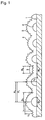
- the substrate with a transparent conductive oxide film of the present invention will be described with reference to Figs. 1 and 2.
- the substrate with a transparent conductive oxide film of the present invention, the process for its production and the photoelectric conversion device (hereinafter a specific example of a solar cell will be described) are not limited thereto.
- the substrate with a transparent conductive oxide film of the present invention has, on a glass substrate 1, macro-sized roughness (texture) formed by a plurality of discontinuous ridges 2 and a plurality of flat portions 3 filling gaps between such ridges, and has a structure wherein the outer surfaces of the ridges 2 and the flat portions 3 have microroughness (texture).
- macro-sized roughness texture
- the structure having two roughnesses as described above will be referred to as a double texture structure.
- the height H a of the ridge (the height from the top of the micron-size protrusions on the flat portions) is preferably from 0.2 to 2.0 ⁇ m, more preferably from 0.3 to 1.0 ⁇ m, further preferably from 0.4 to 0.7 ⁇ m.
- the spacing W a between the ridges (the distance of the flat portion between the adjacent ridges) is linearly preferably from 0 to 2.0 ⁇ m, more preferably at most 1.2 ⁇ m, further preferably at most 0.4 ⁇ m, particularly preferably at least 0.1 ⁇ m (every ridge is discontinuous).
- the plurality of ridges may have a discontinuous portion and a continuous portion, and the spacing W a between ridges being from 0 to 2.0 ⁇ m, means that there may be a portion where no flat portion is present.
- the basal plane diameter D a of the above ridge is preferably from 1.0 to 3.0 ⁇ m, more preferably from 1.0 to 2.0 ⁇ m.
- the pitch P a between the above ridges (the distance between the tops of the adjacent ridges) is linearly preferably from 0.1 to 2.0 ⁇ m, more preferably from 0.5 to 1.5 ⁇ m, further preferably from 0.7 to 1.2 ⁇ m.
- Fig. 2 An enlarged view of Fig. 1 showing the above-mentioned microroughness, is shown in Fig. 2.
- the height H b of a protrusion 10 is preferably from 0.05 to 0.2 ⁇ m, more preferably from 0.1 to 0.2 ⁇ m.
- the pitch P b between the protrusions is linearly preferably from 0.1 to 0.3 ⁇ m, more preferably from 0.1 to 0.2 ⁇ m.
- the basal plane diameter D b of the above protrusion 10 is preferably from 0.1 to 0.3 ⁇ m, more preferably from 0.15 to 0.3 ⁇ m, and the ratio of height H b /basal plane diameter D b of the protrusion 10 is preferably from 0.7 to 1.2, more preferably from 0.7 to 1.0.
- the outer surfaces of the ridges 2 and the flat portions 3 By making the outer surfaces of the ridges 2 and the flat portions 3 to have roughness (microroughness) smaller than the roughness (macro-sized roughness) of such ridges, it is possible to intensely scatter light with a short wavelength, whereby it becomes possible to effectively scatter light in a wide wavelength range as a whole. Namely, it is possible to scatter light with a long wavelength by ridges having large roughness and to scatter light with a short wavelength by the surface with small roughness.
- the substrate with a transparent conductive oxide film of the present invention has the following relation between the wavelength and the haze over the entire substrate. Namely, over a full wavelength region of from 400 to 800 nm, the haze is from 10 to 95%.
- the haze is preferably from 40 to 70% in a wavelength region of from 400 to 600 nm, particularly preferably from 20 to 40% in a wavelength region of from 600 to 800 nm. Further, the difference between the maximum value and the minimum value of the haze (the maximum value - the minimum value) is preferably not more than 50%.
- a substrate to be used as the substrate with a transparent conductive oxide film of the present invention is not necessarily required to be flat and a plate-shaped, and it may have a curved surface or an abnormal profile.
- a substrate may, for example, be a glass substrate, a ceramic substrate, a plastic substrate or a metal substrate.
- the substrate is preferably a transparent substrate excellent in optical transmittance, and it is preferably a glass substrate from the viewpoint of the strength and heat resistance.
- a transparent glass plate made of colorless transparent soda lime silicate glass, aluminosilicate glass, borate glass, lithium aluminosilicate glass, quartz glass, borosilicate glass substrate, no-alkali glass substrate or various other glass, may be employed.
- the glass substrate When it is used as a substrate for a solar cell, the glass substrate preferably has a thickness of from 0.2 to 6.0 mm. Within this range, the glass substrate has high strength and high optical transmittance. Further, the substrate preferably has a high optical transmittance, for example, an optical transmittance of at least 80%, in a wavelength region of from 350 to 800 nm. Further, it preferably has a sufficient insulating property and high chemical and physical durability.
- an alkali barrier layer such as a silicon oxide film, an aluminum oxide film or a zirconium oxide film, may be formed on the glass substrate surface.
- a layer to reduce the difference in the refractive index between the surface of the glass substrate and the layer formed thereon may further be formed.
- the alkali barrier layer to be formed on a soda lime glass substrate may, for example, be SiO 2 , or a mixed oxide film or a multilayer film of SiO 2 and SnO 2 , and the film thickness is preferably from 20 to 100 nm. If the film thickness is within this range, it is possible to control absorption and reflection of a transmitted light from the glass substrate.
- the multilayer film a film may be mentioned wherein a SnO 2 film and a SiO 2 film are sequentially deposited on a soda lime glass substrate, and the film thicknesses are preferably from 20 to 30 nm and from 20 to 40 nm, respectively.
- the thickness of the alkali barrier layer is preferably from 40 to 60 nm.
- the microroughness formed on the outer surface can be measured by the following methods.
- Protrusions on the film surface were observed by a scanning electron microscope (SEM), and from the obtained microscopic photograph, the basal plane diameters of the protrusions were measured. Further, the surface morphology of the film was observed by SEM and by an atomic force microscope (AFM), and from the obtained microscopic photograph, the surface morphology of the film and the heights of the protrusions were analyzed.
- SEM scanning electron microscope
- AFM atomic force microscope
- the coverage on the substrate by small ridges made of the first oxide was measured from the SEM photograph. A value obtained by dividing the area occupied by small ridges on the substrate by the area of the entire covered surface of the substrate was evaluated as the surface coverage.
- the substrate with a transparent conductive oxide film of the present invention may be such that a transparent conductive oxide film having the above-mentioned double texture structure may be formed on a transparent substrate, and the above structure may be formed by a single oxide, but preferably it is constituted by the first and second oxides which will be described hereinafter.
- the shape of the substrate with a transparent conductive oxide film of the present invention comprises the above ridges 2 and the flat portions 3, as shown in Fig. 1, and its construction is preferably such that the ridges 2 and the flat portions 3 are formed by discontinuous small ridges 4 made of the first oxide formed on a glass substrate 1 and a continuous layer 5 made of a second oxide 2, formed thereon.
- a soda lime glass substrate is heated to 500°C in a belt conveyor furnace, and on this glass substrate, 4 L/min of nitrogen gas containing 5 mol% of silane gas and 20 L/min of oxygen gas are simultaneously blown to form a silica film. Then, this glass substrate with a silica film is heated to 540°C, and tin tetrachloride, water and hydrogen chloride gas are simultaneously blown to form discontinuous small ridges made of a first oxide on the silica film.
- the surface coverage of the discontinuous small ridges made of the first oxide on the glass substrate is from 10 to 70%, and if the surface coverage is within this range, the haze will be from 10 to 95% over a full wavelength region of from 400 to 800 nm, such being preferred. Further, such surface coverage is preferably from 50 to 60%, and if the surface coverage is within this range, after formation of the second oxide, the haze will be from 40 to 70% (as an average of from 400 to 600 nm) or from 20 to 40% (as an average of from 600 to 800 nm), and the difference of the absolute values between the maximum value and the minimum value of the haze (the maximum value - the minimum value) will be not more than 50%, such being preferred.
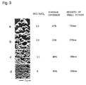
- the surface coverage can be adjusted by controlling the above-mentioned hydrogen chloride gas and the above-mentioned amount of water. As will be apparent from Examples given hereinafter, it is preferred to increase the proportion of hydrogen chloride gas to be added during formation of discontinuous small ridges made of the first oxide by the atmospheric pressure CVD method.
- the proportion of hydrogen chloride to be added is represented by the molar ratio of hydrogen chloride to tin tetrachloride (hereinafter referred to as HCl/SnCl 4 ), and HCl/SnCl 4 is preferably from 1.0 to 4.0. If HCl/SnCl 4 is within this range, small ridges can easily be formed, and the above-mentioned surface coverage can be controlled. It is particularly preferred that HCl/SnCl 4 is from 2.0 to 3.0.
- the above first oxide may be any oxide so long as it is highly transparent in a visible light region, and it may, for example, be SnO 2 , In 2 O 3 , ZnO, CdO, CdIn 2 O 4 , CdSnO 3 , MgIn 2 O 4 , CdGa 2 O 4 , GaInO 3 , InGaZnO 4 , Cd 2 Sb 2 O 7 , Cd 2 GeO 4 , CuAlO 2 , CuGaO 2 , SrCu 2 O 2 , TiO 2 or Al 2 O 3 .
- the refractive index is preferably from 1.8 to 2.2, more preferably from 1.9 to 2.1 at a wavelength of from 400 to 800 nm.
- the small ridges made of the above first oxide are discontinuous protrusions and not a continuous film. Therefore, at the transparent substrate portions not covered by such protrusions, the absorption loss of incident light by small ridges is, of course, 0, and thus, the amount of incident light to the photoelectric conversion layer can be increased.
- These small ridges are portions to increase the haze which will be described hereinafter (to increase the scattering degree of light) and preferably have no electrical conductivity in order to accomplish high transparency by suppressing absorption by free electrons. Accordingly, in a case where SnO 2 is used as the first oxide, it is preferred that the small ridges are made solely of SnO 2 , or in a case where they contain fluorine, the fluorine content is preferably not more than 0.01 mol%, more preferably not more than 0.005 mol%, based on SnO 2 .
- the second oxide layer will be described.
- the second oxide is preferably a transparent conductive oxide which is transparent in a visible light region and which further has electrical conductivity, and it may, for example, be SnO 2 , In 2 O 3 or ZnO containing a dopant to provide electrical conductivity.
- SnO 2 preferably contains fluorine or antimony as a dopant in an amount of from 0.01 to 4 mol% based on SnO 2 .
- ZnO preferably contains at least one member selected from the group consisting of B, Al and Ga, as a dopant, in an amount of from 0.02 to 5 mol% based on ZnO.
- In 2 O 3 preferably contains Sn in an amount of from 0.02 to 4 mol% based on In 2 O 3 .
- a halogen atom doped by a hydrogen halide may, for example, be HF, HCl, HBr or HI, but fluorine-doped SnO 2 is preferred. Specifically, it is for example preferred to have fluorine incorporated in an amount of from 0.01 to 4 mol%, more preferably from 0.1 to 1 mol%, to SnO 2 .
- the conductive electron density will be improved by using fluorine-doped SnO 2 as the above second oxide.
- the conductive electron density may be preferably within a range of from 5 ⁇ 10 19 to 4 ⁇ 10 20 cm -3 , more preferably within a range of from 1 ⁇ 10 20 to 2 ⁇ 10 20 cm -3 . Within this range, the amount of light absorption of the film is small, and the film is highly transparent and has high durability against active hydrogen species, whereby the transparency will not be lost by hydrogen plasma irradiation commonly employed at the time of forming a thin film silicon-type solar cell which will be described hereinafter.
- the height H c of the small ridge made of the first oxide is preferably from 0.2 to 2.0 ⁇ m, more preferably from 0.2 to 1.0 ⁇ m, further preferably from 0.4 to 0.7 ⁇ m.
- the distance W c between the small ridges is linearly preferably from 0.1 to 2.0 ⁇ m, more preferably from 0.1 to 1.5 ⁇ m.
- the basal plane diameter D c of the small ridge is preferably from 0.2 to 2.0 ⁇ m, more preferably from 0.2 to 1.0 ⁇ m
- the pitch P c between the small ridges is of the same value as P a and is linearly preferably from 0.1 to 2.0 ⁇ m, more preferably from 0.5 to 1.5 ⁇ m, further preferably from 0.7 to 1.2 ⁇ m.
- the continuous layer 5 made of the second oxide is continuously formed on the above small ridges 4 and on the glass substrate 1 where no small ridges 4 are formed.
- the surface of the continuous layer 5 has many micron-size protrusions 10 as mentioned above, and the thickness H d of the continuous layer 5 on the small ridges 4 (including the micron-size protrusions) is preferably from 0.5 to 1.0 ⁇ m, more preferably from 0.5 to 0.7 ⁇ m.
- the thickness H e of the continuous layer 5 on the glass substrate 1 (including the micron-size protrusions) is preferably from 0.5 to 1.0 ⁇ m, more preferably from 0.5 to 0.7 ⁇ m.
- the same oxide may be used for the first oxide and the second oxide, and it is preferred to use SnO 2 for each of them.
- the method for producing small ridges made of the first oxide on the substrate is not particularly limited.
- the oxide is formed by an atmospheric pressure CVD method, wherein a mixture of the metal chloride, a hydrogen halide and water, is used, whereby the metal element concentration in these media is adjusted.
- the amounts of the hydrogen halide and water are adjusted to the metal chloride.
- a thin oxide layer made of an oxide having a composition different from the first and second oxides may be formed between the first and second oxides, whereby the production can be made easily and certainly.
- a thin oxide layer (hereinafter referred to also as a different oxide layer) made of an oxide having a composition different from the first and second oxides on the surface of a flat glass substrate containing discontinuous small ridges made of the first oxide, the second oxide layer is deposited.
- a thin oxide layer hereinafter referred to also as a different oxide layer
- the second oxide layer is deposited.
- the different oxide layer is required to have high optical transmittance, and accordingly amorphous SiO 2 is more preferred.
- the film thickness is preferably from 2 to 40 nm, more preferably from 10 to 30 nm.
- a method for forming the different oxide layer and the second oxide layer will be shown below.
- a layer made of SiO 2 may, for example, be used.
- the layer made of SiO 2 is formed on the discontinuous small ridges made of the first oxide and on the flat glass substrate where no small ridges are formed.
- a glass substrate having small ridges made of the first oxide formed thereon is heated to 520°C, and on this glass substrate, 4 L/min of nitrogen gas containing 5 mol% of silane gas and 3 L/min of oxygen gas are simultaneously blown to form a layer made of amorphous SiO 2 by an atmospheric pressure CVD method. Further, this glass substrate is heated to 540°C, and tin tetrachloride, water, hydrogen fluoride and methanol are simultaneously blown thereto, and an atmospheric pressure CVD method is employed to form a fluorine (F)-doped SnO 2 transparent conductive oxide film as the second oxide layer.
- F fluorine
- the transparent conductive oxide as the second oxide may, for example, be F-doped SnO 2 , antimony-doped SnO 2 , Sn-doped In 2 O 3 (ITO), aluminum-doped ZnO or gallium-doped ZnO.
- the first oxide is preferably one formed to improve the haze
- the second oxide is preferably an oxide having electrical conductivity and high transparency.
- the refractive indices of the first oxide and the second oxide layer are preferably of an equal level and specifically at a level of from 1.8 to 2.2. If both the refractive indices of the first oxide and the second oxide are in this range, reflection of light at the interface between the first oxide and the second oxide will be controlled, whereby the optical transmittance will not decrease, such being desirable.
- the first oxide is preferably one to improve the haze.
- the second oxide layer formed as a continuous layer is preferably an oxide having electrical conductivity and high transparency.
- the substrate with a transparent conductive oxide film of the present invention is constituted by a plurality of ridges having the above-described shape and a plurality of flat portions filling spacing between the ridges, and the surfaces of the ridges and the flat portions have many continuous micron-size protrusions.
- the height from the substrate surface to the top of the ridge (including the micron-size protrusions) is preferably from 0.8 to 3.0 ⁇ m, more preferably from 0.8 to 1.0 ⁇ m, and the sheet resistance of the entire conductive film is preferably from 8 to 20 ⁇ / ⁇ , more preferably from 8 to 12 ⁇ / ⁇ .
- the optical transmittance (transparency) at 550 nm is preferably from 80 to 90%, more preferably from 85 to 90%, as measured by an immersion liquid method which will be described in detail in Examples given hereinafter. Further, as mentioned above, the haze is preferably from 10 to 95% over a full wavelength region of from 400 to 800 nm.
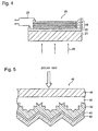
- a photoelectric conversion element of the present invention (hereinafter described as a solar cell) comprising the above-described substrate with a transparent conductive oxide film, a photoelectric conversion layer and a rear face electrode, will be described with reference to Fig. 4.
- the substrate with a transparent conductive oxide film of the present invention, the solar cell and the processes for their production are not limited thereto.
- the solar cell of the present invention is shown at 20 and has, on a glass substrate 21, a transparent conductive oxide film 22 to be used for the substrate with a transparent conductive oxide film of the present invention, a photoelectric conversion layer 26 and a rear face electrode 27.
- This construction is one of photoelectric conversion apparatus which can be produced at a relatively low cost.
- Such a solar cell 20 is designed so that light 28 enters from the glass substrate 21 side and is mainly absorbed within the i-type-layer 24.
- An electromotive force is generated between two electrodes i.e. the transparent conductive oxide film 22 and the rear face electrode 27, and the electricity will be taken out from the solar cell via a conductive wire 29.
- the photoelectric conversion layer 26 may be any layer so long as it is a photoelectric conversion layer which can be used for a common solar cell.
- the structure of the photoelectric conversion layer 26 shown in Fig. 4 is a single junction comprising three layers wherein a p-type-layer 23, an i-type-layer 24 and an n-type-layer 25 are formed in this order.
- the material for the p-type-layer may, for example, be hydrogenated amorphous silicon carbide (a-SiC:H), and the material for the i-type-layer may, for example, be hydrogenated amorphous silicon (a-Si:H), crystalline silicon (c-Si), microcrystalline silicon ( ⁇ c-Si), or hydrogenated amorphous silicon germanium (a-SiGe:H).
- the material for the n-type-layer may, for example, be hydrogenated amorphous silicon (a-Si:H) or microcrystalline silicon ( ⁇ c:Si).
- an electric power generation layer of a tandem structure wherein on the p-i-n-type-layer of a-Si, a still another p-i-n-type-layer is formed may, for example, be preferably used.
- an electromotive layer of a tandem structure wherein the layer formed on the p-i-n-type-layer of a-Si is three layers wherein an a-Si:H layer as the p-type-layer, a microcrystalline Si layer as the i-type-layer and an a-Si:H layer as the n-type-layer are formed in this order, or three layers wherein an a-Si:H layer as the p-type-layer, an a-SiGe:H layer as the i-type-layer and an a-Si:H layer as the n-type-layer are formed in this order.
- the electromotive layer of a tandem structure for the photoelectric conversion layer, photoelectric conversion of light on not only the short wavelength side but also on the long wavelength side will be possible. Accordingly, if the electromotive layer having such a tandem structure is employed on the substrate with a transparent conductive oxide film of the present invention having the double texture structure, the effect for improving the photoelectric conversion efficiency will be more distinct.
- a layer containing Ag or an Ag alloy, or Al or an Al alloy, as the main component may be used as the electrode material for the above back electrode layer 27 .
- a metal film containing crystalline Ag in an amount of at least 95 mol% in the film is employed.
- the above metal film may contain Pd and/or Au as a component.
- the content of Pd and Au in the film is preferably from 0.3 to 5 mol% each, more preferably from 0.3 to 3 mol% each, based on the sum with Ag.
- the total amount of impurities is preferably not more than 1 mol%.
- the solar cell of the present invention may have a contact-improving layer between the above back electrode layer 27 and the photoelectric conversion layer 26, as shown in Fig. 4.
- An embodiment of a substrate for a solar cell having the transparent conductive oxide film of the present invention and the contact-improving layer, will be described with reference to Fig. 5.
- the substrate with a transparent conductive oxide film of the present invention, the process for its production and the photoelectric conversion element are not limited thereto.
- the substrate for a solar cell is shown at 40 and comprises a glass substrate 44, the transparent conductive oxide film 45 of the present invention, a photoelectric conversion layer 42 made of a p-i-n-type-layer of a-Si, a contact-improving layer 41 and a rear face electrode 43.
- the contact-improving layer 41 is located between the above-mentioned p-i-n-type-layer of a-Si and the rear face electrode 43, as shown in Fig. 5, and is used to improve the contact of the photoelectric conversion layer represented by the p-i-n-type-layer of a-Si with the rear face electrode represented by the rear face electrode 43.
- the contact-improving layer 41 is preferably such that the resistivity and the absorption coefficient are small. Specifically, the resistivity is preferably at most 1 ⁇ 10 -2 ⁇ cm, more preferably at most 5 ⁇ 10 -3 ⁇ cm. If the resistivity of the above contact-improving layer 41 is within this range, it becomes possible to pass the electromotive force photoelectrically converted in the p-i-n-type-layer 42 of a-Si as the photoelectric conversion layer to the rear face electrode 43 as the rear face electrode without reducing it.
- the absorption coefficient is not more than 5 ⁇ 10 3 cm -1 , more preferably not more than 2 ⁇ 10 3 cm -1 in a wavelength region of from 500 to 800 nm. If the absorption coefficient of the above contact-improving layer 41 is within this range, it becomes possible to pass the light passed through the p-i-n-type-layer 42 of a-Si as the photoelectric conversion layer to the rear face electrode 43 as the rear side electrode without absorption.
- the material for the contact-improving layer 41 preferably contains zinc oxide (ZnO) as the main component, whereby at least 90 atomic% of the total metal component in the film is preferably Zn. More preferred is a layer having gallium (Ga) incorporated to the above layer containing zinc oxide as the main component, or a layer having aluminum (Al) incorporated thereto. By incorporating Ga or Al, the conductive electron density will be increased, and it serves as a dopant to zinc oxide, whereby it has an effect to improve the electroconductivity of the entire contact-improving layer 41.
- ZnO zinc oxide
- Ga gallium
- Al aluminum
- the content of Ga or Al is preferably from 0.3 to 10 mol%, more preferably from 0.3 to 5 mol%, based on the sum with Zn. If the content is within this range, it is possible to prevent an increase of the absorption coefficient of the contact-improving layer 41 due to an excessive improvement of the electroconductivity.
- the zinc oxide layer containing Ga or Al may contain impurities, and the total amount of impurities is preferably not more than 1 mol%.
- the present invention provides a process for forming the above-mentioned solar cell by means of a plasma-enhanced CVD method or a sputtering method.
- a method for forming a photoelectric conversion layer on the substrate with a transparent conductive oxide film of the present invention is the plasma-enhanced CVD method. Further, a method of forming the above-mentioned contact-improving layer and the above-mentioned rear face electrode on the above photoelectric conversion layer in this order, is the sputtering method.
- the plasma-enhanced CVD method may be carried out under the conditions for forming a photoelectric conversion layer in a common solar cell, and for example, the p-i-n-type-layer of a-Si may be formed under the condition shown in Examples given hereinafter.
- the sputtering method is a method for forming the above-mentioned contact-improving layer on the above photoelectric conversion layer. Specifically, it is a method for depositing a contact-improving layer on the photoelectric conversion layer by carrying out sputtering in an inert gas atmosphere using Ga-doped zinc oxide (hereinafter GZO) as a target.
- GZO Ga-doped zinc oxide
- the method for forming the GZO layer is not particularly limited, and a physical vapor deposition method such as a sputtering method or a vacuum vapor deposition method, or a chemical vapor deposition method such as a CVD method may be employed. However, it is preferred to employ a physical vapor deposition method, whereby good conductive film characteristics can be obtained at a lower substrate temperature. In the following Examples, a DC sputtering method is employed, but this may be carried out by a high frequency sputtering method.
- a method for depositing a back electrode layer on the GZO layer as the contact-improving layer by carrying out sputtering in an inert gas atmosphere employing a metal containing at least 95 mol% of Ag (hereinafter referred to as a Ag type metal) as a target is also a sputtering method.
- the solar cell of the present invention may be prepared, for example, as follows. Firstly, a GZO target to form the contact-improving layer is attached to a cathode of a DC magnetron sputtering equipment. Further, the substrate with a transparent conductive oxide film having a photoelectric conversion layer formed, is attached to the substrate holder. Then, the interior of the film-forming chamber is evacuated to vacuum, and then, argon gas is introduced as sputtering gas. As the sputtering gas, other than the argon gas, an inert gas such as He, Ne or Kr may be employed. However, it is preferred to use argon gas which is inexpensive and whereby the discharge is stable.
- an inert gas containing carbon dioxide in an amount of from 0.3 to 20 vol%, still more preferably from 0.3 to 10 vol%.
- the pressure during the sputtering is usually from 0.1 to 1.5 Pa. Further, the residual gas pressure is preferably from 1.0 ⁇ 10 -5 to 2.5 ⁇ 10 -3 Pa.
- the substrate temperature is usually from room temperature to 200°C, particularly from 100 to 150°C, from the viewpoint of the characteristics of the solar cell.
- inclined sputtering For the above film forming by sputtering, it is preferred to carry out sputtering by having the GZO target inclined at an angle of from 30 to 90° to the substrate (hereinafter referred to as inclined sputtering), whereby low resistance and low absorption can be accomplished simultaneously.
- the pressure during the sputtering is also similar and is usually from 0.1 to 1.5 Pa. Further, the residual gas pressure is preferably from 1.0 ⁇ 10 -5 to 2.5 ⁇ 10 -3 Pa.
- the temperature of the substrate during the sputtering is usually from room temperature to 200°C, particularly from 100°C to 150°C, from the viewpoint of the adhesion between the substrate and the film. It is preferred to heat the substrate during the sputtering, whereby improvement of crystallinity of Ag as the rear face electrode, improvement in the reflectance and reduction of the resistance of the entire substrate can be obtained.
- a Ag layer containing Pd and/or Au when a Ag layer containing Pd and/or Au is formed as the back electrode layer, separate targets may be used for Pd and/or Au, or an Ag alloy containing Pd and/or Au having a desired composition, may be preliminarily prepared, and such an alloy may be used as the target.
- the photoelectric conversion layer when it is a tandem structure having a separate p-i-n-type-layer formed on the p-i-n-type-layer of a-Si, it may have a tandem structure wherein the layer to be formed on the p-i-n-type-layer of a-Si is three layers wherein an a-Si:H layer as the p-type-layer, a microcrystalline Si layer as the i-type-layer and an a-Si:H layer as the n-type-layer, are formed in this order or three layers wherein an a-Si:H layer as the p-type-layer, an a-SiGe:H layer as the i-type-layer and an a-Si:H layer as the n-type-layer, are formed in this order.
- the film thickness of the photoelectric conversion layer varies depending upon the type of the electromotive layer to be formed.
- the thickness of the p-type-layer or the n-type-layer formed by the plasma-enhanced CVD method is within a range of from 5 to 15 nm, and the thickness of the i-type-layer is from 100 to 400 nm. Further, the thickness of the microcrystalline Si layer in the tandem structure is from 500 to 3000 nm.
- the thickness of the contact-improving layer formed by the sputtering method is preferably from 50 to 200 nm, more preferably from 50 to 150 nm.
- the film thickness is preferably from 50 to 150 nm. If the thickness of the contact-improving layer is within this range, an adequate effect for improving the contact can be obtained also for the double texture structure like the substrate with a transparent conductive oxide film of the present invention.
- the thickness of the back electrode layer is preferably from 100 to 300 nm, more preferably from 150 to 250 nm. Especially when the back electrode layer is Ag, the thickness is preferably from 150 to 250 nm.
- a substrate with a transparent conductive oxide film of the present invention having a double texture structure was prepared under the conditions as identified in the following Examples.
- Tin tetrachloride was preliminarily heated to 45°C and transferred onto the substrate by blowing nitrogen gas at a rate of 2 L/min. Further, water heated to 100°C was blown at a rate of 15 g/min, and hydrogen chloride gas was blown at a rate of 0.5 L/min to the substrate.
- the surface morphology of the film was observed by SEM, whereby SnO 2 as the first oxide was found to be not a continuous film but form small ridges being macro-sized roughness.
- a SEM image of the substrate as observed from directly above was image-processed and calculated, whereby the coverage of the glass substrate surface by SnO 2 forming the small ridges, was 60%, the heights H c of the small ridges made of SnO 2 were from 0.4 to 0.6 ⁇ m, the basal plane diameters D c of the small ridges made of SnO 2 were from 0.5 to 0.7 ⁇ m, the distances W c between the adjacent small ridges were from 0.2 to 0.5 ⁇ m, and the pitches P c between the adjacent small ridges were from 0.7 to 1.2 ⁇ m.
- the sheet resistance of the small ridges made of the first oxide was found to be at least 20 M ⁇ / ⁇ , the haze was found to be 55% (as an average of from 400 to 600 nm), or 70% (as an average of from 600 to 800 nm), and the optical transmittance at 550 nm measured by an immersion liquid method was 88%.
- a soda lime glass substrate of 300 mm ⁇ 300 mm ⁇ 1.1 mm in thickness was heated to 500°C in a belt conveyor furnace (speed of the belt: 1 m/min), and firstly, 4 L/min of nitrogen gas containing 5 mol% of silane gas and 20 L/min of oxygen gas were simultaneously blown thereto to form a silica film. Then, the glass substrate with this silica film, was heated to 540°C, and tin tetrachloride, water and hydrogen chloride gas were blown thereto in the proportions as identified below, to form SnO 2 as the first oxide.
- tin tetrachloride was preliminarily heated to 45°C and transferred onto the substrate by blowing nitrogen gas at a rate of 2 L/min.
- nitrogen gas was blown at a rate of 15 g/min and hydrogen chloride gas was blown at a rate of from 0 to 0.6 L/min to the substrate.
- Figs. 3a to 3d are electron microscopic photographs.
- an amorphous SiO 2 film as a different oxide layer was formed by means of an atmospheric pressure CVD method.
- the glass temperature was 520°C
- the amount of the nitrogen gas containing 5 mol% of silane gas was 0.6 L/min
- the amount of the oxygen gas was 3L/min.
- this substrate was heated to 540°C, and tin tetrachloride, water, HF gas and methanol were blown thereto to form a F-doped SnO 2 film as a second oxide layer.
- the tin tetrachloride was preliminarily heated to 45°C and transferred onto the substrate by blowing nitrogen gas at a rate of 12 L/min. Whereas, water heated to 100°C was blown at a rate of 90 g/min, and the HF gas was blown at a rate of 3 L/min to the substrate. Further, to the methanol preliminarily heated to 30°C, nitrogen gas was blown at a rate of 0.1 L/min, and the mixture was blown to the substrate.
- the surface morphology of the film was observed by SEM and AFM. According to the SEM observation, the F-doped SnO 2 film as the second oxide layer was found to be continuous layer, and the coverage of the glass substrate surface by the F-doped SnO 2 film was 100%.
- the heights H a of the ridges were from 0.4 to 0.6 ⁇ m
- the distances W a between the adjacent ridges were from 0 to 0.4 ⁇ m
- the basal plane diameters D a of the ridges were from 1.0 to 1.5 ⁇ m
- the pitches P a between the adjacent ridges were from 0.3 to 1.2 ⁇ m
- the heights from the substrate surface to the tops of the ridges were from 0.8 to 1.0 ⁇ m.
- the surface of the F-doped SnO 2 film had many micron-sized roughness, and the heights H b of the protrusions were from 0.1 to 0.2 ⁇ m, the pitches P b between the protrusions were from 0.1 to 0.2 ⁇ m, the basal plane diameters D b of the protrusions were from 0.2 to 0.3 ⁇ m, and the height H b /basal plane diameter D b of the protrusions was 0.73.
- the sheet resistance was found to be 10 ⁇ / ⁇
- the haze was found to be 65% (as an average of from 400 to 600 nm) or 30% (as an average of from 600 to 800 nm)
- the optical transmittance at 550 nm measured by an immersion liquid method was 87%.
- the electron density was obtained by measurement by the Hall effect (van der Pauw method) and found to be 1.5 ⁇ 10 20 cm -3 . Further, the thickness of the F-doped SnO 2 film was 0.6 ⁇ m as measured by a contact type film thickness meter.
- a silica film was prepared under the same manner as in Production Example 1, and then, the glass substrate with the silica film was heated to 540°C, and tin tetrachloride, water, and hydrogen chloride gas were simultaneously blown thereto to form SnO 2 as the first oxide.
- the tin tetrachloride was preliminarily heated to 45°C and transferred onto the substrate by blowing nitrogen gas at a rate of 4 L/min. Whereas, water heated to 100°C was blown at a rate of 30 g/min, and the hydrogen chloride gas was blown at a rate of 1.0 L/min to the substrate. Formation of the second oxide layer was carried out under the same manner as in Production Example 1.
- the roughness of the surface of the obtained film was observed by SEM and AFM. According to the SEM observation, like the film obtained in Example of Production Example 1, the F-doped SnO 2 film as the second oxide layer was a continuous layer, and the coverage of the glass substrate surface by the F-doped SnO 2 film was 100%.
- the heights H a of the ridges were from 0.8 to 1.2 ⁇ m
- the distances W a between the adjacent ridges were from 0 to 0.6 ⁇ m
- the basal plane diameters D a of the ridges were from 1.2 to 1.8 ⁇ m
- the pitches P a between the adjacent ridges were from 0.6 to 2.0 ⁇ m
- the heights from the substrate surface to the tops of the ridges were from 1.4 to 1.8 ⁇ m.
- the surface of the F-doped SnO 2 film had many micron-size irregularities
- the heights H b of the protrusions were from 0.1 to 0.2 ⁇ m
- the pitches P b between the protrusions were from 0.1 to 0.2 ⁇ m
- the basal plane diameters D b of the protrusions were from 0.2 to 0.3 ⁇ m
- the height H b /basal plane diameter D b of the protrusions was 0.73.
- the sheet resistance was found to be 11 ⁇ / ⁇ , and the haze was found to be 82% (as an average of from 400 to 600 nm) or 62% (as an average of from 600 to 800 nm), and the optical transmittance at 550 nm measured by an immersion liquid method was 86%.
- Figs. 6 and 7 Electron microscopic photographs of the film obtained in Example of the above Production Example 1 and the film obtained in Production Example 2 are shown in Figs. 6 and 7, respectively.
- Figs. 6A and Figs. 6B are electron microscopic photographs showing the surface morphology of the film shown by 20000 magnifications and 3500 magnifications, respectively.
- Fig. 7A and Fig. 7B are electron microscopic photographs showing the surface morphology of the film shown by 20000 magnifications and 3500 magnifications, respectively. From these photographs, it was found that the substrate with a transparent conductive oxide film of the present invention having a transparent conductive oxide film formed on a substrate has a double texture structure.
- the sheet resistance was measured by a four terminal method. A square of about 3 cm ⁇ 3 cm was cut out from the substrate with a conductive oxide film, and a pair of electrodes having a length of 3 cm were attached at the opposing two sides in parallel on the film so that the distance between the electrodes would be 3 cm. Then, the resistance between the electrodes was measured by a tester and taken as the sheet resistance. The haze was measured by means of a spectro-photometer (U3400, manufactured by Hitachi, Ltd.). The measured wavelength range was from 400 to 800 nm, the measured distance was 10 nm.
- the optical transmittance was measured by a normal transmission method.
- the optical transmittance at each wavelength is designated as Td( ⁇ ).
- an integrating sphere having an inner sphere diameter of 150 mm was mounted, and the film surface of the sample was closely contacted to the integrating sphere, and the integrating sphere optical transmittance was measured.
- the optical transmittance at each wavelength at that time is designated as Tt( ⁇ ).
- the spectral transmittance was measured by means of an immersion liquid method to minimize the measurement error due to the difference in the surface roughness of the conductive oxide substrate.
- the immersion liquid method is a method wherein a few drops of diiodomethane was dropped on the film surface of the substrate with the conductive oxide film, and the optical transmittance is measured by sandwiching the solution by a transparent quartz glass.
- the absorption by diiodomethane is mainly at most 400 nm. Accordingly, within a range of from 400 to 800 nm, there will be no substantial absorption by the diiodomethane and the quartz glass.
- the measurement of the spectral transmittance was carried out by mounting an integrating sphere having an inner sphere diameter of 150 mm (150-0901, manufactured by Hitachi, Ltd.) on a spectro-photometer (U3400, manufactured by Hitachi, Ltd.).
- FIG. 8A and B are electron microscopic photographs when on the first oxide (Fig. 8A), the second oxide layer was formed (Fig. 8B).
- a soda lime glass substrate of 300 mm ⁇ 300 mm ⁇ 1.1 mm in thickness was heated to 500°C in a belt conveyor furnace (speed of the belt: 1 m/min), and firstly, 4 L/min of nitrogen gas containing 5 mol% of silane gas and 20 L/min of oxygen gas were simultaneously blown thereto to form a silica film.
- this glass substrate with the silica film was heated to 540°C, and then tin tetrachloride, water and hydrogen chloride gas were simultaneously blown thereto to form SnO 2 as the first oxide.
- the tin tetrachloride was preliminarily heated to 45°C and transferred onto the substrate by blowing nitrogen gas at a rate of 2 L/min. Whereas, water heated to 100°C was blown at a rate of 15 g/min, and the hydrogen chloride gas was blown at a rate of 0.5 L/min to the substrate.
- the F-doped SnO 2 film as the second oxide layer was formed by heating this substrate to 540°C, followed by blowing tin tetrachloride, water, HF gas and methanol thereto.
- Table tin tetrachloride was preliminarily heated to 45°C and transferred onto the substrate by blowing nitrogen gas at a rate of 12 L/min. Whereas, water heated to 100°C was blown at a rate of 90 g/min, and the HF gas was blown at a rate of 3 L/min to the substrate. Further, 0.1 L/min of nitrogen gas was blown to methanol preliminarily heated to 30°C, and the mixture was blown to the substrate.
- the substrate with the transparent conductive oxide film obtained in Example of Production Example 1 was cut into a size of 40 mm ⁇ 40 mm, and a photoelectric conversion layer having p-i-n junction was laminated on the transparent conductive oxide film by a plasma-enhanced CVD equipment (SLCM14, manufactured by Shimadzu Corporation).
- Table p-i-n junction is one wherein the p-type-layer, the i-type-layer and the n-type-layer are formed (joined) in this order.
- Table film-forming conditions for the p-type-layer, the i-type-layer, the n-type-layer and the p/i buffer layer used in this test were shown in Table 1, 2, 3 and 4, respectively.
- a GZO layer was formed in a thickness of about 100 nm by a DC sputtering method by inclining a GZO target containing 5 mol% of Ga based on the sum with zinc at an angle of 60° to the substrate.
- the sputtering was carried out by preliminarily evacuating the vacuum apparatus to a reduced pressure of at most 10 -4 Pa and then introducing 75 sccm of Ar gas and 1 sccm of CO 2 gas, whereby the pressure during the sputtering was adjusted to be 4 ⁇ 10 -1 Pa, and the sputtering power was adjusted to be 2.4 W/cm 2 .
- the Ga content in the GZO film was 5 mol% based on the sum with zinc in the same content as in the target, and the substrate temperature was adjusted to be 100°C.
- the performance of the GZO single film was such that the resistivity was 5 ⁇ 10 -3 ⁇ cm, and the absorption coefficient was 1 ⁇ 10 3 cm -1 at from 500 to 800 nm.
- a Ag film as the back electrode layer was formed in a thickness of about 200 nm on the GZO film by a sputtering method in an Ar gas atmosphere using a Ag target (the pressure during the sputtering: 4 ⁇ 10 -1 Pa, sputtering power: 1.4 W/cm 2 ), and finally a solar cell having a size of 5 mm ⁇ 5 mm was prepared.
- the solar cell characteristics were obtained in the same manner as in the Production Example 1, whereby the short circuit current was 19.3 mA/cm 2 , the open circuit voltage was 0.81 V, the fill factor was 0.71, and the conversion efficiency was 11.1%.
- a photoelectric conversion layer was formed in the same manner as in Production Example 1 to obtain a solar cell.
- the solar cell obtained by the above method did not function as a solar cell.
- the substrate with a transparent conductive oxide film having a double texture structure, obtained by the present invention has low resistance and high transparency and is excellent in mass productivity, and it has good light scattering performance over a full wavelength region of solar ray (from 300 nm to 3 ⁇ m). Further, according to the process of the present invention, such a substrate can be obtained with good productivity. If this substrate is used as a substrate for a thin film silicon type photoelectric conversion element, it is possible to obtain a photoelectric conversion element (especially a solar cell) excellent in the photoelectric conversion efficiency.
Landscapes
- Chemical & Material Sciences (AREA)
- Metallurgy (AREA)
- Chemical Kinetics & Catalysis (AREA)
- Engineering & Computer Science (AREA)
- Materials Engineering (AREA)
- Mechanical Engineering (AREA)
- General Chemical & Material Sciences (AREA)
- Organic Chemistry (AREA)
- Inorganic Chemistry (AREA)
- Photovoltaic Devices (AREA)
- Non-Insulated Conductors (AREA)
- Laminated Bodies (AREA)
- Manufacturing Of Electric Cables (AREA)
Abstract
Description
- 1:
- glass substrate
- 3:
- flat portion
- 5:
- continuous layer
- Wa:
- distance between ridges
- Wc:
- distance between small ridges
- Ha:
- height of ridge
- Hc:
- height of small ridge
- 2:
- ridge
- 4:
- small ridge
- 10:
- protrusion
- Hb:
- height of protrusion
- Hd, He:
- thickness of continuous layer
- Da:
- basal plane diameter of ridge
- Db:
- basal plane diameter of protrusion
- Dc:
- basal plane diameter of small ridge
- Pa:
- pitch between ridges
- Pb:
- pitch between protrusions
- Pc:
- pitch between small ridges
- 20:
- solar cell
- 21:
- transparent insulating substrate
- 22:
- transparent conductive film
- 23:
- p-type-layer
- 24:
- i-type-layer
- 25:
- n-type-layer
- 26:
- photoelectric conversion layer
- 27:
- rear face electrode
- 28:
- light
- 29:
- conductor wire
- 40:
- substrate for solar cell
- 41:
- contact-improving layer
- 42:
- p-i-n-type-layer of a-Si
- 43:
- rear face electrode
- 44:
- glass substrate
- 45:
- transparent conductive oxide film
| Deposition condition of p-type-layer | |||
| Substrate surface temperature | 180° | ||
| Pressure | |||
| 40 Pa | |||
| RF power | 0.03 W/cm2 | ||
| Gas | SIH | 4 | 10 |
| CH | |||
| 4 | 20 | ||
| H | |||
| 2 | 20 sccm | ||
| H2/B2H6 | 100 sccm | ||
| (B2H6: 1000 ppm) |
| Deposition condition of i-type-layer | |
| Substrate surface temperature | 180° |
| Pressure | |
| 27 Pa | |
| RF power | 0.03 W/cm2 |
| Gas | 10 sccm |
| Deposition condition of n-type-layer | |||
| Substrate surface temperature | 180° | ||
| Pressure | |||
| 40 Pa | |||
| RF power | 0.03 W/cm2 | ||
| Gas | SiH | 4 | 10 sccm |
| H2 | 100 sccm | ||
| H2/PH3 | 100 sccm | ||
| (PH3: 1000 ppm) |
| Deposition condition of p/i buffer layer | |||
| Substrate surface temperature | 180° | ||
| Pressure | |||
| 27 Pa | |||
| RF power | 0.03 W/cm2 | ||
| Gas | SiH | 4 | 10 |
| CH | |||
| 4 | 0 to 20 | ||
| H | |||
| 2 | 20 sccm |
| Thickness of p-type- | 10 nm |
| Thickness of p-SiC buffer layer | 8 nm |
| Thickness of i-type-layer | 350 nm |
| Thickness of n-type- | 40 nm |
| Thickness of | 10 nm |
| Thickness of Ag layer | 200 nm |
Claims (26)
- A substrate with a transparent conductive oxide film, comprising a substrate and a transparent conductive oxide film provided on the substrate and constituted by a plurality of ridges and a plurality of flat portions, wherein the surfaces of the ridges and the flat portions have many continuous micron-size protrusions.
- The substrate with a transparent conductive oxide film according to Claim 1, wherein the protrusions have basal plane diameters of from 0.1 to 0.3 µm and height/basal plane diameter ratios of from 0.7 to 1.2.
- A substrate with a transparent conductive oxide film, comprising a substrate and a transparent conductive oxide film provided on the substrate, wherein the substrate with the transparent conductive oxide film, has a haze of from 10 to 95% over a full wavelength region of from 400 to 800 nm, and the difference of the absolute values between the maximum value and the minimum value of the haze (the maximum value - the minimum value) is not more than 50%.
- The substrate with a transparent conductive oxide film according to Claim 3, wherein the substrate with the transparent conductive oxide film, has a haze of from 40 to 70% (as an average of from 400 to 600 nm) in a wavelength region of from 400 to 600 nm and a haze of from 20 to 40% (as an average of from 600 to 800 nm) in a wavelength region of from 600 to 800 nm.
- A substrate with a transparent conductive oxide film, comprising a substrate and a transparent conductive oxide film provided on the substrate, wherein the transparent conductive oxide film comprises discontinuous small ridges made of a first oxide and a continuous layer made of a second oxide, formed on the small ridges, wherein the surface of the continuous layer has many continuous micron-size protrusions.
- The substrate with a transparent conductive oxide film according to any one of Claims 1 to 5, wherein the substrate with the transparent conductive oxide film, has a sheet resistance of from 8 to 20 Ω/□ and an optical transmittance of from 80 to 90% at 550 nm measured by an immersion liquid method.
- The substrate with a transparent conductive oxide film according to Claim 5, wherein the small ridges have basal plane diameters of from 0.2 to 2.0 µm.
- The substrate with a transparent conductive oxide film according to Claim 5, wherein the first oxide is composed of SnO2 or SnO2 containing fluorine, the fluorine content being not more than 0.01 mol% based on SnO2.
- The substrate with a transparent conductive oxide film according to any one of Claims 5 to 8, wherein the second oxide is a transparent conductive oxide containing at least one member selected from the group consisting of SnO2, ZnO and In2O3.
- The substrate with a transparent conductive oxide film according to any one of Claims 5 to 9, wherein the second oxide is SnO2 containing fluorine-doped tin as the main component, contains fluorine in an amount of from 0.01 to 4 mol% based on SnO2 and has a conductive electron density of from 5×10¹⁹ to 4×1020 cm-3.
- The substrate with a transparent conductive oxide film according to any one of Claims 5 to 10, wherein a film made of an oxide different in the composition from the first and second oxides, is formed between the discontinuous small ridges made of the first oxide and the continuous layer made of the second oxide.
- The substrate with a transparent conductive oxide film according to Claim 11, wherein the first oxide is SnO2, the different oxide is SiO2, and the second oxide is fluorine-doped SnO2.
- The substrate with a transparent conductive oxide film according to Claim 1, 2, 5, 6, 7, 8, 9, 10, 11 or 12, wherein the substrate with the transparent conductive oxide film, has a haze of from 10 to 95% over a full wavelength region of from 400 to 800 nm.
- A process for producing the substrate with the transparent conductive oxide film as defined in any one of Claims 1 to 13, which comprises forming, on a transparent substrate, discontinuous small ridges made of a first oxide by an atmospheric pressure CVD method, and forming thereon a continuous layer made of a second oxide.
- The process for producing the substrate with the transparent conductive oxide film according to Claim 14, wherein the small ridges are formed by an atmospheric pressure CVD method employing tin tetrachloride, water and hydrogen chloride.
- The process for producing the substrate with the transparent conductive oxide film according to Claim 14, wherein the continuous layer made of the second oxide is formed on the discontinuous small ridges made of the first oxide, by an atmospheric pressure CVD method.
- The process for producing the substrate with the transparent conductive oxide film according to Claim 16, wherein a film made of an oxide different in the composition from the first and second oxides, is formed between the discontinuous small ridges made of the first oxide and the continuous layer made of the second oxide, by an atmospheric pressure CVD method.
- A photoelectric conversion element having a rear face electrode, via a photoelectric conversion layer, on the substrate with the transparent conductive oxide film as defined in any one of Claims 1 to 13.
- The photoelectric conversion element according to Claim 18, wherein the photoelectric conversion layer is a layer having p-, i- and n-type-layers formed in this order.
- The photoelectric conversion element according to Claim 18, wherein the rear face electrode is a metal film containing Ag in an amount of at least 95 mol% in the film.
- The photoelectric conversion element according to Claim 20, wherein the metal film contains Pd or Au in an amount of from 0.3 to 5 mol% in the film.
- The photoelectric conversion element according to any one of Claims 18 to 21, which has a contact-improving layer between the rear face electrode and the n-type-layer nearest to the rear face electrode, between the photoelectric conversion layer and the rear face electrode.
- The photoelectric conversion element according to Claim 22, wherein the contact-improving layer has a resistivity of not more than 1×10⁻² Ω·cm.
- The photoelectric conversion element according to Claim 22 or 23, wherein the contact-improving layer has an absorption coefficient of not more than 5×103 cm-1 in a wavelength region of from 500 to 800 nm.
- The photoelectric conversion element according to any one of Claims 22 to 24, wherein the contact-improving layer contains zinc oxide (ZnO) as the main component, and at least 90 atomic % of the total metal component in the layer is Zn.
- The photoelectric conversion element according to Claim 25, wherein the layer containing ZnO as the main component, contains Ga or Al in an amount of from 0.3 to 10 mol% based on the summation with Zn.
Applications Claiming Priority (3)
| Application Number | Priority Date | Filing Date | Title |
|---|---|---|---|
| JP2001322552 | 2001-10-19 | ||
| JP2001322552 | 2001-10-19 | ||
| PCT/JP2002/010801 WO2003036657A1 (en) | 2001-10-19 | 2002-10-17 | Substrate with transparent conductive oxide film and production method therefor, and photoelectric conversion element |
Publications (2)
| Publication Number | Publication Date |
|---|---|
| EP1443527A1 true EP1443527A1 (en) | 2004-08-04 |
| EP1443527A4 EP1443527A4 (en) | 2007-09-12 |
Family
ID=19139587
Family Applications (1)
| Application Number | Title | Priority Date | Filing Date |
|---|---|---|---|
| EP02775364A Withdrawn EP1443527A4 (en) | 2001-10-19 | 2002-10-17 | TRANSPARENT CONDUCTIVE OXIDE LAYER SUBSTRATE, PROCESS FOR PRODUCING THE SAME, AND PHOTOELECTRIC CONVERSION ELEMENT |
Country Status (4)
| Country | Link |
|---|---|
| US (3) | US7179527B2 (en) |
| EP (1) | EP1443527A4 (en) |
| JP (2) | JP4389585B2 (en) |
| WO (1) | WO2003036657A1 (en) |
Cited By (16)
| Publication number | Priority date | Publication date | Assignee | Title |
|---|---|---|---|---|
| EP1840966A1 (en) * | 2006-03-30 | 2007-10-03 | Universite De Neuchatel | Transparent, conducting and textured layer and method of fabrication |
| FR2915834A1 (en) * | 2007-05-04 | 2008-11-07 | Saint Gobain | TRANSPARENT SUBSTRATE WITH IMPROVED ELECTRODE LAYER |
| EP1724840A4 (en) * | 2004-02-20 | 2009-12-23 | Sharp Kk | SUBSTRATE FOR A PHOTOELECTRIC TRANSFORMER, PHOTOELECTRIC TRANSFORMER AND MULTILAYER PHOTOELECTRIC TRANSFORMER |
| WO2010039341A3 (en) * | 2008-10-02 | 2011-01-20 | Guardian Industries Corp. | Front electrode having etched surface for use in photovoltaic device and method of making same |
| CN102163648A (en) * | 2010-02-12 | 2011-08-24 | 住友重机械工业株式会社 | Manufacture method for solar cell and solar cell |
| WO2011161632A1 (en) | 2010-06-23 | 2011-12-29 | Commissariat A L'energie Atomique Et Aux Energies Alternatives | Substrate comprising a transparent conductive oxide film and its manufacturing process |
| EP2312642A4 (en) * | 2008-08-05 | 2012-01-11 | Asahi Glass Co Ltd | TRANSPARENT CONDUCTIVE FILM SUBSTRATE AND SOLAR CELL USING THE SUBSTRATE |
| WO2011161010A3 (en) * | 2010-06-21 | 2012-03-08 | Solayer Gmbh | Substrate with superficially structured surface electrode for a solar cell and method for producing said substrate |
| WO2011056570A3 (en) * | 2009-10-28 | 2012-10-26 | Corning Incorporated | Conductive metal oxide films and photovoltaic devices |
| AU2007346981B2 (en) * | 2007-02-16 | 2013-08-22 | Mitsubishi Heavy Industries, Ltd. | Photovoltaic device and process for producing same |
| WO2012148767A3 (en) * | 2011-04-29 | 2013-08-29 | Corning Incorporated | Photovoltaic device with surface perturbations configured for resonant and diffusive coupling |
| RU2505888C1 (en) * | 2012-07-31 | 2014-01-27 | Федеральное государственное бюджетное учреждение науки Физико-технический институт им. А.Ф. Иоффе Российской академии наук | Method of producing layer of transparent conducting oxide on glass substrate |
| WO2013189932A3 (en) * | 2012-06-19 | 2014-03-20 | Wilhelm Stein | Method and production system for producing a photovoltaic module, and photovoltaic module |
| EP2668670A4 (en) * | 2011-01-26 | 2014-07-23 | Lg Innotek Co Ltd | SOLAR CELL AND METHOD FOR MANUFACTURING SAME |
| EP2704226A3 (en) * | 2012-06-22 | 2017-03-01 | Corning Precision Materials Co., Ltd. | Substrate for oled and method of manufacturing the same |
| US10811845B2 (en) | 2012-02-28 | 2020-10-20 | Thorlabs Quantum Electronics, Inc. | Surface emitting multiwavelength distributed-feedback concentric ring lasers |
Families Citing this family (152)
| Publication number | Priority date | Publication date | Assignee | Title |
|---|---|---|---|---|
| WO2003036657A1 (en) * | 2001-10-19 | 2003-05-01 | Asahi Glass Company, Limited | Substrate with transparent conductive oxide film and production method therefor, and photoelectric conversion element |
| US7259085B2 (en) * | 2001-12-03 | 2007-08-21 | Nippon Sheet Glass Company, Limited | Method for forming thin film, substrate having thin film formed by the method, and photoelectric conversion device using the substrate |
| WO2003054974A1 (en) * | 2001-12-13 | 2003-07-03 | Asahi Glass Company, Limited | Cover glass for a solar battery |
| JP2005135942A (en) * | 2003-10-28 | 2005-05-26 | Canon Inc | Electrode placement method |
| US7608294B2 (en) | 2003-11-18 | 2009-10-27 | Nippon Sheet Glass Company, Limited | Transparent substrate with transparent conductive film, method of manufacturing the same, and photoelectric conversion element including the substrate |
| JP2005197608A (en) * | 2004-01-09 | 2005-07-21 | Mitsubishi Heavy Ind Ltd | Photoelectric converting device |
| JP2005347490A (en) * | 2004-06-02 | 2005-12-15 | Asahi Glass Co Ltd | Substrate with transparent conductive oxide film, method for producing the same, and photoelectric conversion element |
| ATE377580T1 (en) | 2004-07-12 | 2007-11-15 | Cardinal Cg Co | LOW MAINTENANCE COATINGS |
| EP1834933A4 (en) * | 2004-11-19 | 2009-04-01 | Nippon Sheet Glass Co Ltd | Process for producing glass plate with thin film |
| US20060211272A1 (en) * | 2005-03-17 | 2006-09-21 | The Regents Of The University Of California | Architecture for high efficiency polymer photovoltaic cells using an optical spacer |
| KR100638819B1 (en) * | 2005-05-19 | 2006-10-27 | 삼성전기주식회사 | Vertical nitride semiconductor light emitting device with improved light extraction efficiency |
| JP3954085B2 (en) * | 2005-10-07 | 2007-08-08 | シャープ株式会社 | Photoelectric conversion element and solar cell using the same |
| WO2007121215A1 (en) * | 2006-04-11 | 2007-10-25 | Cardinal Cg Company | Photocatalytic coatings having improved low-maintenance properties |
| EP1863100A1 (en) * | 2006-05-30 | 2007-12-05 | INTERUNIVERSITAIR MICROELEKTRONICA CENTRUM vzw (IMEC) | Method for the production of thin substrates |
| US20070256732A1 (en) * | 2006-05-02 | 2007-11-08 | Ming-Hsien Shen | Photovoltaic module |
| US8017860B2 (en) | 2006-05-15 | 2011-09-13 | Stion Corporation | Method and structure for thin film photovoltaic materials using bulk semiconductor materials |
| US7655542B2 (en) * | 2006-06-23 | 2010-02-02 | Applied Materials, Inc. | Methods and apparatus for depositing a microcrystalline silicon film for photovoltaic device |
| JP5000937B2 (en) * | 2006-06-30 | 2012-08-15 | 三菱電機株式会社 | Manufacturing method of semiconductor device |
| US7955889B1 (en) * | 2006-07-11 | 2011-06-07 | The Trustees Of Princeton University | Organic photosensitive cells grown on rough electrode with nano-scale morphology control |
| US20080011599A1 (en) | 2006-07-12 | 2008-01-17 | Brabender Dennis M | Sputtering apparatus including novel target mounting and/or control |
| JP5328083B2 (en) | 2006-08-01 | 2013-10-30 | キヤノン株式会社 | Oxide etching method |
| EP2381745A1 (en) * | 2006-09-07 | 2011-10-26 | Saint-Gobain Glass France | Substrate for organic electroluminescent device, use and method for manufacturing said substrate, as well as an organic electroluminescent device |
| US7854853B2 (en) * | 2006-11-09 | 2010-12-21 | Postech Academy-Industry Foundation | Nano fabrication method for glass |
| CN102941711B (en) * | 2006-11-17 | 2016-08-24 | 法国圣-戈班玻璃公司 | For the electrode of organic light emitting apparatus, its acid etching and the organic light emitting apparatus including it |
| US20080153280A1 (en) * | 2006-12-21 | 2008-06-26 | Applied Materials, Inc. | Reactive sputter deposition of a transparent conductive film |
| US8203071B2 (en) | 2007-01-18 | 2012-06-19 | Applied Materials, Inc. | Multi-junction solar cells and methods and apparatuses for forming the same |
| FR2913146B1 (en) * | 2007-02-23 | 2009-05-01 | Saint Gobain | DISCONTINUOUS ELECTRODE, ORGANIC ELECTROLUMINESCENCE DEVICE INCORPORATING THE SAME, AND THEIR MANUFACTURING |
| US20080245414A1 (en) * | 2007-04-09 | 2008-10-09 | Shuran Sheng | Methods for forming a photovoltaic device with low contact resistance |
| KR100843386B1 (en) * | 2007-04-12 | 2008-07-03 | 비오이 하이디스 테크놀로지 주식회사 | Manufacturing method of liquid crystal display device |
| US20080300918A1 (en) * | 2007-05-29 | 2008-12-04 | Commercenet Consortium, Inc. | System and method for facilitating hospital scheduling and support |
| US8071179B2 (en) | 2007-06-29 | 2011-12-06 | Stion Corporation | Methods for infusing one or more materials into nano-voids if nanoporous or nanostructured materials |
| US7875486B2 (en) * | 2007-07-10 | 2011-01-25 | Applied Materials, Inc. | Solar cells and methods and apparatuses for forming the same including I-layer and N-layer chamber cleaning |
| JP5022137B2 (en) * | 2007-08-06 | 2012-09-12 | 三菱重工業株式会社 | Manufacturing method and inspection method of photoelectric conversion device |
| JP2007311825A (en) * | 2007-08-06 | 2007-11-29 | Mitsubishi Heavy Ind Ltd | Photoelectric conversion device, and method of manufacturing the same |
| JP2007288223A (en) * | 2007-08-06 | 2007-11-01 | Mitsubishi Heavy Ind Ltd | Photoelectric conversion apparatus, and manufacturing method of photoelectric conversion apparatus |
| JP4852497B2 (en) * | 2007-08-27 | 2012-01-11 | 富士フイルム株式会社 | Solid-state image sensor |
| CA2664369A1 (en) | 2007-09-14 | 2009-03-19 | Cardinal Cg Company | Low-maintenance coatings, and methods for producing low-maintenance coatings |
| MY157221A (en) * | 2007-09-25 | 2016-05-13 | First Solar Inc | Photovoltaic devices including an interfacial layer |
| US8287942B1 (en) | 2007-09-28 | 2012-10-16 | Stion Corporation | Method for manufacture of semiconductor bearing thin film material |
| US8759671B2 (en) * | 2007-09-28 | 2014-06-24 | Stion Corporation | Thin film metal oxide bearing semiconductor material for single junction solar cell devices |
| US20090104733A1 (en) * | 2007-10-22 | 2009-04-23 | Yong Kee Chae | Microcrystalline silicon deposition for thin film solar applications |
| US7741144B2 (en) | 2007-11-02 | 2010-06-22 | Applied Materials, Inc. | Plasma treatment between deposition processes |
| US7998762B1 (en) | 2007-11-14 | 2011-08-16 | Stion Corporation | Method and system for large scale manufacture of thin film photovoltaic devices using multi-chamber configuration |
| FR2924274B1 (en) * | 2007-11-22 | 2012-11-30 | Saint Gobain | SUBSTRATE CARRYING AN ELECTRODE, ORGANIC ELECTROLUMINESCENT DEVICE INCORPORATING IT, AND MANUFACTURING THE SAME |
| FR2925981B1 (en) * | 2007-12-27 | 2010-02-19 | Saint Gobain | CARRIER SUBSTRATE OF AN ELECTRODE, ORGANIC ELECTROLUMINESCENT DEVICE INCORPORATING IT. |
| GB0803702D0 (en) | 2008-02-28 | 2008-04-09 | Isis Innovation | Transparent conducting oxides |
| KR101079612B1 (en) * | 2008-03-27 | 2011-11-03 | 주성엔지니어링(주) | Thin film type Solar Cell, and Method for manufacturing the same |
| US8642138B2 (en) | 2008-06-11 | 2014-02-04 | Stion Corporation | Processing method for cleaning sulfur entities of contact regions |
| US9087943B2 (en) * | 2008-06-25 | 2015-07-21 | Stion Corporation | High efficiency photovoltaic cell and manufacturing method free of metal disulfide barrier material |
| US8003432B2 (en) | 2008-06-25 | 2011-08-23 | Stion Corporation | Consumable adhesive layer for thin film photovoltaic material |
| US7855089B2 (en) * | 2008-09-10 | 2010-12-21 | Stion Corporation | Application specific solar cell and method for manufacture using thin film photovoltaic materials |
| FR2936358B1 (en) | 2008-09-24 | 2011-01-21 | Saint Gobain | PROCESS FOR MANUFACTURING SUBMILLIMETRIC MOLDED MASKS FOR SUBMILLIMETRIC ELECTROCONDUCTIVE GRID, SUBMILLIMETRIC MOLDING MASK, SUBMILLIMETRIC ELECTROCONDUCTIVE GRID. |
| FR2936362B1 (en) | 2008-09-25 | 2010-09-10 | Saint Gobain | METHOD FOR MANUFACTURING AN ELECTROCONDUCTIVE SUBMILLIMETRIC GRID COATED WITH A SURGRILLE GRID, ELECTROCONDUCTIVE SUBMILLIMETER GRID COVERED WITH AN OVERGRILL |
| US8008110B1 (en) | 2008-09-29 | 2011-08-30 | Stion Corporation | Bulk sodium species treatment of thin film photovoltaic cell and manufacturing method |
| US8026122B1 (en) | 2008-09-29 | 2011-09-27 | Stion Corporation | Metal species surface treatment of thin film photovoltaic cell and manufacturing method |
| US8236597B1 (en) | 2008-09-29 | 2012-08-07 | Stion Corporation | Bulk metal species treatment of thin film photovoltaic cell and manufacturing method |
| US8501521B1 (en) | 2008-09-29 | 2013-08-06 | Stion Corporation | Copper species surface treatment of thin film photovoltaic cell and manufacturing method |
| US8008112B1 (en) | 2008-09-29 | 2011-08-30 | Stion Corporation | Bulk chloride species treatment of thin film photovoltaic cell and manufacturing method |
| US8476104B1 (en) | 2008-09-29 | 2013-07-02 | Stion Corporation | Sodium species surface treatment of thin film photovoltaic cell and manufacturing method |
| US8394662B1 (en) | 2008-09-29 | 2013-03-12 | Stion Corporation | Chloride species surface treatment of thin film photovoltaic cell and manufacturing method |
| US8425739B1 (en) | 2008-09-30 | 2013-04-23 | Stion Corporation | In chamber sodium doping process and system for large scale cigs based thin film photovoltaic materials |
| US7863074B2 (en) * | 2008-09-30 | 2011-01-04 | Stion Corporation | Patterning electrode materials free from berm structures for thin film photovoltaic cells |
| US7947524B2 (en) * | 2008-09-30 | 2011-05-24 | Stion Corporation | Humidity control and method for thin film photovoltaic materials |
| US20110174361A1 (en) * | 2008-09-30 | 2011-07-21 | Jung-Sik Bang | Transparent conductive layer and transparent electrode comprising the same |
| US7910399B1 (en) * | 2008-09-30 | 2011-03-22 | Stion Corporation | Thermal management and method for large scale processing of CIS and/or CIGS based thin films overlying glass substrates |
| US8383450B2 (en) * | 2008-09-30 | 2013-02-26 | Stion Corporation | Large scale chemical bath system and method for cadmium sulfide processing of thin film photovoltaic materials |
| US8741689B2 (en) * | 2008-10-01 | 2014-06-03 | Stion Corporation | Thermal pre-treatment process for soda lime glass substrate for thin film photovoltaic materials |
| US20110018103A1 (en) | 2008-10-02 | 2011-01-27 | Stion Corporation | System and method for transferring substrates in large scale processing of cigs and/or cis devices |
| US8435826B1 (en) | 2008-10-06 | 2013-05-07 | Stion Corporation | Bulk sulfide species treatment of thin film photovoltaic cell and manufacturing method |
| US8003430B1 (en) | 2008-10-06 | 2011-08-23 | Stion Corporation | Sulfide species treatment of thin film photovoltaic cell and manufacturing method |
| US8168463B2 (en) | 2008-10-17 | 2012-05-01 | Stion Corporation | Zinc oxide film method and structure for CIGS cell |
| US8344243B2 (en) * | 2008-11-20 | 2013-01-01 | Stion Corporation | Method and structure for thin film photovoltaic cell using similar material junction |
| CN102257631A (en) * | 2008-12-26 | 2011-11-23 | 周星工程股份有限公司 | Thin-film solar cell and method for manufacturing same |
| US20110259410A1 (en) * | 2009-01-19 | 2011-10-27 | Oerlikon Solar Ag, Truebbach | Thin-film silicon tandem cell |
| TW201030994A (en) * | 2009-02-12 | 2010-08-16 | Nexpower Technology Corp | Two sided light absorbing type solar cell |
| CN101582461B (en) * | 2009-03-24 | 2012-05-02 | 新奥光伏能源有限公司 | Novel multilayer transparent conductive film structure and preparation method thereof |
| CN101582460B (en) * | 2009-03-24 | 2012-05-02 | 新奥光伏能源有限公司 | Multilayer transparent conductive film of thin film solar cell and manufacturing method thereof |
| FR2944145B1 (en) | 2009-04-02 | 2011-08-26 | Saint Gobain | METHOD FOR MANUFACTURING TEXTURED SURFACE STRUCTURE FOR ORGANIC ELECTROLUMINESCENT DIODE DEVICE AND STRUCTURE WITH TEXTURED SURFACE |
| US8241943B1 (en) | 2009-05-08 | 2012-08-14 | Stion Corporation | Sodium doping method and system for shaped CIGS/CIS based thin film solar cells |
| US8372684B1 (en) | 2009-05-14 | 2013-02-12 | Stion Corporation | Method and system for selenization in fabricating CIGS/CIS solar cells |
| US8519435B2 (en) | 2009-06-08 | 2013-08-27 | The University Of Toledo | Flexible photovoltaic cells having a polyimide material layer and method of producing same |
| JP2012531051A (en) * | 2009-06-22 | 2012-12-06 | ファースト ソーラー インコーポレイテッド | Method and apparatus for annealing deposited cadmium stannate layer |
| US8507786B1 (en) | 2009-06-27 | 2013-08-13 | Stion Corporation | Manufacturing method for patterning CIGS/CIS solar cells |
| CN102473748B (en) * | 2009-07-01 | 2014-08-20 | 三菱电机株式会社 | Thin film solar cell and manufacturing method thereof |
| CN102473750B (en) * | 2009-07-03 | 2014-08-20 | 株式会社钟化 | Crystalline silicon type solar cell and process for manufacture thereof |
| TWI411114B (en) * | 2009-07-10 | 2013-10-01 | Nexpower Technology Corp | A solar cell structure with discontinuous stacks |
| IN2012DN01226A (en) * | 2009-07-29 | 2015-04-10 | Asahi Glass Co Ltd | |
| US8398772B1 (en) | 2009-08-18 | 2013-03-19 | Stion Corporation | Method and structure for processing thin film PV cells with improved temperature uniformity |
| GB0915376D0 (en) | 2009-09-03 | 2009-10-07 | Isis Innovation | Transparent conducting oxides |
| US8558106B2 (en) * | 2009-10-20 | 2013-10-15 | Industrial Technology Research Institute | Solar cell device and method for fabricating the same |
| DE102009050234A1 (en) * | 2009-10-21 | 2011-05-05 | Von Ardenne Anlagentechnik Gmbh | Process for coating a substrate with a TCO layer and thin-film solar cell |
| US8809096B1 (en) | 2009-10-22 | 2014-08-19 | Stion Corporation | Bell jar extraction tool method and apparatus for thin film photovoltaic materials |
| KR20110054841A (en) * | 2009-11-18 | 2011-05-25 | 삼성모바일디스플레이주식회사 | Organic light emitting display and manufacturing method thereof |
| US20110126890A1 (en) * | 2009-11-30 | 2011-06-02 | Nicholas Francis Borrelli | Textured superstrates for photovoltaics |
| KR101120101B1 (en) | 2009-12-31 | 2012-03-22 | 주식회사 효성 | Solar Cell Module with Structure improved Glass |
| US8859880B2 (en) * | 2010-01-22 | 2014-10-14 | Stion Corporation | Method and structure for tiling industrial thin-film solar devices |
| FR2955575B1 (en) | 2010-01-22 | 2012-02-24 | Saint Gobain | GLASS SUBSTRATE COATED WITH A HIGH INDEX LAYER UNDER AN ELECTRODE COATING AND ORGANIC ELECTROLUMINESCENT DEVICE COMPRISING SUCH A SUBSTRATE. |
| US8263494B2 (en) | 2010-01-25 | 2012-09-11 | Stion Corporation | Method for improved patterning accuracy for thin film photovoltaic panels |
| JP4945686B2 (en) * | 2010-01-27 | 2012-06-06 | 三洋電機株式会社 | Photoelectric conversion device |
| US20110209752A1 (en) * | 2010-02-26 | 2011-09-01 | Glenn Eric Kohnke | Microstructured glass substrates |
| US8663732B2 (en) * | 2010-02-26 | 2014-03-04 | Corsam Technologies Llc | Light scattering inorganic substrates using monolayers |
| FR2957342B1 (en) * | 2010-03-12 | 2014-11-21 | Saint Gobain | TRANSPARENT VERTICAL SUBSTRATE ASSOCIATED WITH A TRANSPARENT ELECTROCONDUCTIVE LAYER WITH IMPROVED ELECTRICAL PROPERTIES |
| US9096930B2 (en) | 2010-03-29 | 2015-08-04 | Stion Corporation | Apparatus for manufacturing thin film photovoltaic devices |
| US8142521B2 (en) * | 2010-03-29 | 2012-03-27 | Stion Corporation | Large scale MOCVD system for thin film photovoltaic devices |
| JP5830882B2 (en) | 2010-04-08 | 2015-12-09 | 東ソー株式会社 | Zinc oxide-based transparent conductive film, method for producing the same, and use thereof |
| EP2577736A2 (en) | 2010-05-26 | 2013-04-10 | The University of Toledo | Photovoltaic structures having a light scattering interface layer and methods of making the same |
| US20110308585A1 (en) * | 2010-06-16 | 2011-12-22 | International Business Machines Corporation | Dual transparent conductive material layer for improved performance of photovoltaic devices |
| US20130087200A1 (en) * | 2010-06-17 | 2013-04-11 | University Of Florida Research Foundation, Inc. | Enhanced thin film solar cell performance using textured rear reflectors |
| US8525019B2 (en) | 2010-07-01 | 2013-09-03 | Primestar Solar, Inc. | Thin film article and method for forming a reduced conductive area in transparent conductive films for photovoltaic modules |
| JP2012015419A (en) * | 2010-07-02 | 2012-01-19 | Ulvac Japan Ltd | Method of manufacturing transparent conductive substrate for solar battery and transparent conductive substrate for solar battery |
| US8461061B2 (en) | 2010-07-23 | 2013-06-11 | Stion Corporation | Quartz boat method and apparatus for thin film thermal treatment |
| US8628997B2 (en) | 2010-10-01 | 2014-01-14 | Stion Corporation | Method and device for cadmium-free solar cells |
| JP2012089712A (en) * | 2010-10-20 | 2012-05-10 | Mitsubishi Electric Corp | Thin film solar cell and method for manufacturing the same |
| DE102010042945A1 (en) * | 2010-10-26 | 2012-04-26 | Schott Ag | Transparent laminates |
| US10343946B2 (en) | 2010-10-26 | 2019-07-09 | Schott Ag | Highly refractive thin glasses |
| US10308545B2 (en) | 2010-10-26 | 2019-06-04 | Schott Ag | Highly refractive thin glasses |
| US8998606B2 (en) | 2011-01-14 | 2015-04-07 | Stion Corporation | Apparatus and method utilizing forced convection for uniform thermal treatment of thin film devices |
| US8728200B1 (en) | 2011-01-14 | 2014-05-20 | Stion Corporation | Method and system for recycling processing gas for selenization of thin film photovoltaic materials |
| US8932495B1 (en) * | 2011-03-10 | 2015-01-13 | Clearist, Inc. | Transparent conductor materials and processes for forming such materials |
| US8628996B2 (en) | 2011-06-15 | 2014-01-14 | International Business Machines Corporation | Uniformly distributed self-assembled cone-shaped pillars for high efficiency solar cells |
| WO2013008324A1 (en) * | 2011-07-13 | 2013-01-17 | 株式会社アルバック | Method for manufacturing transparent conducting substrate for solar cell, and transparent conducting substrate for solar cell |
| US8436445B2 (en) | 2011-08-15 | 2013-05-07 | Stion Corporation | Method of manufacture of sodium doped CIGS/CIGSS absorber layers for high efficiency photovoltaic devices |
| JPWO2013035746A1 (en) | 2011-09-05 | 2015-03-23 | 旭硝子株式会社 | Glass substrate with alkali barrier layer and glass substrate with transparent conductive oxide film |
| WO2013046968A1 (en) * | 2011-09-29 | 2013-04-04 | 三菱電機株式会社 | Solar cell substrate and method for manufacturing same, thin-film solar cell and method for manufacturing same, method for manufacturing light-transmitting insulating substrate having transparent electrode |
| KR101777598B1 (en) * | 2011-10-17 | 2017-09-14 | 한국전자통신연구원 | method for manufacturing solar cell |
| US8722136B2 (en) * | 2011-10-21 | 2014-05-13 | First Solar, Inc. | Heat strengthening of a glass superstrate for thin film photovoltaic devices |
| TW201327862A (en) * | 2011-12-28 | 2013-07-01 | Ind Tech Res Inst | Conductive substrate and method of manufacturing the same, and solar cell |
| KR101324725B1 (en) * | 2012-02-21 | 2013-11-05 | 삼성코닝정밀소재 주식회사 | Method for manufacturing transparent conductive layer |
| KR101333529B1 (en) * | 2012-02-21 | 2013-11-27 | 삼성코닝정밀소재 주식회사 | Oxide thin film substrate, method of fabricating thereof, photovoltaic and oled including the same |
| KR101831405B1 (en) | 2012-03-28 | 2018-02-22 | 엘지전자 주식회사 | Solar cell |
| US9257579B2 (en) * | 2012-07-30 | 2016-02-09 | Electronics And Telecommunications Research Institute | Electronic devices and method of fabricating the same |
| KR101984031B1 (en) * | 2012-07-30 | 2019-06-04 | 한국전자통신연구원 | Electronic devices And Method Of Fabricating The Same |
| US8889456B2 (en) | 2012-08-29 | 2014-11-18 | International Business Machines Corporation | Method of fabricating uniformly distributed self-assembled solder dot formation for high efficiency solar cells |
| WO2014121187A2 (en) | 2013-02-01 | 2014-08-07 | First Solar, Inc. | Photovoltaic device including a p-n junction and method of manufacturing |
| US20140217408A1 (en) | 2013-02-06 | 2014-08-07 | International Business Machines Corporaton | Buffer layer for high performing and low light degraded solar cells |
| US20140251418A1 (en) * | 2013-03-07 | 2014-09-11 | Tsmc Solar Ltd. | Transparent conductive oxide layer with high-transmittance structures and methods of making the same |
| WO2014150235A1 (en) * | 2013-03-15 | 2014-09-25 | The Trustees Of Dartmouth College | Multifunctional nanostructured metal-rich metal oxides |
| US20140290714A1 (en) * | 2013-03-27 | 2014-10-02 | Changzhou Almaden Co., Ltd. | Glass coated with a highly reflective film and process for preparing the same |
| US11876140B2 (en) | 2013-05-02 | 2024-01-16 | First Solar, Inc. | Photovoltaic devices and method of making |
| CN104183663B (en) | 2013-05-21 | 2017-04-12 | 第一太阳能马来西亚有限公司 | Photovoltaic device and manufacturing method thereof |
| JP6151566B2 (en) * | 2013-05-27 | 2017-06-21 | 株式会社カネカ | SOLAR CELL, MANUFACTURING METHOD THEREOF, AND SOLAR CELL MODULE |
| US10062800B2 (en) | 2013-06-07 | 2018-08-28 | First Solar, Inc. | Photovoltaic devices and method of making |
| WO2015045231A1 (en) * | 2013-09-30 | 2015-04-02 | パナソニックIpマネジメント株式会社 | Photoelectric conversion apparatus and photoelectric conversion unit used in photoelectric conversion apparatus |
| US9577045B2 (en) | 2014-08-04 | 2017-02-21 | Fairchild Semiconductor Corporation | Silicon carbide power bipolar devices with deep acceptor doping |
| US10529883B2 (en) | 2014-11-03 | 2020-01-07 | First Solar, Inc. | Photovoltaic devices and method of manufacturing |
| WO2016163275A1 (en) * | 2015-04-06 | 2016-10-13 | ナルックス株式会社 | Diffuser, metal mold for diffuser and method for manufacturing diffuser |
| DE102016107877B4 (en) * | 2016-04-28 | 2018-08-30 | Helmholtz-Zentrum Berlin Für Materialien Und Energie Gmbh | Translucent support for a semiconductive thin-film structure and method of making and using the translucent support |
| US10604442B2 (en) | 2016-11-17 | 2020-03-31 | Cardinal Cg Company | Static-dissipative coating technology |
| WO2018154915A1 (en) * | 2017-02-23 | 2018-08-30 | Agc株式会社 | Non-transparent film attached member |
| US10642121B2 (en) * | 2017-03-02 | 2020-05-05 | Korea Electronics Technology Institute | Reflective display device for visible light and infrared camouflage and active camouflage device using the same |
| PL245794B1 (en) * | 2020-10-29 | 2024-10-14 | Ml System Spolka Akcyjna | Method of manufacturing μ-tandem photovoltaic cells and μ-tandem cell manufactured by this method |
| US12350905B2 (en) | 2021-10-11 | 2025-07-08 | Vitro Flat Glass Llc | Heat-treatable coating having reduced haze |
Family Cites Families (35)
| Publication number | Priority date | Publication date | Assignee | Title |
|---|---|---|---|---|
| US4532537A (en) | 1982-09-27 | 1985-07-30 | Rca Corporation | Photodetector with enhanced light absorption |
| US4599482A (en) * | 1983-03-07 | 1986-07-08 | Semiconductor Energy Lab. Co., Ltd. | Semiconductor photoelectric conversion device and method of making the same |
| JPH0614554B2 (en) * | 1985-03-22 | 1994-02-23 | 工業技術院長 | Method of manufacturing thin film solar cell |
| JPS61288314A (en) | 1985-06-17 | 1986-12-18 | 三洋電機株式会社 | Working of light transmitting conducting oxide layer |
| JPS61288473A (en) | 1985-06-17 | 1986-12-18 | Sanyo Electric Co Ltd | photovoltaic device |
| JPS62198169A (en) * | 1986-02-25 | 1987-09-01 | Fuji Electric Corp Res & Dev Ltd | Solar cell |
| US4808462A (en) * | 1987-05-22 | 1989-02-28 | Glasstech Solar, Inc. | Solar cell substrate |
| JPH01132004A (en) * | 1987-11-17 | 1989-05-24 | Nippon Soda Co Ltd | Light transmitting conductive substrate and its manufacture |
| JPH07105166B2 (en) | 1988-09-22 | 1995-11-13 | 旭硝子株式会社 | Fluorine-doped tin oxide film and method for reducing resistance thereof |
| JPH03125481A (en) | 1989-10-09 | 1991-05-28 | Sanyo Electric Co Ltd | Photovoltaic device |
| JP3156795B2 (en) | 1991-03-26 | 2001-04-16 | ティーディーケイ株式会社 | Method for producing transparent conductive film for photoelectric conversion element |
| JP3132516B2 (en) | 1991-09-06 | 2001-02-05 | 旭硝子株式会社 | Transparent conductive substrate for solar cell and solar cell using the same |
| JP2901814B2 (en) | 1992-06-30 | 1999-06-07 | シャープ株式会社 | Magnetic tape unit |
| US5395740A (en) * | 1993-01-27 | 1995-03-07 | Motorola, Inc. | Method for fabricating electrode patterns |
| JP3703858B2 (en) | 1993-09-30 | 2005-10-05 | シスメックス株式会社 | Attribution discrimination device |
| JP3291401B2 (en) * | 1994-09-07 | 2002-06-10 | 三洋電機株式会社 | Photovoltaic device and method of manufacturing photovoltaic device |
| JPH08109046A (en) * | 1994-10-05 | 1996-04-30 | Nippon Soda Co Ltd | Method for stabilizing transparent electroconductive film having high resistance |
| JPH09139515A (en) * | 1995-11-15 | 1997-05-27 | Sharp Corp | Transparent conductive film electrode |
| US5999157A (en) * | 1995-12-27 | 1999-12-07 | Canon Kabushiki Kaisha | Suppressing liquid crystal movement based on the relationship between a display pattern and a driving waveform |
| DE69708463T2 (en) * | 1996-02-27 | 2002-05-16 | Canon K.K., Tokio/Tokyo | Photovoltaic device which has an opaque substrate with a specific irregular surface structure |
| JPH09293892A (en) * | 1996-02-27 | 1997-11-11 | Canon Inc | Photovoltaic element |
| JP3510740B2 (en) * | 1996-08-26 | 2004-03-29 | シャープ株式会社 | Manufacturing method of integrated thin-film solar cell |
| JPH1070294A (en) * | 1996-08-28 | 1998-03-10 | Sharp Corp | Solar cell substrate and method of manufacturing the same |
| JPH10335684A (en) * | 1997-05-30 | 1998-12-18 | Canon Inc | Method for manufacturing photoelectric converter |
| AUPP699798A0 (en) * | 1998-11-06 | 1998-12-03 | Pacific Solar Pty Limited | Thin films with light trapping |
| JP2000232234A (en) | 1999-02-12 | 2000-08-22 | Kanegafuchi Chem Ind Co Ltd | Silicon-based thin-film photoelectric conversion device |
| JP2000252500A (en) | 1999-02-26 | 2000-09-14 | Kanegafuchi Chem Ind Co Ltd | Silicon-based thin-film photoelectric conversion device |
| JP3227449B2 (en) * | 1999-05-28 | 2001-11-12 | 日本板硝子株式会社 | Substrate for photoelectric conversion device, method for manufacturing the same, and photoelectric conversion device using the same |
| JP4377003B2 (en) * | 1999-07-23 | 2009-12-02 | 日本曹達株式会社 | Method for adjusting sheet resistance value of transparent conductive film and method for forming transparent conductive film |
| JP2001085722A (en) * | 1999-09-17 | 2001-03-30 | Mitsubishi Heavy Ind Ltd | Method for manufacturing transparent electrode film and solar battery |
| JP2001176334A (en) * | 1999-12-17 | 2001-06-29 | Mitsubishi Heavy Ind Ltd | Transparent conductive film and its manufacturing method |
| US6787692B2 (en) * | 2000-10-31 | 2004-09-07 | National Institute Of Advanced Industrial Science & Technology | Solar cell substrate, thin-film solar cell, and multi-junction thin-film solar cell |
| US6750394B2 (en) * | 2001-01-12 | 2004-06-15 | Sharp Kabushiki Kaisha | Thin-film solar cell and its manufacturing method |
| JP2003069061A (en) * | 2001-08-24 | 2003-03-07 | Sharp Corp | Multilayer photoelectric conversion element |
| WO2003036657A1 (en) * | 2001-10-19 | 2003-05-01 | Asahi Glass Company, Limited | Substrate with transparent conductive oxide film and production method therefor, and photoelectric conversion element |
-
2002
- 2002-10-17 WO PCT/JP2002/010801 patent/WO2003036657A1/en not_active Ceased
- 2002-10-17 EP EP02775364A patent/EP1443527A4/en not_active Withdrawn
- 2002-10-17 JP JP2003539056A patent/JP4389585B2/en not_active Expired - Lifetime
-
2004
- 2004-04-19 US US10/826,290 patent/US7179527B2/en not_active Expired - Lifetime
-
2006
- 2006-04-03 US US11/395,185 patent/US7364808B2/en not_active Expired - Lifetime
-
2007
- 2007-12-05 US US11/951,137 patent/US7883789B2/en not_active Expired - Fee Related
-
2008
- 2008-12-26 JP JP2008334262A patent/JP5012793B2/en not_active Expired - Fee Related
Cited By (25)
| Publication number | Priority date | Publication date | Assignee | Title |
|---|---|---|---|---|
| EP1724840A4 (en) * | 2004-02-20 | 2009-12-23 | Sharp Kk | SUBSTRATE FOR A PHOTOELECTRIC TRANSFORMER, PHOTOELECTRIC TRANSFORMER AND MULTILAYER PHOTOELECTRIC TRANSFORMER |
| US8957300B2 (en) | 2004-02-20 | 2015-02-17 | Sharp Kabushiki Kaisha | Substrate for photoelectric conversion device, photoelectric conversion device, and stacked photoelectric conversion device |
| US8723020B2 (en) | 2006-03-30 | 2014-05-13 | Universite De Neuchatel | Textured transparent conductive layer and method of producing it |
| EP1840966A1 (en) * | 2006-03-30 | 2007-10-03 | Universite De Neuchatel | Transparent, conducting and textured layer and method of fabrication |
| WO2007113037A1 (en) * | 2006-03-30 | 2007-10-11 | Universite De Neuchatel | Textured transparent conductive layer and method of producing it |
| AU2007233965B2 (en) * | 2006-03-30 | 2012-03-29 | Universite De Neuchatel | Textured transparent conductive layer and method of producing it |
| AU2007346981B2 (en) * | 2007-02-16 | 2013-08-22 | Mitsubishi Heavy Industries, Ltd. | Photovoltaic device and process for producing same |
| WO2008148978A3 (en) * | 2007-05-04 | 2009-02-19 | Saint Gobain | Transparent substrate with advanced electrode layer |
| FR2915834A1 (en) * | 2007-05-04 | 2008-11-07 | Saint Gobain | TRANSPARENT SUBSTRATE WITH IMPROVED ELECTRODE LAYER |
| EP2312642A4 (en) * | 2008-08-05 | 2012-01-11 | Asahi Glass Co Ltd | TRANSPARENT CONDUCTIVE FILM SUBSTRATE AND SOLAR CELL USING THE SUBSTRATE |
| WO2010039341A3 (en) * | 2008-10-02 | 2011-01-20 | Guardian Industries Corp. | Front electrode having etched surface for use in photovoltaic device and method of making same |
| WO2011056570A3 (en) * | 2009-10-28 | 2012-10-26 | Corning Incorporated | Conductive metal oxide films and photovoltaic devices |
| CN102892923A (en) * | 2009-10-28 | 2013-01-23 | 康宁股份有限公司 | Conductive metal oxide films and photovoltaic devices |
| CN102163648A (en) * | 2010-02-12 | 2011-08-24 | 住友重机械工业株式会社 | Manufacture method for solar cell and solar cell |
| CN103026493A (en) * | 2010-06-21 | 2013-04-03 | 索莱尔有限公司 | Substrate with surface structured surface electrodes for solar cells and method for its production |
| WO2011161010A3 (en) * | 2010-06-21 | 2012-03-08 | Solayer Gmbh | Substrate with superficially structured surface electrode for a solar cell and method for producing said substrate |
| WO2011161632A1 (en) | 2010-06-23 | 2011-12-29 | Commissariat A L'energie Atomique Et Aux Energies Alternatives | Substrate comprising a transparent conductive oxide film and its manufacturing process |
| EP2668670A4 (en) * | 2011-01-26 | 2014-07-23 | Lg Innotek Co Ltd | SOLAR CELL AND METHOD FOR MANUFACTURING SAME |
| US9941427B2 (en) | 2011-01-26 | 2018-04-10 | Lg Innotek Co., Ltd. | Solar cell and method of fabricating the same |
| WO2012148767A3 (en) * | 2011-04-29 | 2013-08-29 | Corning Incorporated | Photovoltaic device with surface perturbations configured for resonant and diffusive coupling |
| CN103608926A (en) * | 2011-04-29 | 2014-02-26 | 康宁股份有限公司 | Photovoltaic device with surface perturbations configured for resonant and diffusive coupling |
| US10811845B2 (en) | 2012-02-28 | 2020-10-20 | Thorlabs Quantum Electronics, Inc. | Surface emitting multiwavelength distributed-feedback concentric ring lasers |
| WO2013189932A3 (en) * | 2012-06-19 | 2014-03-20 | Wilhelm Stein | Method and production system for producing a photovoltaic module, and photovoltaic module |
| EP2704226A3 (en) * | 2012-06-22 | 2017-03-01 | Corning Precision Materials Co., Ltd. | Substrate for oled and method of manufacturing the same |
| RU2505888C1 (en) * | 2012-07-31 | 2014-01-27 | Федеральное государственное бюджетное учреждение науки Физико-технический институт им. А.Ф. Иоффе Российской академии наук | Method of producing layer of transparent conducting oxide on glass substrate |
Also Published As
| Publication number | Publication date |
|---|---|
| JP4389585B2 (en) | 2009-12-24 |
| US20050000564A1 (en) | 2005-01-06 |
| EP1443527A4 (en) | 2007-09-12 |
| JP5012793B2 (en) | 2012-08-29 |
| US7179527B2 (en) | 2007-02-20 |
| US7364808B2 (en) | 2008-04-29 |
| US20080152868A1 (en) | 2008-06-26 |
| JPWO2003036657A1 (en) | 2005-02-17 |
| US20060169317A1 (en) | 2006-08-03 |
| WO2003036657A1 (en) | 2003-05-01 |
| US7883789B2 (en) | 2011-02-08 |
| JP2009140930A (en) | 2009-06-25 |
Similar Documents
| Publication | Publication Date | Title |
|---|---|---|
| US7364808B2 (en) | Substrate with transparent conductive oxide film, process for its production and photoelectric conversion element | |
| US6362414B1 (en) | Transparent layered product and glass article using the same | |
| US6444898B1 (en) | Transparent layered product and glass article using the same | |
| US6380480B1 (en) | Photoelectric conversion device and substrate for photoelectric conversion device | |
| JP2862174B2 (en) | Substrates for solar cells | |
| EP1189288B1 (en) | Photoelectric conversion device | |
| US20040038051A1 (en) | Conductive film, production method therefor, substrate provided with it and photo-electric conversion device | |
| EP1054454A2 (en) | Glass sheet with conductive film, method of manufacturing the same, and photoelectric conversion device using the same | |
| JPWO2008099524A1 (en) | Photoelectric conversion device and manufacturing method thereof | |
| US20150311361A1 (en) | Transparent conductive glass substrate with surface electrode, method for producing same, thin film solar cell, and method for manufacturing thin film solar cell | |
| US4694116A (en) | Thin-film solar cell | |
| EP1056136B1 (en) | Conductive substrate for a photoelectric conversion device and its manufacturing method | |
| JP2003347571A (en) | Photovoltaic element and photovoltaic device | |
| EP1061585A2 (en) | Substrate for photoelectric conversion device, and photoelectric conversion device using the same | |
| US8093490B2 (en) | Method for forming thin film, substrate having transparent electroconductive film and photoelectric conversion device using the substrate | |
| JP5243697B2 (en) | Transparent conductive film for photoelectric conversion device and manufacturing method thereof | |
| EP2752883B1 (en) | Thin film solar cell module and its production process | |
| JP4362273B2 (en) | Substrate manufacturing method | |
| JP2004200418A (en) | Integrated thin-film photoelectric conversion device, method of manufacturing the same, and glass substrate with transparent electrode | |
| JP3984404B2 (en) | Glass plate with conductive film, method for producing the same, and photoelectric conversion device using the same | |
| JP4529370B2 (en) | Solar cell and method for manufacturing the same | |
| JP2001015787A (en) | Substrate with transparent conductive film, method for producing the same, and solar cell | |
| JP2012084843A (en) | Substrate with transparent conductive oxide film and photoelectric conversion element | |
| JP2009239301A (en) | Substrate and photoelectric conversion device using the same | |
| JP2002158366A (en) | Photoelectric conversion device |
Legal Events
| Date | Code | Title | Description |
|---|---|---|---|
| PUAI | Public reference made under article 153(3) epc to a published international application that has entered the european phase |
Free format text: ORIGINAL CODE: 0009012 |
|
| 17P | Request for examination filed |
Effective date: 20040506 |
|
| AK | Designated contracting states |
Kind code of ref document: A1 Designated state(s): AT BE BG CH CY CZ DE DK EE ES FI FR GB GR IE IT LI LU MC NL PT SE SK TR |
|
| AX | Request for extension of the european patent |
Extension state: AL LT LV MK RO SI |
|
| A4 | Supplementary search report drawn up and despatched |
Effective date: 20070809 |
|
| RIC1 | Information provided on ipc code assigned before grant |
Ipc: H01M 14/00 20060101ALI20070803BHEP Ipc: H01L 31/18 20060101ALI20070803BHEP Ipc: C23C 16/40 20060101ALI20070803BHEP Ipc: B32B 9/00 20060101ALI20070803BHEP Ipc: H01B 5/14 20060101AFI20030509BHEP Ipc: H01L 31/04 20060101ALI20070803BHEP Ipc: H01B 13/00 20060101ALI20070803BHEP |
|
| 17Q | First examination report despatched |
Effective date: 20071010 |
|
| RAP1 | Party data changed (applicant data changed or rights of an application transferred) |
Owner name: ASAHI GLASS COMPANY, LIMITED |
|
| GRAP | Despatch of communication of intention to grant a patent |
Free format text: ORIGINAL CODE: EPIDOSNIGR1 |
|
| RIC1 | Information provided on ipc code assigned before grant |
Ipc: H01L 31/0236 20060101ALI20170608BHEP Ipc: C23C 16/40 20060101ALI20170608BHEP Ipc: C23C 16/04 20060101ALI20170608BHEP Ipc: H01L 31/18 20060101ALI20170608BHEP Ipc: H01L 31/0224 20060101ALI20170608BHEP Ipc: C23C 16/02 20060101AFI20170608BHEP |
|
| INTG | Intention to grant announced |
Effective date: 20170630 |
|
| STAA | Information on the status of an ep patent application or granted ep patent |
Free format text: STATUS: THE APPLICATION IS DEEMED TO BE WITHDRAWN |
|
| 18D | Application deemed to be withdrawn |
Effective date: 20171111 |
|
| RIC1 | Information provided on ipc code assigned before grant |
Ipc: H01L 31/18 20060101ALI20170608BHEP Ipc: H01L 31/0236 20060101ALI20170608BHEP Ipc: H01L 31/0224 20060101ALI20170608BHEP Ipc: C23C 16/02 20060101AFI20170608BHEP Ipc: C23C 16/40 20060101ALI20170608BHEP Ipc: C23C 16/04 20060101ALI20170608BHEP |