EP1442161B1 - Method of eliminating voids in w plugs - Google Patents
Method of eliminating voids in w plugs Download PDFInfo
- Publication number
- EP1442161B1 EP1442161B1 EP02802884A EP02802884A EP1442161B1 EP 1442161 B1 EP1442161 B1 EP 1442161B1 EP 02802884 A EP02802884 A EP 02802884A EP 02802884 A EP02802884 A EP 02802884A EP 1442161 B1 EP1442161 B1 EP 1442161B1
- Authority
- EP
- European Patent Office
- Prior art keywords
- opening
- thermal annealing
- laser thermal
- deposited
- present
- Prior art date
- Legal status (The legal status is an assumption and is not a legal conclusion. Google has not performed a legal analysis and makes no representation as to the accuracy of the status listed.)
- Expired - Lifetime
Links
- 238000000034 method Methods 0.000 title claims description 23
- 238000000137 annealing Methods 0.000 claims description 20
- 239000004065 semiconductor Substances 0.000 claims description 13
- 238000004519 manufacturing process Methods 0.000 claims description 10
- 238000000151 deposition Methods 0.000 claims description 7
- 230000004888 barrier function Effects 0.000 claims description 4
- 238000005498 polishing Methods 0.000 claims description 4
- 239000000126 substance Substances 0.000 claims description 3
- WFKWXMTUELFFGS-UHFFFAOYSA-N tungsten Chemical compound [W] WFKWXMTUELFFGS-UHFFFAOYSA-N 0.000 claims description 3
- 229910052721 tungsten Inorganic materials 0.000 claims description 3
- 239000010937 tungsten Substances 0.000 claims description 3
- IJGRMHOSHXDMSA-UHFFFAOYSA-N Atomic nitrogen Chemical compound N#N IJGRMHOSHXDMSA-UHFFFAOYSA-N 0.000 claims description 2
- 239000010410 layer Substances 0.000 description 31
- VYPSYNLAJGMNEJ-UHFFFAOYSA-N Silicium dioxide Chemical compound O=[Si]=O VYPSYNLAJGMNEJ-UHFFFAOYSA-N 0.000 description 6
- 238000009826 distribution Methods 0.000 description 6
- 239000002184 metal Substances 0.000 description 6
- 229910052751 metal Inorganic materials 0.000 description 6
- 229910052814 silicon oxide Inorganic materials 0.000 description 6
- 239000010936 titanium Substances 0.000 description 6
- BOTDANWDWHJENH-UHFFFAOYSA-N Tetraethyl orthosilicate Chemical compound CCO[Si](OCC)(OCC)OCC BOTDANWDWHJENH-UHFFFAOYSA-N 0.000 description 5
- 230000008901 benefit Effects 0.000 description 5
- 239000002131 composite material Substances 0.000 description 5
- 229910052581 Si3N4 Inorganic materials 0.000 description 4
- 238000007667 floating Methods 0.000 description 4
- 229910021332 silicide Inorganic materials 0.000 description 4
- FVBUAEGBCNSCDD-UHFFFAOYSA-N silicide(4-) Chemical compound [Si-4] FVBUAEGBCNSCDD-UHFFFAOYSA-N 0.000 description 4
- HQVNEWCFYHHQES-UHFFFAOYSA-N silicon nitride Chemical compound N12[Si]34N5[Si]62N3[Si]51N64 HQVNEWCFYHHQES-UHFFFAOYSA-N 0.000 description 4
- 239000000758 substrate Substances 0.000 description 4
- NRTOMJZYCJJWKI-UHFFFAOYSA-N Titanium nitride Chemical compound [Ti]#N NRTOMJZYCJJWKI-UHFFFAOYSA-N 0.000 description 3
- 230000015572 biosynthetic process Effects 0.000 description 3
- 239000004020 conductor Substances 0.000 description 3
- 238000013461 design Methods 0.000 description 3
- 230000009977 dual effect Effects 0.000 description 3
- 238000005530 etching Methods 0.000 description 3
- 238000002844 melting Methods 0.000 description 3
- 230000008018 melting Effects 0.000 description 3
- 238000012986 modification Methods 0.000 description 3
- 230000004048 modification Effects 0.000 description 3
- XUIMIQQOPSSXEZ-UHFFFAOYSA-N Silicon Chemical compound [Si] XUIMIQQOPSSXEZ-UHFFFAOYSA-N 0.000 description 2
- RTAQQCXQSZGOHL-UHFFFAOYSA-N Titanium Chemical compound [Ti] RTAQQCXQSZGOHL-UHFFFAOYSA-N 0.000 description 2
- 230000007547 defect Effects 0.000 description 2
- 230000003028 elevating effect Effects 0.000 description 2
- 230000001747 exhibiting effect Effects 0.000 description 2
- 239000011229 interlayer Substances 0.000 description 2
- 229910021334 nickel silicide Inorganic materials 0.000 description 2
- RUFLMLWJRZAWLJ-UHFFFAOYSA-N nickel silicide Chemical compound [Ni]=[Si]=[Ni] RUFLMLWJRZAWLJ-UHFFFAOYSA-N 0.000 description 2
- 229910052710 silicon Inorganic materials 0.000 description 2
- 239000010703 silicon Substances 0.000 description 2
- 125000006850 spacer group Chemical group 0.000 description 2
- 229910052719 titanium Inorganic materials 0.000 description 2
- 239000011800 void material Substances 0.000 description 2
- 230000002411 adverse Effects 0.000 description 1
- 238000013459 approach Methods 0.000 description 1
- 238000004891 communication Methods 0.000 description 1
- 239000003989 dielectric material Substances 0.000 description 1
- 238000009792 diffusion process Methods 0.000 description 1
- 230000008030 elimination Effects 0.000 description 1
- 238000003379 elimination reaction Methods 0.000 description 1
- 238000005516 engineering process Methods 0.000 description 1
- 230000003116 impacting effect Effects 0.000 description 1
- 230000006872 improvement Effects 0.000 description 1
- 239000012535 impurity Substances 0.000 description 1
- 238000005224 laser annealing Methods 0.000 description 1
- 239000011148 porous material Substances 0.000 description 1
- 239000005368 silicate glass Substances 0.000 description 1
- 230000000087 stabilizing effect Effects 0.000 description 1
- 230000008685 targeting Effects 0.000 description 1
Images


Classifications
-
- H—ELECTRICITY
- H01—ELECTRIC ELEMENTS
- H01L—SEMICONDUCTOR DEVICES NOT COVERED BY CLASS H10
- H01L21/00—Processes or apparatus adapted for the manufacture or treatment of semiconductor or solid state devices or of parts thereof
- H01L21/02—Manufacture or treatment of semiconductor devices or of parts thereof
- H01L21/04—Manufacture or treatment of semiconductor devices or of parts thereof the devices having potential barriers, e.g. a PN junction, depletion layer or carrier concentration layer
- H01L21/18—Manufacture or treatment of semiconductor devices or of parts thereof the devices having potential barriers, e.g. a PN junction, depletion layer or carrier concentration layer the devices having semiconductor bodies comprising elements of Group IV of the Periodic Table or AIIIBV compounds with or without impurities, e.g. doping materials
- H01L21/28—Manufacture of electrodes on semiconductor bodies using processes or apparatus not provided for in groups H01L21/20 - H01L21/268
- H01L21/283—Deposition of conductive or insulating materials for electrodes conducting electric current
-
- C—CHEMISTRY; METALLURGY
- C25—ELECTROLYTIC OR ELECTROPHORETIC PROCESSES; APPARATUS THEREFOR
- C25D—PROCESSES FOR THE ELECTROLYTIC OR ELECTROPHORETIC PRODUCTION OF COATINGS; ELECTROFORMING; APPARATUS THEREFOR
- C25D5/00—Electroplating characterised by the process; Pretreatment or after-treatment of workpieces
- C25D5/48—After-treatment of electroplated surfaces
- C25D5/50—After-treatment of electroplated surfaces by heat-treatment
-
- H—ELECTRICITY
- H01—ELECTRIC ELEMENTS
- H01L—SEMICONDUCTOR DEVICES NOT COVERED BY CLASS H10
- H01L21/00—Processes or apparatus adapted for the manufacture or treatment of semiconductor or solid state devices or of parts thereof
- H01L21/70—Manufacture or treatment of devices consisting of a plurality of solid state components formed in or on a common substrate or of parts thereof; Manufacture of integrated circuit devices or of parts thereof
- H01L21/71—Manufacture of specific parts of devices defined in group H01L21/70
- H01L21/768—Applying interconnections to be used for carrying current between separate components within a device comprising conductors and dielectrics
- H01L21/76838—Applying interconnections to be used for carrying current between separate components within a device comprising conductors and dielectrics characterised by the formation and the after-treatment of the conductors
- H01L21/76877—Filling of holes, grooves or trenches, e.g. vias, with conductive material
- H01L21/76882—Reflowing or applying of pressure to better fill the contact hole
Definitions
- the present invention relates to a method of manufacturing semiconductor devices with accurately formed sub-micron features.
- the present invention has particular applicability in manufacturing high density, multi-level flash-memory semiconductor devices with reliable, low resistance contacts/vias.
- Conventional semiconductor devices comprise a semiconductor substrate in which various elements are formed, such as transistors, and a plurality of overlying sequentially formed interlayer dielectrics and conductive patterns in which an interconnect system is formed comprising conductive lines.
- conductive patterns on different levels i.e., upper and lower levels, are electrically connected by a conductive plug filling a via hole, while a conductive plug filling a contact hole establishes electrical contact with an active region on a semiconductor substrate, such as a source/drain region.
- a conductive plug filling a via hole is typically formed by depositing an interlayer dielectric (ILD) on a conductive level comprising at least one conductive feature, forming an opening through the ILD by conventional photolithographic and etching techniques and filling the opening with a conductive material. Excess conductive material or the overburden on the surface of the ILD is typically removed by chemical-mechanical polishing (CMP).
- CMP chemical-mechanical polishing
- One such method is known damascene and basically involves forming an opening in the ILD and filling the opening with a metal. Dual damascene techniques involve forming an opening comprising a lower contact hole or via hole section in communication with an upper trench section, which opening is filled with a conductive material, typically a metal, to simultaneously form a conductive plug in electrical contact with an upper conductive line.
- An advantage of the present invention is a method of manufacturing a semiconductor device having features in the deep sub-micron regime with highly reliability vias and contacts exhibiting low and stable contact resistance distribution and improved electromigration performance.
- the method comprising forming an opening a dielectric layer, depositing tungsten (W) to fill the opening and laser thermal annealing the W in the opening to melt and reflow the W in the opening.
- W tungsten
- Embodiments of the present invention comprise forming an opening in an oxide dielectric layer, such as a boron-phosphorus-doped silicate glass (BPSG) or a composite oxide layer comprising a BPSG layer with a silicon oxide layer derived from tetraethyl orthosilicate (TEOS) thereon, depositing an initial barrier layer of titanium (Ti) and then depositing at least one layer, e. g. , three layers, of titanium nitride on the titanium layer. The opening is then filled with W.
- an oxide dielectric layer such as a boron-phosphorus-doped silicate glass (BPSG) or a composite oxide layer comprising a BPSG layer with a silicon oxide layer derived from tetraethyl orthosilicate (TEOS) thereon
- TEOS tetraethyl orthosilicate
- laser thermal annealing is conducted by impinging a laser light beam on the deposited W directed at the filled opening, typically at a radiant fluence of about 0.78 to about 1.10 joules/em2, for a brief period of time, e. g. , about 10 to about 100 nanoseconds, in nitrogen (N2), to elevate the temperature of the W in the opening thereby melting and reflowing the W in the filled opening, e. g. , at a temperature of about 3, 000 C to about 3, 600 C.
- Chemical mechanical polishing CMP is then conducted.
- CMP is conducted prior to laser thermal annealing.
- the present invention addresses and solves W contact/via reliability problems stemming from the undesirable formation of holes, with attendant high and unstable contact resistance distribution and poor electromigration performance, particularly as device geometries are reduced into the deep sub-micron regime.
- the width of a contact/via opening is reduced to about 0.225 to about 0.257 microns, e.g., about 0.25 microns, and the depth of the contact/via opening is extended to about 0.81 to about 0.99 micron, e.g., about 0.90 micron, or greater, and aspect ratios approach 4:1 and greater, it becomes extremely difficult to fill the contact/via openings without generating voids.
- the present invention addresses and solves that problem by proceeding in a conventional manner to fill the contact/via openings having high aspect ratios in a conventional manner to form a W plug having voids.
- the present invention departs from conventional practices by providing efficient methodology enabling the removal of the voids formed upon filling a contact/via opening having a high aspect ratio, thereby reducing contact resistance, providing a tighter resistance distribution and improving electromigration performance.
- a contact/via opening is formed in a dielectric layer, such as an oxide layer, e.g., BPSG or silicon oxide derived from TEOS.
- a barrier layer composite is then formed lining the opening.
- an initial thin Ti layer is deposited to line the opening and a titanium nitride layer is deposited on the initial Ti layer. W is then deposited in a conventional manner forming an overburden. At this point the W filling the contact/via opening contains undesirable voids or pores adversely impacting device performance, including electromigration performance.
- the W filling the opening is subjected to laser thermal annealing by impinging a pulsed laser light beam directed toward the W in the opening, as at a radiant fluence of about 0.78 to about 1.10 joules/cm 2 , while flowing N 2 as at a flow rate of about 200 to about 2,000 sccm.
- W in the opening is elevated to a temperature of about 3,000°C to about 3,600°C causing melting and reflowing, thereby eliminating the voids.
- CMP can be inducted in a conventional manner such that the upper surface of the W filling the opening is substantially co-planar with the upper surface of the dielectric layer.
- CMP is conducted prior to laser thermal annealing.
- laser thermal annealing in accordance with embodiments of the present invention to reduce interconnect voiding and to decrease contact resistance offers several advantages.
- laser thermal annealing enables pinpoint accuracy in targeting the W felling the opening, thereby avoiding unnecessarily elevating the temperature of other portions of the wafer causing various problems, such as undue impurity diffusion.
- any of various commercially available laser tools may be employed, such as those utilizing a laser source capable of operating at energies of about 10 to about 2,000 mJ/cm 2 /pulse, e.g., about 100 to about 400 mJ/cm 2 /pulse.
- Commercially available tools exist which can perform such laser annealing, either with or without mask.
- the Verdant Technologies laser anneal tool is but an example and operates at an exposure wavelength of 308 nm.
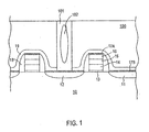
- Fig. 1 A W plug voiding problem addressed by the present invention is illustrated in Fig. 1 wherein transistors are formed on substrate 10.
- the transistors can comprise MOS transistors and/or dual gate memory cell transistors comprising floating and control gates with an interpoly (ONO) dielectric layer therebetween.
- the transistors can comprise a tunnel oxide 13, a floating gate electrode 14, an ONO stack interpoly dielectric 15, and a control gate 16.
- a layer of metal silicide 17A is formed on the upper surface of the gate electrode stack, while a layer of metal silicide 17B is formed on the source/drain regions 11, 12.
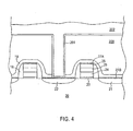
- transistors are formed on substrate 20.
- the transistor can comprise MOS transistors and/or dual gate memory cell transistors comprising floating and control gates with an interpoly (ONO) dielectric layer therebetween.
- the transistor can comprise a tunnel oxide 23, a floating gate electrode 24, and ONO stack interpoly dielectric 25 and a control gate 26.
- a layer of metal silicide 27A, e.g., nickel silicide, is formed on the upper surface of the gate electrode stack, while a layer metal silicide 27B, e.g., nickel silicide, is formed on the source/drain regions 21, 22.
- the contact opening typically has an aspect ratio (depth/diameter) of about 4:1 or greater.
- a composite barrier layer 201 is then deposited to line the opening, such as an initial layer of Ti and a layer of titanium nitride thereon. W is then deposited to fill the opening and form an overburden 202. Due to the high aspect ratio of the contact opening, significant voiding 203 is generated in the W plug.
- laser thermal annealing is conducted by impinging a pulsed laser light beam on the deposited W directed toward the filled contact, as schematically illustrated by arrows 30, typically at a radiant fluence of about 0.78 to about 1.10 joules/cm 2 , for a period of time of about 10 to about 100 nanoseconds, thereby elevating at a temperature of W in the plug to about 3,000°C to about 3,600°C, causing melting and reflowing to eliminate the voids, as schematically illustrated in Fig. 4.
- CMP is then conducted resulting in the structure illustrated in Fig. 5 wherein tungsten plug 50 does not exhibit voids.
- CMP is conducted prior to laser thermal annealing.
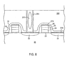
- Adverting to Fig. 6, the depicted structure is that resulting from performing CMP on the structure schematically illustrated in Fig. 2.
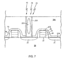
- Laser thermal annealing is then conducted, as illustrated in Fig. 7, by impinging a pulsed laser light beam 70 directed at the W plug causing reflowing and void elimination.
- the resulting structure is schematically illustrated in Fig. 8 and comprises W plug 80 without voids.
- the present invention provides methodology enabling the formation of interconnects having W contacts and/or vias with large aspect ratios, e.g., 4 or greater, with no or significantly reduced voids, thereby reducing contact resistance and stabilizing contact resistance distribution to provide a tighter resistance distribution, improving device reliability and improving electromigration performance.
- the present invention enjoys industrial applicability in manufacturing any of various types of semiconductor devices with improved reliability and increased circuit speed.
- the present invention has particular applicability in manufacturing semiconductor devices with design features in the deep sub-micron regime, such as flash memory devices, e.g., EEPROMs, with a design rule of about 0.12 micron and under, with significantly improved reliability, increased circuit speed, improved electromigration performance and improved manufacturing throughput.
Landscapes
- Engineering & Computer Science (AREA)
- Chemical & Material Sciences (AREA)
- Manufacturing & Machinery (AREA)
- Chemical Kinetics & Catalysis (AREA)
- Physics & Mathematics (AREA)
- Computer Hardware Design (AREA)
- Microelectronics & Electronic Packaging (AREA)
- Power Engineering (AREA)
- Condensed Matter Physics & Semiconductors (AREA)
- General Physics & Mathematics (AREA)
- Electrochemistry (AREA)
- Materials Engineering (AREA)
- Metallurgy (AREA)
- Organic Chemistry (AREA)
- Internal Circuitry In Semiconductor Integrated Circuit Devices (AREA)
- Semiconductor Memories (AREA)
- Non-Volatile Memory (AREA)
Applications Claiming Priority (3)
| Application Number | Priority Date | Filing Date | Title |
|---|---|---|---|
| US09/986,263 US6638861B1 (en) | 2001-11-08 | 2001-11-08 | Method of eliminating voids in W plugs |
| US986263 | 2001-11-08 | ||
| PCT/US2002/035910 WO2003040436A1 (en) | 2001-11-08 | 2002-11-08 | Method of eliminating voids in w plugs |
Publications (2)
| Publication Number | Publication Date |
|---|---|
| EP1442161A1 EP1442161A1 (en) | 2004-08-04 |
| EP1442161B1 true EP1442161B1 (en) | 2005-03-16 |
Family
ID=25532246
Family Applications (1)
| Application Number | Title | Priority Date | Filing Date |
|---|---|---|---|
| EP02802884A Expired - Lifetime EP1442161B1 (en) | 2001-11-08 | 2002-11-08 | Method of eliminating voids in w plugs |
Country Status (7)
Families Citing this family (18)
| Publication number | Priority date | Publication date | Assignee | Title |
|---|---|---|---|---|
| US7651910B2 (en) * | 2002-05-17 | 2010-01-26 | Micron Technology, Inc. | Methods of forming programmable memory devices |
| US6746944B1 (en) * | 2003-01-14 | 2004-06-08 | Advanced Micro Devices, Inc. | Low nisi/si interface contact resistance with preamorphizing and laser thermal annealing |
| GB0330010D0 (en) * | 2003-12-24 | 2004-01-28 | Cavendish Kinetics Ltd | Method for containing a device and a corresponding device |
| US7339230B2 (en) * | 2006-01-09 | 2008-03-04 | International Business Machines Corporation | Structure and method for making high density mosfet circuits with different height contact lines |
| US20070210448A1 (en) * | 2006-03-10 | 2007-09-13 | International Business Machines Corporation | Electroless cobalt-containing liner for middle-of-the-line (mol) applications |
| KR101477661B1 (ko) * | 2008-07-17 | 2014-12-31 | 삼성전자주식회사 | 텅스텐 재성장을 통한 심 없는 텅스텐 패턴 및 그 패턴형성 방법 |
| KR20100031962A (ko) * | 2008-09-17 | 2010-03-25 | 삼성전자주식회사 | 카본계막 식각 방법 및 이를 이용한 콘택홀 형성방법 |
| KR101534678B1 (ko) * | 2009-02-12 | 2015-07-08 | 삼성전자주식회사 | 텅스텐 콘택 플러그를 산소 분위기에서 rta 처리하고, rto 처리된 텅스텐 플러그를 수소 분위기에서 환원시키는 반도체 소자의 제조방법 |
| KR101525130B1 (ko) * | 2009-08-03 | 2015-06-03 | 에스케이하이닉스 주식회사 | 수직채널형 비휘발성 메모리 소자 및 그 제조 방법 |
| KR101858521B1 (ko) * | 2011-06-13 | 2018-06-28 | 삼성전자주식회사 | 비휘발성 메모리 장치의 제조 방법 |
| CN103311176B (zh) * | 2012-03-16 | 2015-04-29 | 中芯国际集成电路制造(上海)有限公司 | 金属连线的制作方法、半导体结构的制作方法 |
| KR102298605B1 (ko) | 2015-01-14 | 2021-09-06 | 삼성전자주식회사 | 수직형 메모리 장치 및 이의 제조 방법 |
| CN106128996A (zh) * | 2016-06-24 | 2016-11-16 | 武汉新芯集成电路制造有限公司 | 一种无缝多晶硅插塞的形成方法 |
| CN108987347B (zh) * | 2017-05-31 | 2020-10-09 | 联华电子股份有限公司 | 半导体结构的制作方法 |
| US10438846B2 (en) | 2017-11-28 | 2019-10-08 | Taiwan Semiconductor Manufacturing Co., Ltd. | Physical vapor deposition process for semiconductor interconnection structures |
| KR102208545B1 (ko) * | 2018-10-04 | 2021-01-28 | (주)알엔알랩 | 반도체 디바이스 제조 방법 |
| KR102840442B1 (ko) | 2020-07-29 | 2025-07-29 | 삼성전자주식회사 | 반도체 장치 및 이의 제조 방법 |
| CN118765110A (zh) * | 2023-03-27 | 2024-10-11 | 长鑫存储技术有限公司 | 半导体结构及其制造方法 |
Family Cites Families (7)
| Publication number | Priority date | Publication date | Assignee | Title |
|---|---|---|---|---|
| JPS61166143A (ja) * | 1985-01-18 | 1986-07-26 | Matsushita Electronics Corp | 半導体装置の製造方法 |
| US5780908A (en) * | 1995-05-09 | 1998-07-14 | Matsushita Electric Industrial Co., Ltd. | Semiconductor apparatus with tungstein nitride |
| US5885896A (en) * | 1996-07-08 | 1999-03-23 | Micron Technology, Inc. | Using implants to lower anneal temperatures |
| US6143650A (en) | 1999-01-13 | 2000-11-07 | Advanced Micro Devices, Inc. | Semiconductor interconnect interface processing by pulse laser anneal |
| EP1069213A3 (en) | 1999-07-12 | 2004-01-28 | Applied Materials, Inc. | Optimal anneal technology for micro-voiding control and self-annealing management of electroplated copper |
| US6399486B1 (en) | 1999-11-22 | 2002-06-04 | Taiwan Semiconductor Manufacturing Company | Method of improved copper gap fill |
| US6261963B1 (en) | 2000-07-07 | 2001-07-17 | Advanced Micro Devices, Inc. | Reverse electroplating of barrier metal layer to improve electromigration performance in copper interconnect devices |
-
2001
- 2001-11-08 US US09/986,263 patent/US6638861B1/en not_active Expired - Fee Related
-
2002
- 2002-11-08 CN CNA02821997XA patent/CN1582345A/zh active Pending
- 2002-11-08 JP JP2003542676A patent/JP2005508573A/ja active Pending
- 2002-11-08 DE DE60203319T patent/DE60203319T2/de not_active Expired - Lifetime
- 2002-11-08 WO PCT/US2002/035910 patent/WO2003040436A1/en active IP Right Grant
- 2002-11-08 EP EP02802884A patent/EP1442161B1/en not_active Expired - Lifetime
- 2002-11-08 KR KR1020047007012A patent/KR100892401B1/ko not_active Expired - Fee Related
Also Published As
| Publication number | Publication date |
|---|---|
| WO2003040436A1 (en) | 2003-05-15 |
| KR100892401B1 (ko) | 2009-04-10 |
| KR20050044376A (ko) | 2005-05-12 |
| EP1442161A1 (en) | 2004-08-04 |
| CN1582345A (zh) | 2005-02-16 |
| DE60203319D1 (de) | 2005-04-21 |
| DE60203319T2 (de) | 2006-03-16 |
| JP2005508573A (ja) | 2005-03-31 |
| US6638861B1 (en) | 2003-10-28 |
Similar Documents
| Publication | Publication Date | Title |
|---|---|---|
| EP1442161B1 (en) | Method of eliminating voids in w plugs | |
| US6686247B1 (en) | Self-aligned contacts to gates | |
| US6706576B1 (en) | Laser thermal annealing of silicon nitride for increased density and etch selectivity | |
| KR100555010B1 (ko) | 메모리와 로직 회로가 1칩에 혼재된 반도체 장치와 그제조 방법 | |
| JP4477349B2 (ja) | Nandフラッシュメモリ素子の製造方法 | |
| KR100860133B1 (ko) | 이온 주입에 의한 측벽 밀도의 국부적 증가 | |
| US7087524B2 (en) | Method of forming copper wiring in semiconductor device | |
| US20050285269A1 (en) | Substantially void free interconnect formation | |
| US20050140012A1 (en) | Method for forming copper wiring of semiconductor device | |
| US6900121B1 (en) | Laser thermal annealing to eliminate oxide voiding | |
| KR100524965B1 (ko) | 금속 플러그의 산화를 방지할 수 있는 캐패시터 및 그제조방법 | |
| KR100852207B1 (ko) | 절연막 제거방법 및 금속 배선 형성방법 | |
| US20040038526A1 (en) | Thermal process for reducing copper via distortion and crack | |
| KR100434187B1 (ko) | 반도체 장치의 절연막 패턴 형성 방법 | |
| JPH09153546A (ja) | 半導体装置及びその製造方法 | |
| KR101021176B1 (ko) | 반도체 소자의 금속배선 형성방법 | |
| JP2003124311A (ja) | 半導体装置の製造方法および半導体装置 | |
| KR100935193B1 (ko) | 반도체 소자의 금속배선 및 그의 형성방법 | |
| JP5191628B2 (ja) | 半導体装置構造および半導体装置の製造方法 | |
| JP2000164704A (ja) | 半導体装置及びその製造方法 | |
| KR100670686B1 (ko) | 반도체 소자의 콘택플러그 제조 방법 | |
| JP2006319116A (ja) | 半導体装置およびその製造方法 | |
| KR100519645B1 (ko) | 반도체 소자의 게이트 전극 형성방법 | |
| KR20110001586A (ko) | 반도체 소자의 패턴 형성방법 | |
| KR20100001653A (ko) | 반도체 소자의 콘택 플러그 형성 방법 |
Legal Events
| Date | Code | Title | Description |
|---|---|---|---|
| PUAI | Public reference made under article 153(3) epc to a published international application that has entered the european phase |
Free format text: ORIGINAL CODE: 0009012 |
|
| 17P | Request for examination filed |
Effective date: 20040421 |
|
| AK | Designated contracting states |
Kind code of ref document: A1 Designated state(s): AT BE BG CH CY CZ DE DK EE ES FI FR GB GR IE IT LI LU MC NL PT SE SK TR |
|
| AX | Request for extension of the european patent |
Extension state: AL LT LV MK RO SI |
|
| GRAP | Despatch of communication of intention to grant a patent |
Free format text: ORIGINAL CODE: EPIDOSNIGR1 |
|
| GRAP | Despatch of communication of intention to grant a patent |
Free format text: ORIGINAL CODE: EPIDOSNIGR1 |
|
| GRAS | Grant fee paid |
Free format text: ORIGINAL CODE: EPIDOSNIGR3 |
|
| GRAA | (expected) grant |
Free format text: ORIGINAL CODE: 0009210 |
|
| AK | Designated contracting states |
Kind code of ref document: B1 Designated state(s): DE GB |
|
| REG | Reference to a national code |
Ref country code: GB Ref legal event code: FG4D |
|
| REG | Reference to a national code |
Ref country code: IE Ref legal event code: FG4D |
|
| REF | Corresponds to: |
Ref document number: 60203319 Country of ref document: DE Date of ref document: 20050421 Kind code of ref document: P |
|
| PLBE | No opposition filed within time limit |
Free format text: ORIGINAL CODE: 0009261 |
|
| STAA | Information on the status of an ep patent application or granted ep patent |
Free format text: STATUS: NO OPPOSITION FILED WITHIN TIME LIMIT |
|
| 26N | No opposition filed |
Effective date: 20051219 |
|
| REG | Reference to a national code |
Ref country code: GB Ref legal event code: 732E Free format text: REGISTERED BETWEEN 20091210 AND 20091216 |
|
| PGFP | Annual fee paid to national office [announced via postgrant information from national office to epo] |
Ref country code: DE Payment date: 20101130 Year of fee payment: 9 |
|
| PGFP | Annual fee paid to national office [announced via postgrant information from national office to epo] |
Ref country code: GB Payment date: 20101022 Year of fee payment: 9 |
|
| GBPC | Gb: european patent ceased through non-payment of renewal fee |
Effective date: 20111108 |
|
| PG25 | Lapsed in a contracting state [announced via postgrant information from national office to epo] |
Ref country code: GB Free format text: LAPSE BECAUSE OF NON-PAYMENT OF DUE FEES Effective date: 20111108 |
|
| REG | Reference to a national code |
Ref country code: DE Ref legal event code: R119 Ref document number: 60203319 Country of ref document: DE Effective date: 20130601 |
|
| PG25 | Lapsed in a contracting state [announced via postgrant information from national office to epo] |
Ref country code: DE Free format text: LAPSE BECAUSE OF NON-PAYMENT OF DUE FEES Effective date: 20130601 |