EP1441446B1 - Réseau de cellules de courant - Google Patents
Réseau de cellules de courant Download PDFInfo
- Publication number
- EP1441446B1 EP1441446B1 EP04010234A EP04010234A EP1441446B1 EP 1441446 B1 EP1441446 B1 EP 1441446B1 EP 04010234 A EP04010234 A EP 04010234A EP 04010234 A EP04010234 A EP 04010234A EP 1441446 B1 EP1441446 B1 EP 1441446B1
- Authority
- EP
- European Patent Office
- Prior art keywords
- cell
- cell array
- cells
- array
- circuitry
- Prior art date
- Legal status (The legal status is an assumption and is not a legal conclusion. Google has not performed a legal analysis and makes no representation as to the accuracy of the status listed.)
- Expired - Lifetime
Links
Images


Classifications
-
- H—ELECTRICITY
- H03—ELECTRONIC CIRCUITRY
- H03M—CODING; DECODING; CODE CONVERSION IN GENERAL
- H03M1/00—Analogue/digital conversion; Digital/analogue conversion
- H03M1/06—Continuously compensating for, or preventing, undesired influence of physical parameters
- H03M1/0617—Continuously compensating for, or preventing, undesired influence of physical parameters characterised by the use of methods or means not specific to a particular type of detrimental influence
- H03M1/0634—Continuously compensating for, or preventing, undesired influence of physical parameters characterised by the use of methods or means not specific to a particular type of detrimental influence by averaging out the errors, e.g. using sliding scale
- H03M1/0643—Continuously compensating for, or preventing, undesired influence of physical parameters characterised by the use of methods or means not specific to a particular type of detrimental influence by averaging out the errors, e.g. using sliding scale in the spatial domain
- H03M1/0651—Continuously compensating for, or preventing, undesired influence of physical parameters characterised by the use of methods or means not specific to a particular type of detrimental influence by averaging out the errors, e.g. using sliding scale in the spatial domain by selecting the quantisation value generators in a non-sequential order, e.g. symmetrical
-
- H—ELECTRICITY
- H03—ELECTRONIC CIRCUITRY
- H03M—CODING; DECODING; CODE CONVERSION IN GENERAL
- H03M1/00—Analogue/digital conversion; Digital/analogue conversion
- H03M1/06—Continuously compensating for, or preventing, undesired influence of physical parameters
- H03M1/0617—Continuously compensating for, or preventing, undesired influence of physical parameters characterised by the use of methods or means not specific to a particular type of detrimental influence
- H03M1/0634—Continuously compensating for, or preventing, undesired influence of physical parameters characterised by the use of methods or means not specific to a particular type of detrimental influence by averaging out the errors, e.g. using sliding scale
- H03M1/0643—Continuously compensating for, or preventing, undesired influence of physical parameters characterised by the use of methods or means not specific to a particular type of detrimental influence by averaging out the errors, e.g. using sliding scale in the spatial domain
- H03M1/0648—Continuously compensating for, or preventing, undesired influence of physical parameters characterised by the use of methods or means not specific to a particular type of detrimental influence by averaging out the errors, e.g. using sliding scale in the spatial domain by arranging the quantisation value generators in a non-sequential pattern layout, e.g. symmetrical
-
- H—ELECTRICITY
- H03—ELECTRONIC CIRCUITRY
- H03M—CODING; DECODING; CODE CONVERSION IN GENERAL
- H03M1/00—Analogue/digital conversion; Digital/analogue conversion
- H03M1/66—Digital/analogue converters
- H03M1/74—Simultaneous conversion
- H03M1/742—Simultaneous conversion using current sources as quantisation value generators
- H03M1/747—Simultaneous conversion using current sources as quantisation value generators with equal currents which are switched by unary decoded digital signals
Definitions
- the present invention relates to cell array circuitry for use, for example, in digital-to-analog converters (DACs) .
- DACs digital-to-analog converters
- FIG. 1 of the accompanying drawings shows parts of a conventional digital-to-analog converter (DAC) of the so-called "current-steering" type.
- the DAC 1 is designed to convert an m-bit digital input word (D1-Dm) into a corresponding analog output signal.
- the DAC 1 further includes a plurality of differential switching circuits 4 1 to 4 n corresponding respectively to the n current sources 2 1 to 2 n . Each differential switching circuit 4 is connected to its corresponding current source 2 and switches the current I produced by the current source either to a first terminal, connected to a first connection line A of the converter, or a second terminal connected to a second connection line B of the converter.
- Each differential switching circuit 4 receives one of a plurality of control signals T1 to Tn (called “thermometer-coded signals” for reasons explained hereinafter) and selects either its first terminal or its second terminal in accordance with the value of the signal concerned.
- a first output current I A of the DAC 1 is the sum of the respective currents delivered to the differential-switching-circuit first terminals
- a second output current I B of the DAC 1 is the sum of the respective currents delivered to the differential-switching-circuit second terminals.
- the analog output signal is the voltage difference V A- V B between a voltage V A produced by sinking the first output current I A of the DAC 1 into a resistance R and a voltage V B produced by sinking the second output current I B of the converter into another resistance R.
- thermometer-coded signals T1 to Tn are derived from the binary input word D1-Dm by a binary-thermometer decoder 6.
- the decoder 6 operates as follows.
- thermometer-coded signals T1-Tn are such that each of the differential switching circuits 4 1 to 4 n selects its second terminal so that all of the current sources 2 1 to 2 n are connected to the second connection line B.
- the analog output signal V A -V B -nIR.
- thermometer-coded signals T1 to Tn produced by the decoder 6 are such that more of the differential switching circuits select their respective first terminals (starting from the differential switching circuit 4 1 ) without any differential switching circuit that has already selected its first terminal switching back to its second terminal.
- the first i differential switching circuits 4 1 to 4 i select their respective first terminals, whereas the remaining n-i differential switching circuits 4 i+1 to 4 n select their respective second terminals.
- the analog output signal V A -V B is equal to (2i-n)IR.
- thermometer-coded signals T1 to Tn generated by the binary-thermometer decoder 6 follow a so-called thermometer code in which it is known that when an rth-order signal Tr is activated (set to "1"), all of the lower-order signals T1 to Tr-1 will also be activated.
- Thermometer coding is popular in DACs of the current-steering type because, as the binary input word increases, more current sources are switched to the first connection line A without any current source that is already switched to that line A being switched to the other line B. Accordingly, the input/output characteristic of the DAC is monotonic and the glitch impulse resulting from a change of 1 in the input word is small.
- each cell CL ij is arranged in an 8 x 8 square array having eight rows and eight columns.
- the first digit of the suffix applied to each cell denotes the row in which the cell is located and the second digit of the suffix denotes the column in which the cell is located.
- the cell CL 18 is the cell in row 1, column 8.
- Each cell CL ij includes its own current source 2 and its own differential switching circuit 4.
- the respective first terminals of the cells of the array are connected together to a first connection line A of the DAC and the respective second terminals of the cells of the array are connected together to a second connection line B of the DAC, as in the Figure 1 DAC.
- thermometer-coded signals In order to avoid having to generate and supply different respective thermometer-coded signals to all the cells of the array, a two-stage decoding process is adopted to convert the binary input word D1-D6 into the respective thermometer-coded control signals T required by the differential switching circuits 4 in the different cells.
- the first stage of this two-stage decoding process is carried out by respective row and column decoders 12 and 14, and the second stage is carried out by a local decoder 16 provided for each cell.
- the three lower-order bits D1-D3 of the binary input word are applied to the column decoder 14 which derives therefrom seven thermometer-coded column selection signals in accordance with Figure 2.
- the row decoder 12 receives the three higher-order bits D4-D6 of the input word and derives therefrom seven thermometer-coded row selection signals, also in accordance with Figure 2.
- the row and column selection signals are distributed to the cells of the array.
- each cell the local decoder 16 combines the row and column selection signals to derive therefrom the required local control signal T for the differential switching circuit 4 of the cell concerned.
- the local decoder 16 in each cell does not need to employ all seven row and column selection signals to produce the required local control signal T. This is because, for any digital input word, the rows of the matrix fall into one of three different states: (1) rows in which the respective differential switching circuits of all cells of the row select the second terminal; (2) rows in which the respective differential switching circuits of all cells of the row select the first terminal; and (3) a (unique) row in which the differential switching circuits of one or more cells of the row select the second terminal whereas the differential switching circuits of one or more other cells of the row select the first terminal. In view of these limited possibilities, it is possible for each local decoder to derive its local control signal T simply by combining two of the row selection signals r n and r n+1 and one of the column selection signals c n .
- the numbers allotted to the cells CL ij in Figure 3 denote the sequence in which the cells are activated (or controlled) to change from selecting their respective second terminals to selecting their respective first terminals.
- the activation sequence follows the physical order of the cells in the array, starting from row 1 and activating the cells of that row sequentially in column order, followed by row 2, and so on for each successive row of the array.
- a voltage drop along a power supply line can cause a graded error along a row or column, as shown in Figure 4(A).
- the current sources in the first four cells of the row or column concerned may have negative errors, signifying that each of them produces a below-average output current. These negative errors decrease towards the centre of the row or column concerned.
- the current sources in the remaining cells 5 to 8 of the row or column concerned have respective positive errors, signifying that each of them produces an above-average output current. These positive errors increase from the centre of the row or column to the end.
- Thermal distribution inside a chip including the array can cause a symmetrical error within a row or column, as shown in Figure 4(B).
- the current sources in the end cells 1, 2, 7 and 8 of the row or column have negative errors
- the current sources of the central cells 3 to 6 of the row or column have positive errors.
- the final error distribution for the cell array is produced by superposing all the different error components.
- the graded and symmetrical errors shown in Figures 4(A) and Figure 4(B) tend to accumulate and result in a large integral linearity error (INL).
- INL integral linearity error
- the graded error distribution shown in Figure 4(A) exists within the first row of the cell array shown in Figure 3.
- the negative errors accumulate, amounting to a significant total negative error when the digital input code is 4. Only when cells 5 to 8 are sequentially activated do the positive errors attributable to these cells start to cancel out the large negative error attributable to cells 1 to 4.
- US 4812818 discloses cell array circuitry which may be considered to include: respective first and second cell arrays, each cell array being made up of a plurality of mutually-corresponding cells arranged in rows and columns, the second cell array being placed in a predetermined spatial relationship with respect to the first cell array; cell set selection means for selecting the cells of the arrays in sets, each such cell set including a first cell from the first cell array and an individually-corresponding second cell from the second cell array, the physical arrangement of such second cells within the second cell array corresponding to a predetermined transformation of the physical arrangement of their respective corresponding first cells within the first cell array; and accumulation means for accumulating respective analog quantities produced by, or associated with, the first and second cells of a selected cell set.
- the different rows in the first and second array are activated in a particular pattern to minimise second order errors resulting from stresses in the integrated circuit chip.
- the second array has its cells in a reverse-image arrangement to the cells of the first array to minimise differential non-linearities on the chip.
- EP-A-0399456 discloses a digital-to-analog converter having a plurality of segment groups. Each segment group is made up of a number of individual segments. The segments within a segment group are selected and respective analog quantities (e.g. currents) of the selected segments are accumulated. The segments of different segment groups are intermingled in a two-dimensional arrangement so that the positions of the centres of gravity of the respective segment groups are substantially matched with the centre of the arranged segments.
- Cell array circuitry embodying the present invention is characterised by: respective third and fourth such cell arrays, each made up of a plurality of mutually-corresponding cells arranged in rows and columns and each placed in a predetermined spatial relationship with respect to the first cell array; and in that: each said cell set selected by the cell set selection means further includes a third cell from the third cell array, which third cell corresponds individually to the first cell of the cell set concerned, and a fourth cell from the fourth cell array, which fourth cell corresponds individually to the first cell of the cell set concerned; the physical arrangement of such third cells within the third cell array corresponds to a predetermined transformation of the physical arrangement of their respective corresponding first cells within the first cell array, and the physical arrangement of such fourth cells within the fourth cell array corresponds to a predetermined transformation of the physical arrangement of their respective corresponding first cells within the first cell array; and the accumulation means are operable to accumulate respective analog quantities produced by, or associated with, the first, second, third and fourth cells of a selected cell set.
- an area containing the four cell arrays may be considered to be divided into four quadrants by respective first and second mutually-perpendicular axes that intersect at an origin point of the area, the first, second, third and fourth cell arrays being arranged respectively in the four quadrants.
- the second, third and fourth cell arrays could simply be copies of the first cell array, which would enable symmetrical errors parallel to both axes to be cancelled.
- first and second ones of the quadrants are on the same side of the said second axis, and the said first quadrant and a third one of the quadrants are on the same side of the first axis;
- the first cell array is located in the said first quadrant;
- the second cell array corresponds to a reflection about the said second axis of the said first cell array, which reflection is located in the said second quadrant;
- the third cell array corresponds to a reflection about the said first axis of the said first cell array, which reflection is located in the said third quadrant;
- the fourth cell array corresponds to a rotation through 180° of the said first cell array, which rotation is located in the said fourth quadrant.
- the result of arranging the first, second, third and fourth cell arrays in such a configuration is that the corresponding cells of each cell set have a common centroid at the origin. In this case, both graded and symmetrical errors parallel to both axes are cancelled: a highly-desirable effect.
- the cells may include any suitable type of analog circuitry where matching between respective analog quantities produced by, or associated with, the different cells is required.
- each cell may include a current source or current sink circuit, in which case the accumulation means may be operable to accumulate respective currents sourced, or sunk as the case may be, by the current source/sink circuits of the selected cells.
- each cell may include a capacitance element, in which case the accumulation means may be operable to accumulate respective charges stored by the capacitance elements of the selected cells.
- each cell may include a resistance element, in which case the accumulation means may be operable to accumulate respective resistances of the resistance elements of the selected cells.
- the selection means may, for example, be operable to select together each cell of the array whose said assigned ordinal position is less than a given value. For example, when the given value is i, the cells whose assigned ordinal positions are 1,2,...,i-1 are selected. It is convenient in this case if the said given value is determined by a selection signal (a digital input word) applied to the said selection means.
- the selection means could alternatively be operable to select the cells of the array in at least first and second binary-weighted groups, the number of cells in the first group being double the number of cells in the second group.
- This type of selection is suitable for use in a "charge distribution" ADC which requires binary-weighted capacitors.
- These binary-weighted capacitors can be formed by selecting binary-ratioed numbers (e.g. 1,2,4,8...) of capacitor-cells from the cell array and connecting the selected cells in parallel with one another.
- the cells in the group have consecutive assigned ordinal positions. This helps to ensure that, within each group containing two or more cells, errors are cancelled.
- the cell set selection means may serve to assign the cells of each cell array respective ordinal positions in a predetermined selection sequence and to select the cells in accordance with their respective assigned ordinal positions, and the said accumulation means may be operable to accumulate respective analog quantities (e.g. currents, capacitances, resistances etc.) produced by, or associated with, the cells of the selected cell sets.
- respective analog quantities e.g. currents, capacitances, resistances etc.
- the assigned ordinal positions may simply conform to the physical order of the cells in the cell array concerned.
- the assigned ordinal positions may be such as to tend to equalise the respective sequence-position sums for different rows of the array and/or to tend to equalise the respective sequence-position sums for different columns of the array, where the sequence-position sum for a row or column is determined by summing the respective ordinal positions of the cells in the row or column concerned.
- the assigned ordinal positions are preferably such as to tend to equalise the respective sequence-position sums for just some of the rows of the array and/or to tend to equalise the respective sequence-position sums for just some of the columns of the array. It is certainly not essential for every row to have the same sequence-position sum or for every column to have the same sequence-position sum.
- the assigned ordinal positions are such as to tend to equalise the respective sequence-position sums for all the rows of the array and/or to tend to equalise the respective sequence-position sums for all the columns of the array. This increases the effectiveness in overcoming the errors associated with the different cells.
- the said assigned ordinal positions are such as to tend to equalise the respective sequence-position sums for all rows and columns of the array. This can be achieved, for example, by distributing the said assigned ordinal positions within the array such that they conform to the distribution of integers in a magic square of order equal to the number of rows or columns of the array.
- the magic square may be pandiagonal and/or associative. This may give additional error-compensating effects depending on the mode of selection of the cells.
- the cell array is rectangular (i.e. has different numbers of rows and columns)
- the sequence-position sum(s) for the rows it is not necessary for the sequence-position sum(s) for the rows to be the same as the sequence-position sum(s) for the columns.
- the said assigned ordinal positions are preferably such as to tend to equalise the respective sequence-position sums for all rows and to tend to equalise the respective sequence-position sums for all columns.
- Figure 5 shows parts of cell array circuitry.
- the Figure 5 circuitry does not directly embody the present invention but an understanding of the Figure 5 circuitry may be helpful for understanding embodiments of the present invention described later with reference to Figures 19 to 23.
- the Figure 5 cell array circuitry 20 is suitable for use in a digital-to-analog converter of the current-steering type.
- components which correspond to components already described with reference to the DAC of Figure 3 have the same reference numerals as used in Figure 3.
- the cell array circuitry 20 comprises a cell array 22 made up of 16 individual cells arrayed in four rows and four columns. Each cell comprises a current source 2, as shown schematically for the cell numbered 11 in Figure 5. Each cell has an output node denoted by a cross within the cell in Figure 5.
- Each cell of the cell array 22 has an individually-corresponding switch circuit 4 1 to 4 16 .
- the switch circuits 4 are external to the cells and the output node of each cell is connected to an input node of its individually-corresponding switch circuit 4.
- Each switch circuit has respective first and second terminals, the first terminal being connected to a first summing connection line A and the second terminal being connected to a second summing connection line B.
- the switch circuits 4 1 to 4 16 receive respective thermometer-coded selection signals S1 to S16 from decoding circuitry of the DAC (not shown).
- This decoding circuitry may derive the selection signals S1 to S16 directly (in one stage) from a binary input word of the DAC (as shown schematically in Figure 1) or in two stages using respective row and column decoders to perform the first stage of the decoding and using local decoders corresponding respectively to the cells to perform the second stage of the decoding (as shown in Fig. 3).
- Each switch circuit selects its second output terminal when the selection signals applied to it has the low logic level L and selects its first output terminal when the selection signal S applied to it has the high logic level H.
- the selection signals S1 and S2 are both H, whereas the remaining selection signals S3 to S16 are L.
- the switch circuits 4 1 and 4 2 have selected their respective first terminals, whereas the remaining switch circuits are selecting their respective second terminals.
- the cells in the cell array 22 of Figure 5 are selected in a sequence different from the conventional selection sequence described above with reference to Figure 3.
- the selection sequence in this example is such that, for each row, column and diagonal of the cell array 22, the sum of the respective selection-sequence positions of the cells is the same (in this case 34).
- the respective selection-sequence positions 1, 15, 14 and 4 add up to 34.
- the respective selection-sequence positions 1, 12, 8 and 13 of the cells of column 1 also add up to 34.
- the respective selection-sequence positions of the cells are 1, 6, 11 and 16 which again add up to 34.
- the table shows the x-error and y-error for each ordinal position in the selection sequence of the cells.
- the respective x-errors sum to produce a total x-error ⁇ x
- the respective y-errors sum to produce a total y-error ⁇ y.
- the total x-error ⁇ x varies in a small range from -2 to +2, as does the total y-error ⁇ y.
- the total error E (which the sum of the total x-error ⁇ x and the total y-error ⁇ y) varies within a narrow range from -4 to +3.
- Figure 7(A) shows the error values and accumulations in the case in which the selection sequence in the cell array is as shown in Figure 7(B).
- the total x-error Ex, the total y-error ⁇ y and the total error E each vary in greater ranges than the corresponding total errors in Figure 6.
- the total y-error ⁇ y is consistently negative and reaches -12 in the worst case.
- the total x-error Ex although relatively small compared to the total y-error ⁇ y, is also consistently negative and so has the effect of increasing the total error E for every input code.
- Figure 9(A) shows, as a starting point, the magic square of Figure 8.
- Figure 9(B) shows the effect of rotating the magic square of Figure 9(A) anticlockwise through 90°, as denoted by the arrow labelled B in Figure 9(A).
- Figures 9(C) and (D) relate respectively to anticlockwise rotations of 180 and 270°, as denoted by the arrows C and D in Figure 9(A).
- Figures 9(E) to (H) show the effect of reflecting the magic square of Figure 9(A) about various axes E to H. Further magic squares can be obtained by using combinations of the basic rotations and reflections shown in Figures 9(B) to 9(H).
- a fourth-order square i.e. four rows and four columns
- the numbers in each of the rows, columns and diagonals of the fourth-order square add up to 34.
- a fifth-order square has 275,305,224 different placings, excluding rotations and reflections.
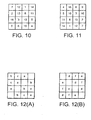
- Figures 10 and 11 show two alternative possibilities, each different from the arrangement shown in Figure 5.
- any pair of numbers opposite the centre adds up to n 2 +1 (the order n being 5 in this case).
- Such a magic square is called "associative".
- the third-order magic square shown in Figure 8 also has this property and is therefore associative.
- a fourth-order square may be either associative or pandiagonal but not both.
- the smallest square that can be both associative and pandiagonal is of the fifth order.
- Embodiments of the present invention can be constructed such that the selection sequence within the cell array is in accordance with any suitable magic square of the appropriate order, whether or not the square is pandiagonal and/or associative.
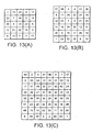
- Figure 14(B) shows a rectangular array having 2 rows and 3 columns.
- the sums for columns 1 to 3 have the same value 7 whereas the sums for rows 1 and 2 are as close as possible, at 10 and 11 respectively.
- the columns have less cells than the rows in this case, it is not possible to equalise the sums for rows and columns. Instead, it is sufficient to seek to minimise the deviation between the different rows (in this case 1) and to minimise the deviation between the different columns (in this case 0).
- each cell is constituted by a current source 2.
- the current source 2 comprises a PMOS field-effect transistor 32 having its source connected to a positive power supply line Vdd, its gate connected to receive a predetermined bias potential Vbias and its drain connected to an output node OUT of the current source.
- the predetermined bias potential Vbias has a constant potential difference from the positive power supply potential Vdd, for example. Accordingly, the transistor 32 is permanently turned on and supplies a substantially constant current I to its output node OUT.
- each cell 2 in Figure 5 could comprise a current sink circuit in place of the current source circuit 2.
- the transistor 32 shown in Figure 15 is changed to an NMOS FET and the source of the transistor is connected to a negative supply line potential such as Vss.
- Vbias is a predetermined reference potential above Vss, for example having a constant potential difference from Vss.
- either the current source or the current sink can be implemented by using bipolar transistors.
- respective capacitance elements C are included in the different cells 44 of a cell array 42.
- Each cell 44 has an individually-corresponding switch circuit 46 1 to 46 16 .
- An input node of each switch circuit 46 is connected to an output node (denoted by a cross in Figure 16) of its corresponding cell 44. This output node is connected to a bottom plate of the capacitance element C in the cell.
- each switch circuit has three terminals, the respective first terminals being connected in common to receive an input voltage V IN , the respective second terminals being connected in common to a negative reference voltage Vss, and the respective third terminals being connected in common to receive a predetermined reference potential V REF .
- Each switch circuit 46 is controllable, in dependence upon a selection signal S applied thereto, to connect its input node to one of its first, second and third terminals.
- the respective top plates of the capacitance elements C in the different cells are connected in common to a first input of a comparator 48. This first input is also connected via a switch element 50 to Vss. A second input of the comparator 48 is connected to Vss. A digital output signal D is produced at the output of the comparator 48.
- the cell array circuitry shown in Figure 16 is suitable for use in a successive-approximation analog-to-digital converter (ADC) which operates in accordance with the so-called "charge redistribution" principle.
- ADC analog-to-digital converter
- Such a successive-approximation ADC employs a digital-to-analog converter (DAC) incorporating binary-weighted capacitors. Further information on this type of capacitor DAC can be found, for example, in IEEE Journal of Solid State Circuits, Vo. Sc-14, pp.920-926, December 1979.
- capacitors C 0 to C 4 are provided by the capacitance elements C in the different cells, as shown in the top right-hand corner of Figure 16.
- the capacitor C 0 is provided by the capacitance element C of cell 1 alone.
- the capacitor C 1 is provided by the capacitance element C of cell 2 alone.
- the capacitor C 2 is provided by the respective capacitance elements C of cells 3 and 4 connected in parallel.
- the capacitor C 3 is provided by the respective capacitance elements C of cells 5 to 8 connected in parallel.
- the capacitor C 4 is provided by the respective capacitance elements C of cells 9 to 16 connected in parallel.
- the capacitance ratios of the capacitors C 0 to C 4 are therefore 1: 1: 2: 4: 8.
- the cell array circuitry 40 in Figure 16 operates as follows. Firstly, in a sampling mode of the circuitry, the top plates of all of the capacitors C 0 to C 4 are connected to Vss using the switch element 50, and all the bottom plates are connected to receive the input voltage V IN by controlling the switch circuits 46 1 to 46 16 so that all of them select their respective first terminals.
- the analog-to-digital conversion process then commences. In this process it is identified which of the capacitors C 1 to C 4 need to have their bottom plates changed from Vss potential to V REF potential in order for the top plate voltage V TOP to become 0. This determination is made according to a binary search algorithm.
- the bottom plate of C 4 is switched from Vss to V REF so that the top plate voltage V TOP increases by an amount equal to 1 ⁇ 2 V REF .
- This is accomplished by causing the switch circuits 46 9 to 46 16 , corresponding to cells 9 to 16 whose respective capacitance elements make up the capacitor C 4 , to operate in parallel to change their selections from the second terminal (connected to Vss) to the third terminal (connected to V REF ).
- the output D of the comparator 48 indicates the polarity of the difference between the top plate voltage V TOP and V SS , which in turn determines the value of the most significant bit of the digital output word.
- the remaining bits of the digital output word are determined iteratively in a similar manner.
- Figure 17 shows yet another example in which cell array circuitry 60 includes a cell array 62 made up of individual cells 64, each containing a resistance element R.
- a bus 70 is used to make connections between the different cells 64 and a selector circuit 72.
- the selector circuit 72 has inputs I 1 to I 17 connected to respective bus lines 70 1 to 70 17 of the bus 70.
- the first and last bus lines 70 1 and 70 17 are connected respectively to nodes N 1 and N 2 of the cell array circuitry.
- the resistance element R of each cell 64 is connected in series, via connection lines 66 and 68, between a pair of mutually-adjacent bus lines.
- the resistance element R of cell 1 is connected in series between the bus lines 70 1 and 70 2 .
- the selector circuit 72 is selectively controllable, in accordance with a digital selection word S applied thereto, to make a connection between one of its inputs I 1 to I 17 and an output O thereof which is connected to an output node OUT of the cell array circuitry 60.
- the selector circuit 72 connects its input I 3 to its output O
- the number of resistance elements R connected in series between the first node N 1 of the circuitry and the output node OUT of the circuitry is two (the resistance elements in cells 1 and 2)
- the number of resistance elements connected between the nodes N 2 and OUT is 14 (the resistance elements in cells 3 to 16 inclusive).
- the cell array circuitry in this example functions as a digitally-controllable potentiometer, the position of the output tap being determined by the value of the digital selection word S.
- the nodes N 1 and N 2 may be connected to first and second power supply lines Vdd and V SS respectively.
- a constant-current generator may be interposed between, on the one hand, one of the nodes N 1 and N 2 , and, on the other hand, the power supply line to which the node is connected.
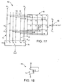
- the resistance element R in each cell in Figure 11 can be formed, for example, by a depletion-type MOSFET 74 as shown in Figure 18. Several such transistors can be connected in parallel if higher current capacity is required.
- the quantities being summed as the cells are selected sequentially are currents.
- the quantities being summed are charges.
- the quantities being summed are resistances.
- the present invention is not restricted to summing these three quantities. Any suitable analog quantities can be summed in cell array circuitry embodying the present invention.
- the invention is applicable advantageously in any situation in which respective analog quantities produced by, or associated with, nominally-matched cells must be accumulated or summed in some way.
- the cells may incorporate their respective associated switch circuits as well as parts of any decoding circuitry, if desired.
- the switch circuits and decoding circuitry it is normally preferable for the switch circuits and decoding circuitry to be external to the cells.
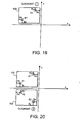
- a first cell array 100 made up of a plurality of individual cells arrayed in rows and columns, is placed in a first quadrant.
- Two representative cells A1 and B1 of the array 100 are shown in Figure 19, the cell A1 being spaced by distances Ax and Ay from the nearest edges in the x and y directions respectively, and the cell B1 being spaced from its nearest edges by distances Bx and By in the x and y directions respectively.
- a second cell array 102 is placed in a second quadrant.
- the arrangement of cells in the second cell array 102 is produced by reflecting the first cell array 100 about the y axis and then translating (moving) the resulting reflection into the second quadrant.
- representative cells A2 and B2 of the second cell array 102 which correspond respectively to the representative cells A1 and B1 of the first cell array 100, are located as shown in Figure 20.
- a third cell array 104 is placed in a third quadrant.
- the arrangement of cells in the third cell array 104 is produced by reflecting the first cell array 100 about the x axis and then shifting the resulting reflection into the third quadrant.
- Representative cells A3 and B3, corresponding respectively to the representative cells A1 and B1 of the cell array 100, are shown in Figure 21.
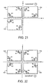
- a fourth cell array 106 is placed in a fourth quadrant.
- the arrangement of the cells in the fourth cell array 106 is produced by rotating the first cell array 100 through 180° about the origin.
- Representative cells A4 and B4, corresponding respectively to the representative cells A1 and B1 of the first cell array 100, are shown in Figure 22.
- the result of arranging the first, second, third and fourth cell arrays 100 to 106 in the configuration shown in Figure 22 is that the corresponding representative cells of the four cell arrays have a common centroid at the origin.
- A1 and A4 are both spaced by the same distance Ax from the y axis on opposite sides thereof, and the cells A2 and A3 are also equidistant from the y axis on opposite sides thereof.
- A1 and A4 are equidistant from the x axis on opposite sides thereof, as are the cells A2 and A3.
- any graded errors in the x-direction attributable to A1 and A4 cancel one another out.
- Any graded x-direction errors attributable to A2 and A3 also cancel one another out. The same is true for y-direction graded errors.
- A1 is spaced from the top edge of the area occupied by the four cell arrays 100-106 by the same distance Ay as A2 is spaced from the centreline of the area in the y-direction (that is from the x axis). Any symmetrical y-direction errors attributable to A1 and A2 therefore cancel one another out. The same is true for A3 and A4 in the y-direction, and for A1 and A3 and for A2 and A4 in the x-direction.
- the selection sequence of the cells within the first cell array 100 (which in turn determines the respective selection sequences within the other cell arrays 102, 104 and 106 derived from the first cell array 100) is not critical. For example, it would be possible simply to select the cells in a conventional selection sequence as shown in Figure 3 (i.e. columns of row 1, followed by columns of row 2, and so on). However, preferably, the selection sequence within the first cell array 100 is determined in accordance with the principles described previously with reference to Figures 5 to 14(B). In this case, graded, symmetrical and other errors within each individual cell array can be compensated as well as the errors present across the area occupied by the four cell arrays as a whole.
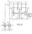
- Figure 23 shows an example of the way in which the four different cells belonging to each set of cells can be connected together and selected.
- each set of four corresponding cells has an individually-corresponding switch circuit 4.
- the set of four cells A1 to A4 has an individually-corresponding switch circuit 4 A .
- the cells are constituted by respective constant-current sources 2 and the four cells of a set are connected to a common connection line 110 that is connected to an input of the corresponding switch circuit.
- each cell may be constituted by a single transistor or by plural transistors connected in parallel.
- each cell may comprise four parallel-connected p-type FETs.
- the cells in the four cell arrays of Figure 23 need not comprise constant-current sources. They could alternatively comprise constant-current sink circuits. Furthermore, they could comprise capacitance elements C as shown in Figure 16, or resistance elements R as shown in Figure 17. In this case, the connections from the cells to the switch circuits should be modified in accordance with Figures 16 and 17, as appropriate.
- Another possibility is to place four identical cell arrays 100 in quadrants 1 to 4 respectively. This has the effect of cancelling out symmetrical errors in both the x-and y-directions.
- the cell arrays it is not necessary for the cell arrays to be placed directly adjacent to one another in embodiments of the present invention.
- the arrays 100 and 102 could be spaced apart in the x-direction from the arrays 104 and 106 so as to leave a space in which to place further circuitry such as other cells of the DAC.
Claims (19)
- Réseau de cellules comprenant :des première et seconde matrices de cellules respectives (100, 102), chaque matrice de cellules étant constituée d'une pluralité de cellules correspondant mutuellement (A1, B1, A2, B2) agencées en lignes et en colonnes, la seconde matrice de cellules (102) étant placée dans une relation spatiale prédéterminée par rapport à la première matrice de cellules (100),un moyen de sélection d'ensemble de cellules (4A, 4B) destiné à sélectionner les cellules des matrices en ensembles (A1+A2, B1+B2), chaque tel ensemble de cellules comprenant une première cellule de la première matrice de cellules (100) et une seconde cellule correspondant individuellement à la seconde matrice de cellules (102), l'agencement physique de telle secondes cellules (A2, B2) à l'intérieur de la seconde matrice de cellules (102) correspondant à une transformation prédéterminée de l'agencement physique de leurs premières cellules correspondantes respectives (A1, B1) à l'intérieur de la première matrice de cellules (100), etun moyen d'accumulation destiné à cumuler des quantités analogiques respectives produites par, ou associées avec, les première et seconde cellules d'un ensemble de cellules sélectionné,caractérisé par :des troisième et quatrième telles matrices de cellules respectives (104, 106), chacune constituée d'une pluralité de cellules correspondant mutuellement (A3, B3, A4, B4) agencées en lignes et colonnes et chacune est placée dans une relation spatiale prédéterminée par rapport à la première matrice de cellules (100),et en ce que :chaque dit ensemble de cellules sélectionné par le moyen de sélection d'ensemble de cellules (4A, 4B) comprend en outre une troisième cellule de la troisième matrice de cellules (104), laquelle troisième cellule correspond individuellement à la première cellule de l'ensemble de cellules concerné, et une quatrième cellule du quatrième ensemble de cellules (106), laquelle quatrième cellule correspond individuellement à la première cellule de l'ensemble de cellules concerné,l'agencement physique de telles troisièmes cellules (A3, B3) à l'intérieur de la troisième matrice de cellules correspond à une transformation prédéterminée de l'agencement physique de leurs premières cellules correspondantes respectives (A1, B1) à l'intérieur de la première matrice de cellules (100), et l'agencement physique de telles quatrièmes cellules (A4, B4) à l'intérieur de la quatrième matrice de cellules (106) correspond à une transformation prédéterminée de l'agencement physique de leurs premières cellules respectives correspondantes (A1, B1) à l'intérieur de la première matrice de cellules (100), etle moyen d'accumulation qui peut être mis en oeuvre pour accumuler des quantités analogiques respectives produites par, ou associées avec, les première, seconde, troisième et quatrième cellules (A1 à A4, B1 à B4) de l'ensemble de cellules sélectionné.
- Réseau de cellules selon la revendication 1, dans lequel une zone contenant les quatre matrices de cellules est divisée en quatre quadrants par les premier et second axes mutuellement perpendiculaires (x, y) qui se coupent à un point d'origine de la zone, les première, seconde, troisième et quatrième matrices de cellules (100, 102, 104, 106) étant agencées respectivement dans les quatre quadrants.
- Réseau de cellules selon la revendication 2, dans lequel :les premier et second quadrants des quadrants sont sur le même côté que ledit second axe (y), et ledit premier quadrant et un troisième quadrant des quadrants sont sur le même côté que le premier axe (x),la première matrice de cellules (100) est située dans ledit premier quadrant,la seconde matrice de cellules (102) correspond à une réflexion par rapport audit second axe (y) de ladite première matrice de cellules (100), laquelle réflexion est située dans ledit second quadrant,la troisième matrice de cellules (104) correspond à une réflexion par rapport audit premier axe (x) de ladite première matrice de cellules (100), laquelle réflexion est située dans ledit troisième quadrant, etla quatrième matrice de cellules (106) correspond à une rotation de 180° de ladite première matrice de cellules (100), laquelle rotation est située dans ledit quatrième quadrant.
- Réseau de cellules selon l'une quelconque des revendications précédentes, dans lequel ledit moyen de sélection d'ensemble de cellules (4A, 4B) peut être mis en oeuvre pour affecter aux cellules de chaque matrice de cellules respective des positions ordinales dans une séquence de sélection prédéterminée (1, 15, 14, 4, 12, ...) et pour sélectionner les cellules conformément à leurs positions ordinales affectées respectives, et ledit moyen d'accumulation peut être mis en oeuvre pour accumuler des quantités analogiques respectives produites par, ou associées avec, les cellules des ensembles de cellules sélectionnés.
- Réseau de cellules selon la revendication 4, dans lequel pour chaque matrice de cellules, les positions ordinales affectées se conforment à l'ordre physique (1, 2, 3, ...) des cellules dans la matrice de cellules concernée.
- Réseau de cellules selon la revendication 4, dans lequel pour chaque matrice de cellules, les positions ordinales affectées sont telles qu'elles tendent à égaliser les sommes de séquence de position respectives (34) pour différentes lignes de la matrice concernée et/ou tendent à égaliser les sommes de séquence de position (34) pour différentes colonnes de la matrice concernée, où la somme de séquence de position pour une ligne ou une colonne est déterminée en additionnant les positions ordinales respectives des cellules dans la ligne ou la colonne concernée.
- Réseau de cellules selon la revendication 6, dans lequel lesdites positions ordinales affectées sont telles qu'elles tendent à égaliser les sommes de séquence de position respective pour toutes les lignes de la matrice et/ou tendent à égaliser les sommes de séquence de position respectives pour toutes les colonnes de la matrice.
- Réseau de cellules selon la revendication 7, dans lequel la matrice de cellules présente des nombres égaux de lignes et de colonnes, et lesdites positions ordinales affectées sont telles qu'elles tendent à égaliser les sommes de séquence de position respectives pour toutes les lignes et les colonnes de la matrice.
- Réseau de cellules selon la revendication 8, dans lequel la répartition desdites positions ordinales affectées à l'intérieur de la matrice se conforme à la répartition des nombres entiers dans un carré magique d'ordre égal au nombre de lignes ou de colonnes de la matrice.
- Réseau de cellules selon la revendication 7, dans lequel la matrice de cellules présente des nombres différents de lignes et de colonnes, et lesdites positions ordinales affectées sont telles qu'elles tendent à égaliser les sommes de séquence de position respective pour toutes les lignes et tendent à égaliser les sommes de séquence de position respectives pour toutes les colonnes.
- Réseau de cellules selon l'une quelconque des revendications précédentes, dans lequel chaque cellule comprend un circuit de source de courant ou un circuit récepteur de courant (2) et le moyen d'accumulation (A, B) peut être mis en oeuvre pour accumuler les courants fournis, ou absorbés selon le cas, par les circuits de source/récepteur de courant des cellules sélectionnées.
- Réseau de cellules selon l'une quelconque des revendications 1 à 10, dans lequel chaque cellule comprend un élément capacitif (44), et le moyen d'accumulation (48, 50) peut être mis en oeuvre pour accumuler les charges respectives stockées par les éléments capacitifs des cellules sélectionnées.
- Réseau de cellules selon l'une quelconque des revendications 1 à 10, dans lequel chaque cellule comprend un élément résistif (74), et le moyen d'accumulation peut être mis en oeuvre pour accumuler les résistances respectives (R) des éléments résistifs des cellules sélectionnées.
- Réseau de cellules selon l'une quelconque des revendications 4 à 10 ou dans l'une quelconque des revendications 11 à 13 lorsque lu conjointement à la revendication 4, où pour chaque matrice de cellules ledit moyen de sélection d'ensemble de cellules peut être mis en oeuvre pour sélectionner ensemble chaque cellule de la matrice dont ladite position ordinale affectée est inférieure à une valeur donnée.
- Réseau de cellules selon la revendication 14, dans lequel ladite valeur donnée est déterminée par un signal de sélection appliqué audit moyen de sélection d'ensemble de cellules.
- Réseau de cellules selon l'une quelconque des revendications 1 à 13, dans lequel ledit moyen de sélection d'ensemble de cellules peut être mis en oeuvre pour sélectionner les cellules de chaque matrice de cellules dans au moins des première et seconde matrices à pondération binaire (CELLULE 2, les CELLULES 3 et 4, les CELLULES 5 à 8, les CELLULES 9 à 16), le nombre de cellules dans le premier groupe étant le double du nombre de cellules dans le second groupe.
- Réseau de cellules selon la revendication 16 lorsque lu conjointement à la revendication 4, dans lequel dans au moins ledit premier groupe les cellules dans le groupe présentent des positions ordinales affectées respectives.
- Convertisseur de numérique en analogique comprenant un réseau de cellules selon l'une quelconque des revendications précédentes.
- Convertisseur d'analogique en numérique comprenant un réseau de cellules selon l'une quelconque des revendications 1 à 17.
Applications Claiming Priority (3)
| Application Number | Priority Date | Filing Date | Title |
|---|---|---|---|
| GB9800367A GB2333190B (en) | 1998-01-08 | 1998-01-08 | Cell array circuitry |
| GB9800367 | 1998-01-08 | ||
| EP99300084A EP0929158B1 (fr) | 1998-01-08 | 1999-01-06 | Réseau de cellules de courant |
Related Parent Applications (1)
| Application Number | Title | Priority Date | Filing Date |
|---|---|---|---|
| EP99300084A Division EP0929158B1 (fr) | 1998-01-08 | 1999-01-06 | Réseau de cellules de courant |
Publications (3)
| Publication Number | Publication Date |
|---|---|
| EP1441446A2 EP1441446A2 (fr) | 2004-07-28 |
| EP1441446A3 EP1441446A3 (fr) | 2004-08-11 |
| EP1441446B1 true EP1441446B1 (fr) | 2006-10-18 |
Family
ID=10825000
Family Applications (2)
| Application Number | Title | Priority Date | Filing Date |
|---|---|---|---|
| EP99300084A Expired - Lifetime EP0929158B1 (fr) | 1998-01-08 | 1999-01-06 | Réseau de cellules de courant |
| EP04010234A Expired - Lifetime EP1441446B1 (fr) | 1998-01-08 | 1999-01-06 | Réseau de cellules de courant |
Family Applications Before (1)
| Application Number | Title | Priority Date | Filing Date |
|---|---|---|---|
| EP99300084A Expired - Lifetime EP0929158B1 (fr) | 1998-01-08 | 1999-01-06 | Réseau de cellules de courant |
Country Status (5)
| Country | Link |
|---|---|
| US (1) | US6236346B1 (fr) |
| EP (2) | EP0929158B1 (fr) |
| JP (2) | JP4153115B2 (fr) |
| DE (2) | DE69925768T2 (fr) |
| GB (2) | GB2333190B (fr) |
Families Citing this family (31)
| Publication number | Priority date | Publication date | Assignee | Title |
|---|---|---|---|---|
| JP4311511B2 (ja) * | 1999-10-25 | 2009-08-12 | 日本バーブラウン株式会社 | デジタル−アナログ変換の方法および装置 |
| GB2356302B (en) * | 1999-11-10 | 2003-11-05 | Fujitsu Ltd | Current switching circuitry |
| GB2356301B (en) | 1999-11-10 | 2003-09-10 | Fujitsu Ltd | Data multiplexing in mixed-signal circuitry |
| EP1100203B1 (fr) | 1999-11-10 | 2005-12-28 | Fujitsu Limited | Mise en forme du spectre de bruit aux circuits segmentés à signaux mélangés |
| GB2356750B (en) * | 1999-11-24 | 2002-12-04 | Fujitsu Ltd | Reducing jitter in mixed-signal circuitry |
| ATE310338T1 (de) * | 2000-04-04 | 2005-12-15 | Koninkl Philips Electronics Nv | Ein digital-analog-wandler |
| USRE41831E1 (en) | 2000-05-23 | 2010-10-19 | Marvell International Ltd. | Class B driver |
| US7433665B1 (en) | 2000-07-31 | 2008-10-07 | Marvell International Ltd. | Apparatus and method for converting single-ended signals to a differential signal, and transceiver employing same |
| US7280060B1 (en) | 2000-05-23 | 2007-10-09 | Marvell International Ltd. | Communication driver |
| US6775529B1 (en) | 2000-07-31 | 2004-08-10 | Marvell International Ltd. | Active resistive summer for a transformer hybrid |
| US7194037B1 (en) | 2000-05-23 | 2007-03-20 | Marvell International Ltd. | Active replica transformer hybrid |
| US7312739B1 (en) | 2000-05-23 | 2007-12-25 | Marvell International Ltd. | Communication driver |
| DE10032273C2 (de) * | 2000-07-03 | 2002-07-18 | Infineon Technologies Ag | Verfahren und Anordnung zur Kompensation von parasitären Stromverlusten |
| US7606547B1 (en) | 2000-07-31 | 2009-10-20 | Marvell International Ltd. | Active resistance summer for a transformer hybrid |
| JP2002100991A (ja) * | 2000-09-26 | 2002-04-05 | Nec Kyushu Ltd | D/aコンバータ |
| DE10052944C2 (de) * | 2000-10-25 | 2003-04-17 | Infineon Technologies Ag | Digital/Analog-Wandler |
| DE60119476T2 (de) | 2000-10-26 | 2006-11-23 | Fujitsu Ltd., Kawasaki | Segmentierte Schaltungsanordnung |
| KR100730398B1 (ko) | 2002-05-27 | 2007-06-20 | 노키아 코포레이션 | D/a 변환기 교정 방법 및 d/a 변환기 |
| DE10331545A1 (de) * | 2003-07-11 | 2005-02-10 | Infineon Technologies Ag | Digital-Analog-Wandler und Verfahren zur Digital-Analog-Wandlung |
| US6911930B1 (en) * | 2003-12-15 | 2005-06-28 | Infineon Technologies Ag | Cell array with mismatch reduction |
| US7312662B1 (en) | 2005-08-09 | 2007-12-25 | Marvell International Ltd. | Cascode gain boosting system and method for a transmitter |
| US7924201B2 (en) * | 2006-11-07 | 2011-04-12 | Nec Corporation | Current output type digital-analog conversion circuit, and graphic display device |
| JP5012728B2 (ja) | 2008-08-08 | 2012-08-29 | ソニー株式会社 | 表示パネルモジュール、半導体集積回路、画素アレイ部の駆動方法及び電子機器 |
| JP4618349B2 (ja) | 2008-08-11 | 2011-01-26 | ソニー株式会社 | 固体撮像素子、撮像方法及び撮像装置 |
| US8339165B2 (en) | 2009-12-07 | 2012-12-25 | Qualcomm Incorporated | Configurable digital-analog phase locked loop |
| US8446191B2 (en) * | 2009-12-07 | 2013-05-21 | Qualcomm Incorporated | Phase locked loop with digital compensation for analog integration |
| US8766830B2 (en) | 2010-04-29 | 2014-07-01 | Agilent Technologies, Inc. | Digital waveform synthesizer for NMR phase control |
| CN102130687B (zh) * | 2010-12-29 | 2014-05-07 | 上海贝岭股份有限公司 | 一种数模转换器的电流源开关阵列的序列排布方法 |
| JP5832917B2 (ja) * | 2012-02-06 | 2015-12-16 | 株式会社メガチップス | 半導体集積回路および電流セルの配置方法 |
| CN105448963B (zh) * | 2015-12-04 | 2019-06-04 | 上海兆芯集成电路有限公司 | 晶体管以及电流源装置 |
| CN107863966B (zh) * | 2017-10-31 | 2021-02-05 | 电子科技大学 | 一种用于智能传感器的逐次逼近模数转换器电容优化方法 |
Family Cites Families (15)
| Publication number | Priority date | Publication date | Assignee | Title |
|---|---|---|---|---|
| US3995304A (en) * | 1972-01-10 | 1976-11-30 | Teledyne, Inc. | D/A bit switch |
| US4658240A (en) * | 1984-05-07 | 1987-04-14 | Brooktree Corporation | Apparatus for converting data between analog and digital values |
| JPS61240716A (ja) * | 1985-04-17 | 1986-10-27 | Mitsubishi Electric Corp | ディジタルアナログコンバ−タ |
| US4875046A (en) * | 1986-07-11 | 1989-10-17 | Brooktree Corporation | Centroiding algorithm for networks used in A/D and D/A converters |
| US4812818A (en) * | 1987-02-24 | 1989-03-14 | Brooktree Corporation | Digital-to-analog converter |
| US4859930A (en) * | 1988-02-16 | 1989-08-22 | Schouwenaars Hendrikus J | Current source arrangement |
| US5006854A (en) * | 1989-02-13 | 1991-04-09 | Silicon Systems, Inc. | Method and apparatus for converting A/D nonlinearities to random noise |
| JP2597712B2 (ja) * | 1989-05-22 | 1997-04-09 | 株式会社東芝 | ディジタル・アナログ変換器 |
| JP2641641B2 (ja) * | 1991-05-21 | 1997-08-20 | 三菱電機株式会社 | Da変換器 |
| DE4212621C2 (de) * | 1992-04-15 | 1994-06-30 | Texas Instruments Deutschland | Integrierter Digital/Analog-Umsetzer |
| US5568145A (en) | 1994-10-19 | 1996-10-22 | Analog Devices, Inc. | MOS current source layout technique to minimize deviation |
| US5977897A (en) * | 1996-12-31 | 1999-11-02 | Lucent Technologies Inc. | Resistor string with equal resistance resistors and converter incorporating the same |
| US5892471A (en) * | 1997-05-14 | 1999-04-06 | Texas Instruments Incorporated | Apparatus and method for current steering digital-to-analog converter units |
| US5949362A (en) * | 1997-08-22 | 1999-09-07 | Harris Corporation | Digital-to-analog converter including current cell matrix with enhanced linearity and associated methods |
| ATE238631T1 (de) * | 1997-09-19 | 2003-05-15 | Cit Alcatel | Verfahren zur auswahl einer zellenfolge in einer zweidimensionalen matrixstruktur eines digital- analog-wandlers und nach diesem verfahren arbeitender wandler |
-
1998
- 1998-01-08 GB GB9800367A patent/GB2333190B/en not_active Expired - Fee Related
- 1998-01-08 GB GB0202778A patent/GB2368209B/en not_active Expired - Fee Related
- 1998-08-21 US US09/137,837 patent/US6236346B1/en not_active Expired - Lifetime
- 1998-12-25 JP JP36992498A patent/JP4153115B2/ja not_active Expired - Fee Related
-
1999
- 1999-01-06 EP EP99300084A patent/EP0929158B1/fr not_active Expired - Lifetime
- 1999-01-06 EP EP04010234A patent/EP1441446B1/fr not_active Expired - Lifetime
- 1999-01-06 DE DE69925768T patent/DE69925768T2/de not_active Expired - Lifetime
- 1999-01-06 DE DE69933712T patent/DE69933712T2/de not_active Expired - Lifetime
-
2008
- 2008-05-01 JP JP2008120026A patent/JP4408938B2/ja not_active Expired - Fee Related
Also Published As
| Publication number | Publication date |
|---|---|
| US6236346B1 (en) | 2001-05-22 |
| DE69925768T2 (de) | 2005-12-01 |
| EP0929158A3 (fr) | 2002-11-06 |
| JP4153115B2 (ja) | 2008-09-17 |
| GB2333190A (en) | 1999-07-14 |
| EP1441446A2 (fr) | 2004-07-28 |
| GB2368209A (en) | 2002-04-24 |
| EP1441446A3 (fr) | 2004-08-11 |
| JP4408938B2 (ja) | 2010-02-03 |
| EP0929158A2 (fr) | 1999-07-14 |
| GB9800367D0 (en) | 1998-03-04 |
| GB2333190B (en) | 2002-03-27 |
| GB0202778D0 (en) | 2002-03-27 |
| JP2008187748A (ja) | 2008-08-14 |
| JPH11243339A (ja) | 1999-09-07 |
| DE69925768D1 (de) | 2005-07-21 |
| DE69933712D1 (de) | 2006-11-30 |
| DE69933712T2 (de) | 2007-06-06 |
| EP0929158B1 (fr) | 2005-06-15 |
| GB2368209B (en) | 2002-06-12 |
Similar Documents
| Publication | Publication Date | Title |
|---|---|---|
| EP1441446B1 (fr) | Réseau de cellules de courant | |
| Cong et al. | Switching sequence optimization for gradient error compensation in thermometer-decoded DAC arrays | |
| US5949362A (en) | Digital-to-analog converter including current cell matrix with enhanced linearity and associated methods | |
| US5057838A (en) | D/a converter having centered switching sequence and centered arrangement of converter segment groups | |
| US6720898B1 (en) | Current source array for high speed, high resolution current steering DACs | |
| CN101523727B (zh) | 用于改善模数转换器的动态非线性的方法、以及具有改善的动态非线性的模数转换器 | |
| EP1191698B1 (fr) | Convertisseur A/N du type à réseau de capacités avec décodeur thermométrique et réseau de capacités | |
| Yenuchenko et al. | A switching sequence for unary digital-to-analog converters based on a knight’s tour | |
| US5568145A (en) | MOS current source layout technique to minimize deviation | |
| Guo et al. | A low-power 10-bit 50-MS/s SAR ADC using a parasitic-compensated split-capacitor DAC | |
| Choi et al. | A 133.6 TOPS/W compute-in-memory SRAM macro with fully parallel one-step multi-bit computation | |
| Mohapatra et al. | Gradient error compensation in SC-MDACs | |
| US7369076B1 (en) | High precision DAC with thermometer coding | |
| Arafune et al. | Fibonacci sequence weighted SAR ADC algorithm and its DAC topology | |
| US7633415B2 (en) | System and method for calibrating digital-to-analog convertors | |
| WO2022232055A1 (fr) | Multiplication de vecteur de matrice intégrée exploitant un gain passif par le biais d'un condensateur mosfet pour une application d'apprentissage automatique | |
| Yenuchenko et al. | A 10-bit segmented M-string DAC | |
| Mohapatra et al. | Mismatch resilient 3.5-bit MDAC with MCS-CFCS | |
| CN109004934B (zh) | 一种阻容混合型数模转换器 | |
| Konstantinov et al. | Switching sequences for a systematic error compensation in unary DACs | |
| Pilipko et al. | An algorithm for the search of a low capacitor count DAC switching scheme for SAR ADCs | |
| Sekine et al. | A Novel C-$2\alpha\boldsymbol {C} $ Ladder Based Non-binary DAC for SAR-ADC Using Unit Capacitors | |
| US7068194B1 (en) | High-density MOS-decoded unary DAC | |
| Huynh et al. | Design and implementation of an 11-bit 50-MS/s split SAR ADC in 65 nm CMOS | |
| Mueller et al. | The impact of noise and mismatch on SAR ADCs and a calibratable capacitance array based approach for high resolutions |
Legal Events
| Date | Code | Title | Description |
|---|---|---|---|
| PUAI | Public reference made under article 153(3) epc to a published international application that has entered the european phase |
Free format text: ORIGINAL CODE: 0009012 |
|
| PUAL | Search report despatched |
Free format text: ORIGINAL CODE: 0009013 |
|
| AC | Divisional application: reference to earlier application |
Ref document number: 0929158 Country of ref document: EP Kind code of ref document: P |
|
| AK | Designated contracting states |
Kind code of ref document: A2 Designated state(s): AT BE DE FI FR IE IT SE |
|
| AK | Designated contracting states |
Kind code of ref document: A3 Designated state(s): AT BE DE FI FR IE IT SE |
|
| 17P | Request for examination filed |
Effective date: 20050208 |
|
| AKX | Designation fees paid |
Designated state(s): DE FI FR IE IT SE |
|
| RBV | Designated contracting states (corrected) |
Designated state(s): DE FI FR IE IT SE |
|
| GRAC | Information related to communication of intention to grant a patent modified |
Free format text: ORIGINAL CODE: EPIDOSCIGR1 |
|
| GRAP | Despatch of communication of intention to grant a patent |
Free format text: ORIGINAL CODE: EPIDOSNIGR1 |
|
| GRAS | Grant fee paid |
Free format text: ORIGINAL CODE: EPIDOSNIGR3 |
|
| GRAA | (expected) grant |
Free format text: ORIGINAL CODE: 0009210 |
|
| AC | Divisional application: reference to earlier application |
Ref document number: 0929158 Country of ref document: EP Kind code of ref document: P |
|
| AK | Designated contracting states |
Kind code of ref document: B1 Designated state(s): DE FI FR IE IT SE |
|
| PG25 | Lapsed in a contracting state [announced via postgrant information from national office to epo] |
Ref country code: IT Free format text: LAPSE BECAUSE OF FAILURE TO SUBMIT A TRANSLATION OF THE DESCRIPTION OR TO PAY THE FEE WITHIN THE PRESCRIBED TIME-LIMIT;WARNING: LAPSES OF ITALIAN PATENTS WITH EFFECTIVE DATE BEFORE 2007 MAY HAVE OCCURRED AT ANY TIME BEFORE 2007. THE CORRECT EFFECTIVE DATE MAY BE DIFFERENT FROM THE ONE RECORDED. Effective date: 20061018 Ref country code: FI Free format text: LAPSE BECAUSE OF FAILURE TO SUBMIT A TRANSLATION OF THE DESCRIPTION OR TO PAY THE FEE WITHIN THE PRESCRIBED TIME-LIMIT Effective date: 20061018 |
|
| REG | Reference to a national code |
Ref country code: IE Ref legal event code: FG4D |
|
| REF | Corresponds to: |
Ref document number: 69933712 Country of ref document: DE Date of ref document: 20061130 Kind code of ref document: P |
|
| PG25 | Lapsed in a contracting state [announced via postgrant information from national office to epo] |
Ref country code: SE Free format text: LAPSE BECAUSE OF FAILURE TO SUBMIT A TRANSLATION OF THE DESCRIPTION OR TO PAY THE FEE WITHIN THE PRESCRIBED TIME-LIMIT Effective date: 20070118 |
|
| EN | Fr: translation not filed | ||
| PLBE | No opposition filed within time limit |
Free format text: ORIGINAL CODE: 0009261 |
|
| STAA | Information on the status of an ep patent application or granted ep patent |
Free format text: STATUS: NO OPPOSITION FILED WITHIN TIME LIMIT |
|
| 26N | No opposition filed |
Effective date: 20070719 |
|
| PG25 | Lapsed in a contracting state [announced via postgrant information from national office to epo] |
Ref country code: FR Free format text: LAPSE BECAUSE OF FAILURE TO SUBMIT A TRANSLATION OF THE DESCRIPTION OR TO PAY THE FEE WITHIN THE PRESCRIBED TIME-LIMIT Effective date: 20070601 |
|
| PG25 | Lapsed in a contracting state [announced via postgrant information from national office to epo] |
Ref country code: FR Free format text: LAPSE BECAUSE OF FAILURE TO SUBMIT A TRANSLATION OF THE DESCRIPTION OR TO PAY THE FEE WITHIN THE PRESCRIBED TIME-LIMIT Effective date: 20061018 |
|
| PGFP | Annual fee paid to national office [announced via postgrant information from national office to epo] |
Ref country code: DE Payment date: 20180124 Year of fee payment: 20 |
|
| PGFP | Annual fee paid to national office [announced via postgrant information from national office to epo] |
Ref country code: IE Payment date: 20180124 Year of fee payment: 20 |
|
| REG | Reference to a national code |
Ref country code: DE Ref legal event code: R071 Ref document number: 69933712 Country of ref document: DE |
|
| REG | Reference to a national code |
Ref country code: IE Ref legal event code: MK9A |
|
| PG25 | Lapsed in a contracting state [announced via postgrant information from national office to epo] |
Ref country code: IE Free format text: LAPSE BECAUSE OF EXPIRATION OF PROTECTION Effective date: 20190106 |