EP1437756A2 - Feldemissionsanzeigevorrichtung mit Gate-Platte - Google Patents
Feldemissionsanzeigevorrichtung mit Gate-Platte Download PDFInfo
- Publication number
- EP1437756A2 EP1437756A2 EP20030029789 EP03029789A EP1437756A2 EP 1437756 A2 EP1437756 A2 EP 1437756A2 EP 20030029789 EP20030029789 EP 20030029789 EP 03029789 A EP03029789 A EP 03029789A EP 1437756 A2 EP1437756 A2 EP 1437756A2
- Authority
- EP
- European Patent Office
- Prior art keywords
- gate
- plate
- emission display
- field emission
- field
- Prior art date
- Legal status (The legal status is an assumption and is not a legal conclusion. Google has not performed a legal analysis and makes no representation as to the accuracy of the status listed.)
- Granted
Links
- OAICVXFJPJFONN-UHFFFAOYSA-N Phosphorus Chemical compound [P] OAICVXFJPJFONN-UHFFFAOYSA-N 0.000 claims abstract description 27
- 239000010408 film Substances 0.000 claims description 37
- 239000010409 thin film Substances 0.000 claims description 29
- 239000000758 substrate Substances 0.000 claims description 27
- 239000010410 layer Substances 0.000 claims description 26
- 229910052751 metal Inorganic materials 0.000 claims description 16
- 239000002184 metal Substances 0.000 claims description 16
- 125000006850 spacer group Chemical group 0.000 claims description 15
- OKTJSMMVPCPJKN-UHFFFAOYSA-N Carbon Chemical compound [C] OKTJSMMVPCPJKN-UHFFFAOYSA-N 0.000 claims description 14
- 229910003460 diamond Inorganic materials 0.000 claims description 12
- 239000010432 diamond Substances 0.000 claims description 12
- 229910021417 amorphous silicon Inorganic materials 0.000 claims description 10
- 239000011159 matrix material Substances 0.000 claims description 9
- 229910021393 carbon nanotube Inorganic materials 0.000 claims description 8
- 239000002041 carbon nanotube Substances 0.000 claims description 8
- 239000011229 interlayer Substances 0.000 claims description 7
- 229910052799 carbon Inorganic materials 0.000 claims description 6
- 239000004065 semiconductor Substances 0.000 claims description 5
- 238000009461 vacuum packaging Methods 0.000 claims description 5
- VYPSYNLAJGMNEJ-UHFFFAOYSA-N Silicium dioxide Chemical compound O=[Si]=O VYPSYNLAJGMNEJ-UHFFFAOYSA-N 0.000 claims description 4
- 230000000149 penetrating effect Effects 0.000 claims description 4
- HQVNEWCFYHHQES-UHFFFAOYSA-N silicon nitride Chemical compound N12[Si]34N5[Si]62N3[Si]51N64 HQVNEWCFYHHQES-UHFFFAOYSA-N 0.000 claims description 4
- 229910052814 silicon oxide Inorganic materials 0.000 claims description 4
- 230000005669 field effect Effects 0.000 claims description 3
- 229910021420 polycrystalline silicon Inorganic materials 0.000 claims description 3
- 229920005591 polysilicon Polymers 0.000 claims description 3
- 230000005684 electric field Effects 0.000 abstract description 7
- 239000011521 glass Substances 0.000 description 10
- 238000004519 manufacturing process Methods 0.000 description 8
- 238000000034 method Methods 0.000 description 7
- 230000015556 catabolic process Effects 0.000 description 6
- 238000010276 construction Methods 0.000 description 6
- 239000000463 material Substances 0.000 description 5
- 239000000919 ceramic Substances 0.000 description 4
- XUIMIQQOPSSXEZ-UHFFFAOYSA-N Silicon Chemical compound [Si] XUIMIQQOPSSXEZ-UHFFFAOYSA-N 0.000 description 2
- 230000001133 acceleration Effects 0.000 description 2
- 230000000694 effects Effects 0.000 description 2
- 238000005530 etching Methods 0.000 description 2
- 239000012212 insulator Substances 0.000 description 2
- 238000012986 modification Methods 0.000 description 2
- 230000004048 modification Effects 0.000 description 2
- 229910052710 silicon Inorganic materials 0.000 description 2
- 239000010703 silicon Substances 0.000 description 2
- VYZAMTAEIAYCRO-UHFFFAOYSA-N Chromium Chemical compound [Cr] VYZAMTAEIAYCRO-UHFFFAOYSA-N 0.000 description 1
- ZOKXTWBITQBERF-UHFFFAOYSA-N Molybdenum Chemical compound [Mo] ZOKXTWBITQBERF-UHFFFAOYSA-N 0.000 description 1
- 229910004205 SiNX Inorganic materials 0.000 description 1
- 229910052782 aluminium Inorganic materials 0.000 description 1
- XAGFODPZIPBFFR-UHFFFAOYSA-N aluminium Chemical compound [Al] XAGFODPZIPBFFR-UHFFFAOYSA-N 0.000 description 1
- 239000011324 bead Substances 0.000 description 1
- 238000011161 development Methods 0.000 description 1
- 230000018109 developmental process Effects 0.000 description 1
- 230000009977 dual effect Effects 0.000 description 1
- 238000002955 isolation Methods 0.000 description 1
- 238000003475 lamination Methods 0.000 description 1
- 229910052750 molybdenum Inorganic materials 0.000 description 1
- 239000011733 molybdenum Substances 0.000 description 1
- 238000002161 passivation Methods 0.000 description 1
- 229920000642 polymer Polymers 0.000 description 1
- 238000011160 research Methods 0.000 description 1
- 238000004544 sputter deposition Methods 0.000 description 1
- 238000001039 wet etching Methods 0.000 description 1
Images




Classifications
-
- H—ELECTRICITY
- H01—ELECTRIC ELEMENTS
- H01J—ELECTRIC DISCHARGE TUBES OR DISCHARGE LAMPS
- H01J29/00—Details of cathode-ray tubes or of electron-beam tubes of the types covered by group H01J31/00
- H01J29/46—Arrangements of electrodes and associated parts for generating or controlling the ray or beam, e.g. electron-optical arrangement
- H01J29/48—Electron guns
- H01J29/481—Electron guns using field-emission, photo-emission, or secondary-emission electron source
-
- H—ELECTRICITY
- H01—ELECTRIC ELEMENTS
- H01J—ELECTRIC DISCHARGE TUBES OR DISCHARGE LAMPS
- H01J29/00—Details of cathode-ray tubes or of electron-beam tubes of the types covered by group H01J31/00
- H01J29/02—Electrodes; Screens; Mounting, supporting, spacing or insulating thereof
- H01J29/028—Mounting or supporting arrangements for flat panel cathode ray tubes, e.g. spacers particularly relating to electrodes
-
- H—ELECTRICITY
- H01—ELECTRIC ELEMENTS
- H01J—ELECTRIC DISCHARGE TUBES OR DISCHARGE LAMPS
- H01J29/00—Details of cathode-ray tubes or of electron-beam tubes of the types covered by group H01J31/00
- H01J29/46—Arrangements of electrodes and associated parts for generating or controlling the ray or beam, e.g. electron-optical arrangement
- H01J29/467—Control electrodes for flat display tubes, e.g. of the type covered by group H01J31/123
-
- H—ELECTRICITY
- H01—ELECTRIC ELEMENTS
- H01J—ELECTRIC DISCHARGE TUBES OR DISCHARGE LAMPS
- H01J31/00—Cathode ray tubes; Electron beam tubes
- H01J31/08—Cathode ray tubes; Electron beam tubes having a screen on or from which an image or pattern is formed, picked up, converted, or stored
- H01J31/10—Image or pattern display tubes, i.e. having electrical input and optical output; Flying-spot tubes for scanning purposes
- H01J31/12—Image or pattern display tubes, i.e. having electrical input and optical output; Flying-spot tubes for scanning purposes with luminescent screen
- H01J31/123—Flat display tubes
- H01J31/125—Flat display tubes provided with control means permitting the electron beam to reach selected parts of the screen, e.g. digital selection
- H01J31/127—Flat display tubes provided with control means permitting the electron beam to reach selected parts of the screen, e.g. digital selection using large area or array sources, i.e. essentially a source for each pixel group
-
- H—ELECTRICITY
- H01—ELECTRIC ELEMENTS
- H01J—ELECTRIC DISCHARGE TUBES OR DISCHARGE LAMPS
- H01J2329/00—Electron emission display panels, e.g. field emission display panels
- H01J2329/86—Vessels
- H01J2329/8625—Spacing members
Definitions
- the present invention relates to a field emission display (FED) in which the field emission device is applied to a flat display, and in particular, to the field emission display in which a gate plate having a gate hole and a gate electrode around the gate hole is formed between an anode plate having phosphor and a cathode plate having a field emitter and a control device for controlling field emission current, wherein the field emitter of the cathode plate is constructed to be opposite to the phosphor of the anode plate through the gate hole.
- FED field emission display
- a field emission display is a device representing an image through cathodeluminescence of a phosphor, by colliding electron emitted from the field emitter of a cathode plate against the phosphor of an anode plate, wherein the cathode plate having the field emitter and the anode plate with the phosphor are formed to be opposite to each other by vacuum packaging with them separated by a given distance (for example, 2mm).
- a given distance for example, 2mm.
- Electron emission efficiency in the field emitter being a kernel constitutional element of the field emission display is variable depending on a device structure, an emitter material and a shape of the emitter.
- the structure of the field emission device can be mainly classified into a diode type having the cathode (or emitter) and the anode, and a triode having the cathode, the gate and the anode.
- Metal, silicon, diamond, diamond-like carbon, carbon nanotube, and the like are usually used as the emitter material. In general, metal and silicon are manufactured to the triode structure and diamond, carbon nanotube, etc. manufactured to the diode structure.
- the diode field emitter is usually formed by making a diamond or a carbon nanotube film-shaped.
- the diode field emitter has advantages in simplicity of the manufacturing process and high reliability of the electron emission, even though it has disadvantages in controllability of the electron emission and low-voltage driving, compared with the triode field emitter.
- FIG. 1 is a perspective view schematically illustrating the construction of a conventional field emission display having a diode field emitter.
- a cathode plate has cathode electrodes 11 arranged in a belt shape on a lower glass substrate 10B and film-shaped field emitter materials 12 on a portion of there.
- An anode plate has transparent anode electrodes 13 arranged in a belt shape on an upper glass substrate 10T and phosphors 14 of red (R), green (G) and blue (B) on a portion of there.
- the cathode plate and the anode plate are vacuum packaged in parallel, while facing each other, by means of using spacers 15 as a supporter.
- the cathode electrodes 11 of the cathode plate and the transparent anode electrodes 13 of the anode plate are arranged to intersect each other. In the above, an intersecting region is defined as one pixel.
- the electric field required for electron emission is given by the voltage difference between the cathode electrodes 11 and the anode electrodes 13. It has been noted that electron emission usually occurs in the field emitter when the electric field is applied to the field emitter material in the value more than 0.1 V/ ⁇ m.
- FIG. 2 shows the field emission display that was proposed in order to improve the disadvantages of the field emission display shown in FIG. 1, which schematically illustrates the construction of a conventional field emission display using a control device for controlling the field emitter in each pixel of the cathode plate.
- the cathode plate includes a belt shaped scan signal line 21S and a data signal line 21D, which are formed of a metal on a glass substrate 20B and capable of an electrical row/column addressing, a film (thin film or thick film) shaped field emitter 22, in which each pixel defined by the scan signal line 21S and the data signal line 21D is formed of diamond, diamond-like carbon, carbon nanotube, etc., and control devices 23 connected to the scan signal line 21S, the data signal line 21D and the field emitter 22 to control a field emission current depending of the scan and the data signals of the display.
- the anode plate includes transparent anode electrodes 24 arranged in a belt shape on a glass substrate 20T and phosphors 25 of red (R), green (G) and blue (B) on a portion of there.
- the cathode plate and the anode plate are vacuum packaged in parallel, while facing each other, by means of using spacers 26 as a supporter.
- a high voltage is applied to the anode electrodes 24 to induce electron emission from the film-shaped field emitter 22 in the cathode plate and to accelerate the emitted electrons with high energy at the same time. Then, if a signal of the display is inputted to the control devices 23 through the scan signal line 21S and the data signal line 21D, the control device 23 controls the amount of electrons emitted from the film-shaped field emitter to represent row/column images.
- the diode field emitter used for the field emission displays shown in FIG. 1 and FIG. 2, as described above, has advantages that a structure is simple and a manufacturing process is easy, since it does not need a gate and a gate insulating film unlike a conic triode field emitter.
- the diode field emitter has very low probability in the breakdown of the field emitter by the sputtering effect upon emission of the electrons, so that it has a high reliability and there is no breakdown phenomenon of the gate and the gate insulator that is very problematic in the triode field emitter.
- the control device 23 of the field emitter is used in each pixel and, by inputting the display signal through it, the active-matrix field emission display can solve the high voltage driving problem in FIG. 1 and the problems such as non-uniformity of electron emission, cross talk, etc. at the same time.
- the high voltage applied to the anode electrode 24 for the field emission and electron acceleration comes to induce a significant voltage to the control devices 23 of each pixel. And, if the voltage is induced more than the breakdown voltage of the control devices 23, the control device could be failed.
- the conventional active-matrix field emission display has disadvantages that the voltage that can be applied to the anode electrodes 24 is limited depending on the breakdown characteristics of the control devices 23 and it is difficult to fabricate the field emission display having the high brightness due to the limited anode voltage.
- the present invention has been made in view of the above problems, and the present invention is directed to significantly reduce the display row/column driving voltage by applying scan and data signals of the field emission display to the control device of each pixel.
- the present invention is directed to improve the brightness of the field emission display in such a manner that the electric field necessary for field emission is applied through the gate electrode of the gate plate to freely control the distance between the anode plate and the cathode plate, so that a high voltage can be applied to the anode.
- the present invention is directed to allow the gate plate and the cathode plate to be separately fabricated and then assembled, so that the facilitating process can be readily performed, and the productivity and yield can be improved by fundamentally removing the breakdown of the gate insulating film of the field emitter.
- a field emission display having a gate plate comprising: an anode plate having a transparent electrode on a substrate and a phosphor on a portion of the transparent electrode; a cathode plate having row/column signal lines of a belt shape for which row/column addressing is possible on the substrate, and pixels each defined by the row signal line and the column signal line, wherein each pixel has a film-shaped field emitter and a control device for controlling the field emitter, having two terminals connected to at least the row/column signal lines and one terminal connected to the film-shaped field emitter; a gate plate having gate holes penetrating therein and a gate electrode around the top of the gate holes; and spacers for supporting the gate plate between the cathode plate and the anode plate, wherein the field emitter of the cathode plate is constructed to be opposite to the phosphor of the anode plate through the gate holes and is formed by vacuum packaging.
- the anode plate, the cathode plate and the gate plate are preferably formed of different insulating substrates.
- the spacers are preferably formed between the cathode plate and the gate plate and between the anode plate and the gate plate.
- the phosphor of each pixel is the phosphor of red (R), green (G) or blue (B).
- an optical-shielding film (black matrix) is further formed at a given region between the phosphors of the anode.
- the field emitter is formed of a thin film or a thick film comprising a diamond, a diamond carbon, or a carbon nanotube
- the control device is a thin film transistor or a metal-oxide-semiconductor field effect transistor.
- the gate electrode is applied to a DC voltage to induce an electron emission from the film-shaped field emitter in the cathode plate; the emitted electrons are accelerated with high energy by applying the DC voltage to the transparent electrode of the anode plate; and scan and data signals are addressed to the control device of the field emitter in each pixel of the cathode plate, whereby the control device of the field emitter controls the electron emission of the field emitter to represent images.
- the gate electrode of the gate plate is applied to the DC voltage in the range of 50 to 1500V and the transparent electrode of the anode plate is applied to the DC voltage of over 2kV and, the image gray scale is represented by changing the pulse amplitude and/or pulse width (duration) of the data signal voltage applied to the field emitter through controlling of the control device, and the voltage of the data signal applied to the field emitter is preferably the pulse in the range of 0 to 50V
- an electron-convergence electrode is further formed between the cathode plate and the gate plate and, said electron-convergence electrode helps the electrons emitted from the field emitter to be well converged on the phosphor of the anode plate and, further to prohibit the field emission of the field emitter by the anode voltage along with said gate electrode of the gate plate, by applying the constant voltage to said electron-convergence electrode and, said electron-convergence electrode is preferably intended to serve as an optical-shielding film.
- the field emitter includes dots divided into a plurality of regions and the gate hole of the gate plate has the number corresponding to each of the dots.
- control device is a thin film transistor, which comprises; a gate made of a metal on the cathode plate; a gate insulating film formed on the cathode plate including the gate; an active layer made of a semiconductor thin film on a portion of the gate and the gate insulating film; a source and a drain formed at both ends of the active layer; and an interlayer insulating layer having a contact hole for connecting the source and the drain to the electrode.
- an electron-convergence electrode made of a metal is further formed on the interlayer insulating layer and, the active layer of the thin film transistor consists of amorphous silicon or a polysilicon layer and, preferably, the interlayer insulating film consists of an amorphous silicon nitride film or a silicon oxide film.
- a field emission display of the present invention is significantly different comparing with that of the prior art field, in a cathode plate and the structure of a gate plate and a method of driving the same.
- the field emission display according to the present invention will be described in detail with reference to FIG. 3 to FIG. 8.
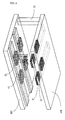
- FIG. 3 is a perspective view schematically illustrating a construction of an active-matrix field emission display having a gate plate according to the present invention
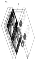
- FIG. 4 is a perspective view schematically illustrating a cathode plate, a gate plate and an anode plate in a field emission display according to the present invention.
- the field emission display includes the cathode plate 100, the gate plate 200 and the anode plate 300.
- the cathode plate 100 includes a belt shaped row signal line 120S and column signal line 120D on an insulating substrate 110 including glass, plastic, various ceramics, and the like, wherein the belt shaped row signal line and column signal line are made of a metal and enable to a row/column addressing.
- the unit pixels are defined by the row signal lines 120S and the column signal lines 120D.
- Each pixel includes a film-shaped (thin film or thick film) field emitter 130 made of diamond, diamond like carbon, carbon nanotube, etc. and a control device 140 of the field emitter. It is preferred that the control device 140 includes two terminals connected to at least the row signal line 120S and the column signal line 120D and one terminal connected to the film-shaped field emitter 130.
- the control device 140 may be an amorphous thin film transistor, a polysilicon thin film transistor, a metal-oxide-semiconductor field effect transistor, or the like.
- the gate plate 200 includes gate holes 220 penetrating a substrate 210, and a gate electrode 230 made of a metal around the gate holes 220.
- the substrate 210 of the gate plate 200 can be formed by a transparent substrate such as glass, plastic, various ceramics, various transparent insulating substrates, or the like, and if necessary, a non-transparent substrate can be used as the substrate.
- the thickness of the gate plate 200 may be for example 0.01 to 1.1 mm and the thickness of the gate electrode may be several hundreds of ⁇ to several thousands of ⁇ .
- the metal used for the gate electrode 230 may be chrome, aluminum, molybdenum, and the like, but not limited thereto.
- the gate holes 220 can be formed to be opened a little bit larger than each pixel so that the holes 220 can serve as the aperture of the unit pixel (for example, several tens of ⁇ m to several hundreds of ⁇ m) formed in the cathode plate 100.
- the size of the gate hole 220, the shape of the section, the thickness of the gate plate 200, the thickness of the gate electrode 230, the shape and distance separated from the field emitter 130, etc. are not specially limited but can be variously modified.
- the anode plate 300 includes a transparent electrode 320, and phosphors 330 of red (R), green (G) and blue (B) formed on a portion of the transparent electrode 320, on a transparent insulating substrate 310 made of glass, plastic, various ceramics, etc., as shown in FIG. 4.
- the cathode plate 100, the gate plate 200 and the anode plate 300, the field emitter 130 of the cathode plate 100 are vacuum packaged parallel to the phosphor 330 of the anode plate 300 through the gate holes 220 of the gate plate 200, while facing each other, by means of using spacers 400 as a supporter, as shown in FIG. 3 and FIG. 4.
- the spacers 400 can be manufactured by glass beads, ceramics, polymer, etc. and may have a height in the range of approximately 200 ⁇ m to 3mm.
- the gate electrode 230 may be also used as an optical-shielding film by selecting the type of a metal used as the gate electrode 230 or the thickness of the film.
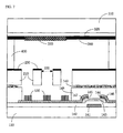
- FIG. 5 is a cross-sectional view illustrating the unit pixel of the field emission display according to the present invention.
- the gate plate is adhered to the cathode plate, while the anode plate is separated and vacuum packaged from the gate plate by the spacer supported between the anode plate and the gate plate.
- the cathode plate, the gate plate and the anode plate can be fabricated separately and then combined together.
- the unit pixel of the field emission display shown in FIG. 5 includes the cathode plate, the gate plate and the anode plate.
- the cathode plate has the substrate 110, the thin film transistor element, the field emitter, etc.
- the thin film transistor element includes a gate 141 made of a metal on the substrate 110, a gate insulating film of the thin film transistor 142 composed of an amorphous silicon nitride (a-SiNx) film or a silicon oxide film on the substrate 110 including the gate 141, an active layer of the thin film transistor 143 formed of amorphous silicon (a-Si) on a portion of the gate 141 and the gate insulating film 142, a source 144 and a drain 145 of the thin film transistor formed of n-type amorphous silicon at both ends of the active layer 143, a source electrode 146 of the thin film transistor formed of a metal on a portion of the source 144 and the gate insulating film 142, a drain electrode 147 of the thin film transistor formed of a metal on a portion of the drain 145 and the gate insulating film 142, a source electrode 146 of the thin film transistor, and an interlayer insulating film (passivation insulating film) 148 composed
- an electron-convergence electrode 149 formed of a metal may be intervened on a portion of the interlayer insulating film 148.
- the electron-convergence electrode 149 can serve as an optical-shielding film and perform the function of focusing the electrons emitted from the field emitter 130, by applying for a proper voltage.
- the field emitter 130 may be formed of diamond, diamond like carbon, carbon nanotube, and the like on a portion of the drain electrode 147 of the thin film transistor.
- the surface of the gate plate having no gate electrode 230 is adhered to the cathode plate.
- said gate plate are arranged in accordance with the field emitter 130 of the cathode plate, the anode plate are separated from the gate plate by using the spacers 400 as the supporter between them.
- said anode plate is arranged and vacuum packaged against the phosphor 330 of the anode plate and the field emitter 130 of the cathode plate.
- the spacers 400 serve to keep isolation between the cathode plate/the gate plate and the anode plate. It is not necessarily to be installed in every pixel.
- the gate plate includes the gate holes 220 formed by penetrating the glass substrate 210 and the gate electrode 230 made of a metal around the gate holes 220.
- the anode plate includes the transparent electrode 320 formed on a portion of the substrate 310, phosphors 330 of red, green and blue formed on a portion of the transparent electrode 320, and a black matrix 340 formed between said phosphors 330.
- the gate plate and the cathode plate can be fabricated separately, the manufacturing process can be readily performed and the gate insulating film in the field emitter fundamentally can be removed. Therefore, the separately fabricated gate plate, the cathode plate and the anode plate are combined together. As a result, it is possible to significantly improve the manufacturing productivity and yield of the field emission display.
- a DC voltage of 50 to 1500V is applied to the gate electrode 230 of the gate plate to induce an electron emission from a film-shaped field emitter 130 of the cathode plate.
- said emitted electrons are accelerated with high energy by applying a high voltage of above 2kV to the transparent electrode 320 of the anode plate.
- an operation of a control device of the field emitter in each pixel of the cathode plate can be controlled, by adjusting the voltages applied to the row signal line 120S and the column signal line 120D of the display.
- the control device 140 of the field emitter in each pixel represents an image by controlling an electron emission of the field emitter 130.
- the voltage applied to the gate electrode 230 of the gate plate serves to prohibit electron emission of the field emitter by the anode voltage, and also prevent local arching by forming a relatively uniform potential between the anode plate and the gate plate.
- the voltage applied to the row signal line 120S and the column signal line 120D of the display is applied to the gate and the source of the thin film transistor.
- the voltage applied to the gate of thin film transistor may be over 5V to below 50V when the thin film transistor having the active layer formed of amorphous silicon is turned on and below 5V or a negative voltage when the transistor is turned off. Further, the voltage applied to the source may be approximately in the range of 0 to 50 V.
- the control of the applied voltage, as described above, can be made by an external driver circuit (not shown).
- Gray scale representation of the common field emission display is implemented using a pulse width modulation (PWM) mode.
- PWM pulse width modulation
- This is the mode that the duration of the voltage of the data signal applied to the field emitter is controlled to represent gray scale.
- gray scale is represented by the difference in the amount of the electrons emitted for a given time. In other words, if there are plenty of the amounts in the electrons for a given time, a corresponding pixel emits a light having high brightness.
- the mode has a critical limitation where the width (time) of the pulse assigned to the unit pixel is gradually reduced in implementing a large-scale, high-resolution screen. Further, it has a problem that it is difficult to exactly control the amount of emitted electrons.
- Gray scale representation of the field emission display may use the pulse width modulation (PWM) mode or the pulse amplitude (PAM) mode separately, or a combination of them.
- PWM pulse width modulation
- PAM pulse amplitude
- the PAM mode is that gray scale is represented based on the difference of the amplitude applied as the data signal.
- This mode employs that the amount of the electrons transported to the field emitter may be varied by the difference in the level of the voltage applied to the source in a state where the thin film transistor is turned on.
- Gray scale can be represented by differentiating the level into two or more levels. This driving method can be applied to implement the large-scale screen and control electrons emission constantly.
- a constant voltage may be applied to the electron-convergence electrode 149 in order to help the electrons emitted from the field emitter 130 of the cathode plate to be well converged on the phosphor 330 of the anode plate, and also, to prohibit field emission of the field emitter 130 by the anode voltage along with the gate electrode 230 of the gate plate.
- the electron-convergence electrode 149 as the optical-shielding film, it is possible to prevent the active layer of the thin film transistor 143 from being exposed to the phosphor of the anode plate or surrounding lights.
- FIG. 6 is a cross-sectional view illustrating a pixel structure of a field emission display according to another embodiment of the present invention.
- FIG. 6 The structures of a cathode plate, a gate plate and an anode plate in FIG. 6 are the same as those of FIG. 5, except that the portion into which spacers 400 are inserted is between the gate plate and the cathode plate. In other words, the surface of the gate plate not having a gate electrode 230 is adhered to the anode plate.
- FIG. 7 is a cross-sectional view illustrating a pixel structure of a field emission display according to still another embodiment of the present invention.
- the structure of the anode plate in FIG. 7 is the same as that of FIG. 5, except that the field emitter 130 of the cathode plate has a plurality of dots and there are many the gate holes 220 of the gate plate so that they are coincident with the number of the dots of the field emitter 130 in the cathode plate.
- Such a structure has an effective advantage in applying a high voltage to the electrode of the anode plate. In addition, it can prevent the anode electric field from exerting a harmful influence on the field emitter through the plurality of the dots.
- FIG. 8 is a cross-sectional view illustrating a pixel structure of a field emission display according to further another embodiment of the present invention.
- gate holes 220 of the gate plate has a dual hole including a larger hole than the phosphor 340 of the anode plate and a small hole corresponding to the field emitter 130 of the cathode plate, the surface of the gate plate having no gate electrode 230 is adhered to the anode plate, and the cathode plate is formed by vacuum packaging in a state where the cathode plate and the gate plate are separated with the spacers supported between them.
- the field emission display includes a cathode plate, a gate plate, and an anode plate and the gate holes of the gate plate may have an inclined inner wall.
- the gate hole having the inclined inner wall serves to focus an electron, which is emitted from the field emitter, on a phosphor of the anode.
- the field emission display includes a cathode plate and an anode plate.
- An insulating layer may be formed on an each upper part of the cathode plates of Fig 5 to 8 in which a filed emitter, a control device, and so on are formed without having an additional gate plate.
- the insulating layer includes a gate hole having an inclined inner wall.
- a gate electrode is formed around the top of the gate hole.
- the insulating layer can be formed using various materials that are not specially confined.
- the insulating layer is formed with a thickness in the range of 0.01mm to 2mm.
- the inclined inner wall in the gate hole of the insulating layer can be formed in such a manner that a plurality of insulating layers each having a different etching ratio are formed and then etched by means of a wet etching method, or a green sheet that is made by stacking insulators each having a different etching ratio is attached to a cathode plate by means of a lamination method, and then annealed and etched.
- the field emitter according to the other variation is composed of one dot.
- the field emitter comprises a plurality of dots and the number of the gate holes corresponds to those of the dots in the field emitter of the cathode plate.
- a field emission display includes an anode plate consisting of a glass substrate, a cathode plate and a gate plate.
- the cathode plate includes signal lines for which row/column addressing is possible and pixels each defined by the row/column signal lines, wherein each pixel has a film-shaped field emitter and a control device of the field emitter.
- the row/column driving voltage of the display can be reduced significantly by inputting and driving scan and data signals of the display to the control device of each pixel. Therefore, a cheap low-voltage driving circuit can be used instead of a high-voltage driving circuit that is required for row/column driving of the conventional field emission display.
- the present invention since the electric field for field emission can be applied through the gate electrode of the gate plate, the distance between the anode plate and the cathode plate can be freely controlled, thereby a high voltage can be applied to the anode. Therefore, the present invention has an advantageous effect that it can significantly increase the brightness of the field emission display. Further, the voltage applied to the gate electrode of the gate plate serves to prohibit electron emission of the field emitter by the anode voltage, and also prevent local arching by forming a relatively uniform potential between the anode plate and the gate plate. Thus the life of the field emission display can be improved significantly.
- the gate plate and the cathode plate can be fabricated separately and then assembled together, manufacturing process can be readily performed and a breakdown of a gate insulating film in the field emitter can be removed fundamentally.
- the present invention can be provided to improve the manufacturing productivity and yield of the field emission display significantly.
- the gate hole having the inclined inner wall serves to focus an electron, which is emitted from the field emitter, on a phosphor of the anode.
- the field emission display having a high resolution can be produced without an additional focusing grid.
Landscapes
- Cathode-Ray Tubes And Fluorescent Screens For Display (AREA)
- Control Of Indicators Other Than Cathode Ray Tubes (AREA)
- Electrodes For Cathode-Ray Tubes (AREA)
- Vessels, Lead-In Wires, Accessory Apparatuses For Cathode-Ray Tubes (AREA)
Applications Claiming Priority (4)
| Application Number | Priority Date | Filing Date | Title |
|---|---|---|---|
| KR2002083754 | 2002-12-24 | ||
| KR20020083754 | 2002-12-24 | ||
| KR2003020781 | 2003-04-02 | ||
| KR10-2003-0020781A KR100517821B1 (ko) | 2002-12-24 | 2003-04-02 | 게이트 판을 구비하는 전계 방출 디스플레이 |
Publications (3)
| Publication Number | Publication Date |
|---|---|
| EP1437756A2 true EP1437756A2 (de) | 2004-07-14 |
| EP1437756A3 EP1437756A3 (de) | 2007-07-11 |
| EP1437756B1 EP1437756B1 (de) | 2009-10-28 |
Family
ID=32510717
Family Applications (1)
| Application Number | Title | Priority Date | Filing Date |
|---|---|---|---|
| EP03029789A Expired - Lifetime EP1437756B1 (de) | 2002-12-24 | 2003-12-23 | Feldemissionsanzeigevorrichtung mit Gate-Platte |
Country Status (4)
| Country | Link |
|---|---|
| US (1) | US7309954B2 (de) |
| EP (1) | EP1437756B1 (de) |
| JP (1) | JP3954002B2 (de) |
| CN (1) | CN1510713A (de) |
Cited By (2)
| Publication number | Priority date | Publication date | Assignee | Title |
|---|---|---|---|---|
| EP2017873A1 (de) * | 2007-07-10 | 2009-01-21 | Samsung SDI Co., Ltd. | Elektronenemissionsvorrichtung |
| US9812465B2 (en) | 2009-07-03 | 2017-11-07 | Semiconductor Energy Laboratory Co., Ltd. | Display device including transistor and manufacturing method thereof |
Families Citing this family (14)
| Publication number | Priority date | Publication date | Assignee | Title |
|---|---|---|---|---|
| TW511108B (en) * | 2001-08-13 | 2002-11-21 | Delta Optoelectronics Inc | Carbon nanotube field emission display technology |
| KR20060009681A (ko) * | 2004-07-26 | 2006-02-01 | 삼성에스디아이 주식회사 | 탄소나노튜브 에미터를 구비하는 전계 방출 디스플레이 및그 제조 방법 |
| KR20060011668A (ko) * | 2004-07-30 | 2006-02-03 | 삼성에스디아이 주식회사 | 전자 방출 소자와 이의 제조 방법 |
| KR20060012782A (ko) * | 2004-08-04 | 2006-02-09 | 삼성에스디아이 주식회사 | 전계방출소자와, 이를 적용한 전계방출 표시소자 |
| JP4417855B2 (ja) | 2005-01-05 | 2010-02-17 | 株式会社ノリタケカンパニーリミテド | 平面ディスプレイ、ゲート電極構造体およびゲート電極構造体の製造方法 |
| CN100339932C (zh) * | 2005-03-24 | 2007-09-26 | 中山大学 | 一种多层结构场发射显示器 |
| US20090295271A1 (en) * | 2005-04-01 | 2009-12-03 | Zhongshan University | Field Emission Display Having Multi-Layer Structure |
| KR100651624B1 (ko) * | 2005-11-10 | 2006-12-01 | 한국전자통신연구원 | 액티브-매트릭스 전계 방출 디스플레이 |
| TWI331374B (en) * | 2006-03-23 | 2010-10-01 | Unimicron Technology Corp | Carbon nanotube field emitting display |
| CN101636810B (zh) * | 2006-12-29 | 2011-11-23 | 塞莱斯系统集成公司 | 高频冷阴极三极型场发射真空管及其制造过程 |
| CN106019653B (zh) * | 2016-07-22 | 2019-04-23 | 京东方科技集团股份有限公司 | 假压头组件 |
| CN113200513B (zh) * | 2021-04-29 | 2023-11-24 | 中山大学南昌研究院 | 一种高度可控的电容加速度计封装的方法 |
| CN113517166A (zh) * | 2021-07-12 | 2021-10-19 | 葛伟 | 一种微阵列平板显示器件 |
| WO2023197123A1 (zh) * | 2022-04-12 | 2023-10-19 | 华为技术有限公司 | 电子源芯片及其制作方法、电子设备 |
Citations (2)
| Publication number | Priority date | Publication date | Assignee | Title |
|---|---|---|---|---|
| EP0708472A1 (de) | 1994-10-21 | 1996-04-24 | Yamaha Corporation | Herstellung eines Mikro-Elektronenemitters |
| US6380671B1 (en) | 1999-07-16 | 2002-04-30 | Samsung Sdi Co., Ltd. | Fed having a carbon nanotube film as emitters |
Family Cites Families (27)
| Publication number | Priority date | Publication date | Assignee | Title |
|---|---|---|---|---|
| US5015912A (en) | 1986-07-30 | 1991-05-14 | Sri International | Matrix-addressed flat panel display |
| JPH05182609A (ja) * | 1991-12-27 | 1993-07-23 | Sharp Corp | 画像表示装置 |
| JP2661457B2 (ja) | 1992-03-31 | 1997-10-08 | 双葉電子工業株式会社 | 電界放出形カソード |
| US5616991A (en) | 1992-04-07 | 1997-04-01 | Micron Technology, Inc. | Flat panel display in which low-voltage row and column address signals control a much higher pixel activation voltage |
| JPH07104679A (ja) | 1993-09-30 | 1995-04-21 | Futaba Corp | 電界放出形蛍光表示装置 |
| US5528103A (en) * | 1994-01-31 | 1996-06-18 | Silicon Video Corporation | Field emitter with focusing ridges situated to sides of gate |
| JPH07335117A (ja) | 1994-06-03 | 1995-12-22 | Nippon Steel Corp | 駆動回路一体型電子銃、駆動回路一体型電子銃アレイ、およびこれらの製造方法 |
| JP2809129B2 (ja) * | 1995-04-20 | 1998-10-08 | 日本電気株式会社 | 電界放射冷陰極とこれを用いた表示装置 |
| KR100233254B1 (ko) * | 1996-12-21 | 1999-12-01 | 정선종 | 전계 방출 디스플레이 |
| JPH10283958A (ja) | 1997-04-07 | 1998-10-23 | Canon Inc | 電子管及び画像表示装置 |
| KR100301242B1 (ko) | 1998-11-30 | 2001-09-06 | 오길록 | 전계방출디스플레이장치 |
| KR100319453B1 (ko) * | 1999-08-04 | 2002-01-05 | 오길록 | 2극형 전계 에미터를 가진 전계 방출 디스플레이 |
| US6756729B1 (en) | 1999-08-23 | 2004-06-29 | Samsung Sdi Co., Ltd. | Flat panel display and method of fabricating same |
| JP3863325B2 (ja) | 1999-09-10 | 2006-12-27 | 株式会社日立製作所 | 画像表示装置 |
| JP4132502B2 (ja) | 1999-11-24 | 2008-08-13 | 株式会社ノリタケカンパニーリミテド | 平面ディスプレイ及びその製造方法 |
| JP2001167720A (ja) | 1999-12-07 | 2001-06-22 | Natl Inst Of Advanced Industrial Science & Technology Meti | 平面ディスプレイ |
| JP2001222967A (ja) | 2000-02-07 | 2001-08-17 | Sony Corp | 電界放出型表示装置およびその製造方法 |
| JP4670137B2 (ja) * | 2000-03-10 | 2011-04-13 | ソニー株式会社 | 平面型表示装置 |
| JP2001266737A (ja) | 2000-03-24 | 2001-09-28 | Toshiba Corp | 電子源装置、その製造方法、および電子源装置を備えた平面表示装置 |
| KR100343205B1 (ko) | 2000-04-26 | 2002-07-10 | 김순택 | 카본나노튜브를 이용한 삼극 전계 방출 어레이 및 그 제작방법 |
| KR100363219B1 (ko) | 2000-09-01 | 2002-12-05 | 삼성에스디아이 주식회사 | 전계방출 표시장치 |
| KR100378597B1 (ko) * | 2000-12-22 | 2003-04-03 | 한국전자통신연구원 | 고해상도 전계 방출 디스플레이 |
| JP2002297083A (ja) | 2001-03-30 | 2002-10-09 | Matsushita Electric Ind Co Ltd | 画像表示装置 |
| JP4369075B2 (ja) | 2001-05-16 | 2009-11-18 | 株式会社ノリタケカンパニーリミテド | 平面ディスプレイ |
| JP2002367542A (ja) * | 2001-06-11 | 2002-12-20 | Mitsubishi Electric Corp | 電界放出型ディスプレイとその製造方法 |
| JP2003016913A (ja) | 2001-07-02 | 2003-01-17 | Canon Inc | 電子放出素子,電子源及び画像形成装置並びに電子放出素子の製造方法 |
| TWI283427B (en) * | 2001-07-12 | 2007-07-01 | Semiconductor Energy Lab | Display device using electron source elements and method of driving same |
-
2003
- 2003-10-02 JP JP2003344920A patent/JP3954002B2/ja not_active Expired - Fee Related
- 2003-12-23 US US10/745,736 patent/US7309954B2/en not_active Expired - Lifetime
- 2003-12-23 EP EP03029789A patent/EP1437756B1/de not_active Expired - Lifetime
- 2003-12-24 CN CNA200310114772XA patent/CN1510713A/zh active Pending
Patent Citations (2)
| Publication number | Priority date | Publication date | Assignee | Title |
|---|---|---|---|---|
| EP0708472A1 (de) | 1994-10-21 | 1996-04-24 | Yamaha Corporation | Herstellung eines Mikro-Elektronenemitters |
| US6380671B1 (en) | 1999-07-16 | 2002-04-30 | Samsung Sdi Co., Ltd. | Fed having a carbon nanotube film as emitters |
Cited By (9)
| Publication number | Priority date | Publication date | Assignee | Title |
|---|---|---|---|---|
| EP2017873A1 (de) * | 2007-07-10 | 2009-01-21 | Samsung SDI Co., Ltd. | Elektronenemissionsvorrichtung |
| US9812465B2 (en) | 2009-07-03 | 2017-11-07 | Semiconductor Energy Laboratory Co., Ltd. | Display device including transistor and manufacturing method thereof |
| US9837441B2 (en) | 2009-07-03 | 2017-12-05 | Semiconductor Energy Laboratory Co., Ltd. | Display device including transistor and manufacturing method thereof |
| US10211231B2 (en) | 2009-07-03 | 2019-02-19 | Semiconductor Energy Laboratory Co., Ltd. | Display device including transistor and manufacturing method thereof |
| US10714503B2 (en) | 2009-07-03 | 2020-07-14 | Semiconductor Energy Laboratory Co., Ltd. | Display device including transistor and manufacturing method thereof |
| US11257847B2 (en) | 2009-07-03 | 2022-02-22 | Semiconductor Energy Laboratory Co., Ltd. | Display device including transistor and manufacturing method thereof |
| US11637130B2 (en) | 2009-07-03 | 2023-04-25 | Semiconductor Energy Laboratory Co., Ltd. | Display device including transistor and manufacturing method thereof |
| US11978741B2 (en) | 2009-07-03 | 2024-05-07 | Semiconductor Energy Laboratory Co., Ltd. | Display device including transistor and manufacturing method thereof |
| US12272698B2 (en) | 2009-07-03 | 2025-04-08 | Semiconductor Energy Laboratory Co., Ltd. | Semiconductor device comprising driver circuit |
Also Published As
| Publication number | Publication date |
|---|---|
| US7309954B2 (en) | 2007-12-18 |
| EP1437756B1 (de) | 2009-10-28 |
| US20040160161A1 (en) | 2004-08-19 |
| JP3954002B2 (ja) | 2007-08-08 |
| JP2004207222A (ja) | 2004-07-22 |
| CN1510713A (zh) | 2004-07-07 |
| EP1437756A3 (de) | 2007-07-11 |
Similar Documents
| Publication | Publication Date | Title |
|---|---|---|
| EP1596415B1 (de) | Feldemissionsanzeige | |
| EP1437756B1 (de) | Feldemissionsanzeigevorrichtung mit Gate-Platte | |
| US6538391B1 (en) | Image display and a manufacturing method of the same | |
| JP4001460B2 (ja) | 大領域fed装置及び方法 | |
| JP4424622B2 (ja) | 発光装置及び表示装置 | |
| US20060220527A1 (en) | Electron emission device, electron emission display device using the same and method of manufacturing the same | |
| US7141923B2 (en) | Field emission display in which a field emission device is applied to a flat display | |
| US7116291B1 (en) | Image display and method of driving image display | |
| CN1146944C (zh) | 降低场发射显示器中的电荷积累 | |
| US6683408B2 (en) | Electron-emitting device, electron source and image-forming apparatus | |
| US7514857B2 (en) | Electron emission device and electron emission display device using the same | |
| KR100517821B1 (ko) | 게이트 판을 구비하는 전계 방출 디스플레이 | |
| US20020030646A1 (en) | Highly bright field emission display device | |
| US20060267476A1 (en) | Electron emission device | |
| US20090001870A1 (en) | Image Display Apparatus | |
| HK1063530A (en) | Field emission display having gate plate | |
| EP1821329A2 (de) | Elektronenemissionsvorrichtung und Anzeigevorichtung damit | |
| KR100651624B1 (ko) | 액티브-매트릭스 전계 방출 디스플레이 | |
| KR20070078900A (ko) | 전자 방출 디바이스와 이를 이용한 전자 방출 표시디바이스 | |
| KR20080025532A (ko) | 전자 방출 디바이스 및 이를 이용한 전자 방출 디스플레이 |
Legal Events
| Date | Code | Title | Description |
|---|---|---|---|
| PUAI | Public reference made under article 153(3) epc to a published international application that has entered the european phase |
Free format text: ORIGINAL CODE: 0009012 |
|
| AK | Designated contracting states |
Kind code of ref document: A2 Designated state(s): AT BE BG CH CY CZ DE DK EE ES FI FR GB GR HU IE IT LI LU MC NL PT RO SE SI SK TR |
|
| AX | Request for extension of the european patent |
Extension state: AL LT LV MK |
|
| PUAL | Search report despatched |
Free format text: ORIGINAL CODE: 0009013 |
|
| AK | Designated contracting states |
Kind code of ref document: A3 Designated state(s): AT BE BG CH CY CZ DE DK EE ES FI FR GB GR HU IE IT LI LU MC NL PT RO SE SI SK TR |
|
| AX | Request for extension of the european patent |
Extension state: AL LT LV MK |
|
| 17P | Request for examination filed |
Effective date: 20080110 |
|
| AKX | Designation fees paid |
Designated state(s): AT BE BG CH CY CZ DE DK EE ES FI FR GB GR HU IE IT LI LU MC NL PT RO SE SI SK TR |
|
| 17Q | First examination report despatched |
Effective date: 20080222 |
|
| GRAP | Despatch of communication of intention to grant a patent |
Free format text: ORIGINAL CODE: EPIDOSNIGR1 |
|
| GRAS | Grant fee paid |
Free format text: ORIGINAL CODE: EPIDOSNIGR3 |
|
| GRAA | (expected) grant |
Free format text: ORIGINAL CODE: 0009210 |
|
| AK | Designated contracting states |
Kind code of ref document: B1 Designated state(s): AT BE BG CH CY CZ DE DK EE ES FI FR GB GR HU IE IT LI LU MC NL PT RO SE SI SK TR |
|
| REG | Reference to a national code |
Ref country code: GB Ref legal event code: FG4D |
|
| REG | Reference to a national code |
Ref country code: CH Ref legal event code: EP |
|
| REG | Reference to a national code |
Ref country code: IE Ref legal event code: FG4D |
|
| REF | Corresponds to: |
Ref document number: 60329819 Country of ref document: DE Date of ref document: 20091210 Kind code of ref document: P |
|
| NLV1 | Nl: lapsed or annulled due to failure to fulfill the requirements of art. 29p and 29m of the patents act | ||
| PG25 | Lapsed in a contracting state [announced via postgrant information from national office to epo] |
Ref country code: PT Free format text: LAPSE BECAUSE OF FAILURE TO SUBMIT A TRANSLATION OF THE DESCRIPTION OR TO PAY THE FEE WITHIN THE PRESCRIBED TIME-LIMIT Effective date: 20100301 Ref country code: ES Free format text: LAPSE BECAUSE OF FAILURE TO SUBMIT A TRANSLATION OF THE DESCRIPTION OR TO PAY THE FEE WITHIN THE PRESCRIBED TIME-LIMIT Effective date: 20100208 Ref country code: SE Free format text: LAPSE BECAUSE OF FAILURE TO SUBMIT A TRANSLATION OF THE DESCRIPTION OR TO PAY THE FEE WITHIN THE PRESCRIBED TIME-LIMIT Effective date: 20091028 Ref country code: FI Free format text: LAPSE BECAUSE OF FAILURE TO SUBMIT A TRANSLATION OF THE DESCRIPTION OR TO PAY THE FEE WITHIN THE PRESCRIBED TIME-LIMIT Effective date: 20091028 |
|
| PG25 | Lapsed in a contracting state [announced via postgrant information from national office to epo] |
Ref country code: CY Free format text: LAPSE BECAUSE OF FAILURE TO SUBMIT A TRANSLATION OF THE DESCRIPTION OR TO PAY THE FEE WITHIN THE PRESCRIBED TIME-LIMIT Effective date: 20091028 Ref country code: SI Free format text: LAPSE BECAUSE OF FAILURE TO SUBMIT A TRANSLATION OF THE DESCRIPTION OR TO PAY THE FEE WITHIN THE PRESCRIBED TIME-LIMIT Effective date: 20091028 |
|
| PG25 | Lapsed in a contracting state [announced via postgrant information from national office to epo] |
Ref country code: AT Free format text: LAPSE BECAUSE OF FAILURE TO SUBMIT A TRANSLATION OF THE DESCRIPTION OR TO PAY THE FEE WITHIN THE PRESCRIBED TIME-LIMIT Effective date: 20091028 Ref country code: BE Free format text: LAPSE BECAUSE OF FAILURE TO SUBMIT A TRANSLATION OF THE DESCRIPTION OR TO PAY THE FEE WITHIN THE PRESCRIBED TIME-LIMIT Effective date: 20091028 |
|
| PG25 | Lapsed in a contracting state [announced via postgrant information from national office to epo] |
Ref country code: MC Free format text: LAPSE BECAUSE OF NON-PAYMENT OF DUE FEES Effective date: 20100701 Ref country code: DK Free format text: LAPSE BECAUSE OF FAILURE TO SUBMIT A TRANSLATION OF THE DESCRIPTION OR TO PAY THE FEE WITHIN THE PRESCRIBED TIME-LIMIT Effective date: 20091028 Ref country code: RO Free format text: LAPSE BECAUSE OF FAILURE TO SUBMIT A TRANSLATION OF THE DESCRIPTION OR TO PAY THE FEE WITHIN THE PRESCRIBED TIME-LIMIT Effective date: 20091028 Ref country code: EE Free format text: LAPSE BECAUSE OF FAILURE TO SUBMIT A TRANSLATION OF THE DESCRIPTION OR TO PAY THE FEE WITHIN THE PRESCRIBED TIME-LIMIT Effective date: 20091028 Ref country code: BG Free format text: LAPSE BECAUSE OF FAILURE TO SUBMIT A TRANSLATION OF THE DESCRIPTION OR TO PAY THE FEE WITHIN THE PRESCRIBED TIME-LIMIT Effective date: 20100128 |
|
| REG | Reference to a national code |
Ref country code: CH Ref legal event code: PL |
|
| PG25 | Lapsed in a contracting state [announced via postgrant information from national office to epo] |
Ref country code: CZ Free format text: LAPSE BECAUSE OF FAILURE TO SUBMIT A TRANSLATION OF THE DESCRIPTION OR TO PAY THE FEE WITHIN THE PRESCRIBED TIME-LIMIT Effective date: 20091028 Ref country code: SK Free format text: LAPSE BECAUSE OF FAILURE TO SUBMIT A TRANSLATION OF THE DESCRIPTION OR TO PAY THE FEE WITHIN THE PRESCRIBED TIME-LIMIT Effective date: 20091028 |
|
| PLBE | No opposition filed within time limit |
Free format text: ORIGINAL CODE: 0009261 |
|
| STAA | Information on the status of an ep patent application or granted ep patent |
Free format text: STATUS: NO OPPOSITION FILED WITHIN TIME LIMIT |
|
| GBPC | Gb: european patent ceased through non-payment of renewal fee |
Effective date: 20100128 |
|
| 26N | No opposition filed |
Effective date: 20100729 |
|
| PG25 | Lapsed in a contracting state [announced via postgrant information from national office to epo] |
Ref country code: LI Free format text: LAPSE BECAUSE OF NON-PAYMENT OF DUE FEES Effective date: 20091231 Ref country code: IE Free format text: LAPSE BECAUSE OF NON-PAYMENT OF DUE FEES Effective date: 20091223 Ref country code: GR Free format text: LAPSE BECAUSE OF FAILURE TO SUBMIT A TRANSLATION OF THE DESCRIPTION OR TO PAY THE FEE WITHIN THE PRESCRIBED TIME-LIMIT Effective date: 20100129 Ref country code: CH Free format text: LAPSE BECAUSE OF NON-PAYMENT OF DUE FEES Effective date: 20091231 |
|
| PG25 | Lapsed in a contracting state [announced via postgrant information from national office to epo] |
Ref country code: GB Free format text: LAPSE BECAUSE OF NON-PAYMENT OF DUE FEES Effective date: 20100128 |
|
| PG25 | Lapsed in a contracting state [announced via postgrant information from national office to epo] |
Ref country code: IT Free format text: LAPSE BECAUSE OF FAILURE TO SUBMIT A TRANSLATION OF THE DESCRIPTION OR TO PAY THE FEE WITHIN THE PRESCRIBED TIME-LIMIT Effective date: 20091028 |
|
| PG25 | Lapsed in a contracting state [announced via postgrant information from national office to epo] |
Ref country code: LU Free format text: LAPSE BECAUSE OF NON-PAYMENT OF DUE FEES Effective date: 20091223 |
|
| PG25 | Lapsed in a contracting state [announced via postgrant information from national office to epo] |
Ref country code: HU Free format text: LAPSE BECAUSE OF FAILURE TO SUBMIT A TRANSLATION OF THE DESCRIPTION OR TO PAY THE FEE WITHIN THE PRESCRIBED TIME-LIMIT Effective date: 20100429 |
|
| PG25 | Lapsed in a contracting state [announced via postgrant information from national office to epo] |
Ref country code: TR Free format text: LAPSE BECAUSE OF FAILURE TO SUBMIT A TRANSLATION OF THE DESCRIPTION OR TO PAY THE FEE WITHIN THE PRESCRIBED TIME-LIMIT Effective date: 20091028 |
|
| PG25 | Lapsed in a contracting state [announced via postgrant information from national office to epo] |
Ref country code: NL Free format text: LAPSE BECAUSE OF FAILURE TO SUBMIT A TRANSLATION OF THE DESCRIPTION OR TO PAY THE FEE WITHIN THE PRESCRIBED TIME-LIMIT Effective date: 20091028 |
|
| PGFP | Annual fee paid to national office [announced via postgrant information from national office to epo] |
Ref country code: DE Payment date: 20121121 Year of fee payment: 10 |
|
| PGFP | Annual fee paid to national office [announced via postgrant information from national office to epo] |
Ref country code: FR Payment date: 20130104 Year of fee payment: 10 |
|
| REG | Reference to a national code |
Ref country code: DE Ref legal event code: R119 Ref document number: 60329819 Country of ref document: DE |
|
| REG | Reference to a national code |
Ref country code: FR Ref legal event code: ST Effective date: 20140829 |
|
| REG | Reference to a national code |
Ref country code: DE Ref legal event code: R119 Ref document number: 60329819 Country of ref document: DE Effective date: 20140701 |
|
| PG25 | Lapsed in a contracting state [announced via postgrant information from national office to epo] |
Ref country code: DE Free format text: LAPSE BECAUSE OF NON-PAYMENT OF DUE FEES Effective date: 20140701 |
|
| PG25 | Lapsed in a contracting state [announced via postgrant information from national office to epo] |
Ref country code: FR Free format text: LAPSE BECAUSE OF NON-PAYMENT OF DUE FEES Effective date: 20131231 |