EP1428335B1 - Erzeugung eines phasenregelkreisausgangssignals mit verringerten spektralen störkomponenten - Google Patents
Erzeugung eines phasenregelkreisausgangssignals mit verringerten spektralen störkomponenten Download PDFInfo
- Publication number
- EP1428335B1 EP1428335B1 EP02797983A EP02797983A EP1428335B1 EP 1428335 B1 EP1428335 B1 EP 1428335B1 EP 02797983 A EP02797983 A EP 02797983A EP 02797983 A EP02797983 A EP 02797983A EP 1428335 B1 EP1428335 B1 EP 1428335B1
- Authority
- EP
- European Patent Office
- Prior art keywords
- signal
- delay
- phase
- locked loop
- phase detector
- Prior art date
- Legal status (The legal status is an assumption and is not a legal conclusion. Google has not performed a legal analysis and makes no representation as to the accuracy of the status listed.)
- Expired - Lifetime
Links
- 230000003595 spectral effect Effects 0.000 title description 10
- 230000002452 interceptive effect Effects 0.000 claims abstract description 28
- 238000005070 sampling Methods 0.000 claims abstract description 13
- 238000000034 method Methods 0.000 claims description 17
- 230000000593 degrading effect Effects 0.000 claims description 7
- 230000000737 periodic effect Effects 0.000 claims description 6
- 230000001934 delay Effects 0.000 claims description 4
- 230000000694 effects Effects 0.000 abstract description 2
- 229920000729 poly(L-lysine) polymer Polymers 0.000 description 42
- 238000010586 diagram Methods 0.000 description 21
- 238000001228 spectrum Methods 0.000 description 7
- 230000003111 delayed effect Effects 0.000 description 4
- 230000008569 process Effects 0.000 description 4
- 238000004891 communication Methods 0.000 description 3
- 238000013459 approach Methods 0.000 description 2
- 238000012886 linear function Methods 0.000 description 2
- 230000004044 response Effects 0.000 description 2
- 230000004888 barrier function Effects 0.000 description 1
- 230000008859 change Effects 0.000 description 1
- 239000013078 crystal Substances 0.000 description 1
- 230000002939 deleterious effect Effects 0.000 description 1
- 238000001514 detection method Methods 0.000 description 1
- 238000010295 mobile communication Methods 0.000 description 1
- 230000010363 phase shift Effects 0.000 description 1
- 230000003252 repetitive effect Effects 0.000 description 1
- 230000009466 transformation Effects 0.000 description 1
Images


Classifications
-
- H—ELECTRICITY
- H03—ELECTRONIC CIRCUITRY
- H03L—AUTOMATIC CONTROL, STARTING, SYNCHRONISATION OR STABILISATION OF GENERATORS OF ELECTRONIC OSCILLATIONS OR PULSES
- H03L7/00—Automatic control of frequency or phase; Synchronisation
- H03L7/06—Automatic control of frequency or phase; Synchronisation using a reference signal applied to a frequency- or phase-locked loop
- H03L7/08—Details of the phase-locked loop
- H03L7/081—Details of the phase-locked loop provided with an additional controlled phase shifter
-
- H—ELECTRICITY
- H03—ELECTRONIC CIRCUITRY
- H03L—AUTOMATIC CONTROL, STARTING, SYNCHRONISATION OR STABILISATION OF GENERATORS OF ELECTRONIC OSCILLATIONS OR PULSES
- H03L7/00—Automatic control of frequency or phase; Synchronisation
- H03L7/06—Automatic control of frequency or phase; Synchronisation using a reference signal applied to a frequency- or phase-locked loop
- H03L7/08—Details of the phase-locked loop
- H03L7/085—Details of the phase-locked loop concerning mainly the frequency- or phase-detection arrangement including the filtering or amplification of its output signal
- H03L7/089—Details of the phase-locked loop concerning mainly the frequency- or phase-detection arrangement including the filtering or amplification of its output signal the phase or frequency detector generating up-down pulses
- H03L7/0891—Details of the phase-locked loop concerning mainly the frequency- or phase-detection arrangement including the filtering or amplification of its output signal the phase or frequency detector generating up-down pulses the up-down pulses controlling source and sink current generators, e.g. a charge pump
-
- H—ELECTRICITY
- H03—ELECTRONIC CIRCUITRY
- H03L—AUTOMATIC CONTROL, STARTING, SYNCHRONISATION OR STABILISATION OF GENERATORS OF ELECTRONIC OSCILLATIONS OR PULSES
- H03L7/00—Automatic control of frequency or phase; Synchronisation
- H03L7/06—Automatic control of frequency or phase; Synchronisation using a reference signal applied to a frequency- or phase-locked loop
- H03L7/16—Indirect frequency synthesis, i.e. generating a desired one of a number of predetermined frequencies using a frequency- or phase-locked loop
- H03L7/18—Indirect frequency synthesis, i.e. generating a desired one of a number of predetermined frequencies using a frequency- or phase-locked loop using a frequency divider or counter in the loop
- H03L7/197—Indirect frequency synthesis, i.e. generating a desired one of a number of predetermined frequencies using a frequency- or phase-locked loop using a frequency divider or counter in the loop a time difference being used for locking the loop, the counter counting between numbers which are variable in time or the frequency divider dividing by a factor variable in time, e.g. for obtaining fractional frequency division
- H03L7/1974—Indirect frequency synthesis, i.e. generating a desired one of a number of predetermined frequencies using a frequency- or phase-locked loop using a frequency divider or counter in the loop a time difference being used for locking the loop, the counter counting between numbers which are variable in time or the frequency divider dividing by a factor variable in time, e.g. for obtaining fractional frequency division for fractional frequency division
- H03L7/1976—Indirect frequency synthesis, i.e. generating a desired one of a number of predetermined frequencies using a frequency- or phase-locked loop using a frequency divider or counter in the loop a time difference being used for locking the loop, the counter counting between numbers which are variable in time or the frequency divider dividing by a factor variable in time, e.g. for obtaining fractional frequency division for fractional frequency division using a phase accumulator for controlling the counter or frequency divider
-
- H—ELECTRICITY
- H04—ELECTRIC COMMUNICATION TECHNIQUE
- H04B—TRANSMISSION
- H04B15/00—Suppression or limitation of noise or interference
- H04B15/02—Reducing interference from electric apparatus by means located at or near the interfering apparatus
- H04B15/04—Reducing interference from electric apparatus by means located at or near the interfering apparatus the interference being caused by substantially sinusoidal oscillations, e.g. in a receiver or in a tape-recorder
Definitions
- the present invention relates to frequency synthesizers and direct modulation, more particularly to phase locked loops, and even more particularly to phase detectors for use in a phase locked loop and exposed to interfering signals placed close to frequencies which are multiples of the reference frequency of the phase locked loop ("PLL").
- PLL phase locked loop
- PLLs are well known and are useful for generating oscillating signals in many types of circuits, including but not limited to radio circuitry.
- PLLs may be employed to effect continuous phase modulation (CPM) of a carrier signal.
- CPM continuous phase modulation
- U.S. Patent Application 09/580,632 entitled “Linear Dead-Band-Free Digital Phase Detection,” the contents of which are hereby incorporated herein by reference in their entirety.
- FIG. 1 is a block diagram of a conventional integer-divide PLL 100.
- a phase detector 101 compares the phase of a signal supplied by a reference oscillator 103 with the phase of a feedback signal supplied by a frequency divider 105.
- the output of the phase detector which represents the phase difference between the two input signals, is filtered by a filter 107.
- the filtered output is then used to control the frequency of an output signal generated by a voltage controlled oscillator (VCO) 109.
- VCO voltage controlled oscillator
- the output signal from the VCO 109 in addition to being supplied as an output from the PLL, is also supplied as an input to the frequency divider 105, and is thus the source of the feedback signal.
- fractional-N PLLs have been devised.
- a transmitter structure called a "Direct Modulation architecture" transmitter and Local Oscillator synthesizer
- a Direct Modulation architecture transmitter and Local Oscillator synthesizer
- the output RF signal of the PLL in a highly Integrated Direct Modulation architecture has a tendency to leak back to the reference parts of the PLL, such as the phase detector.
- the reference parts of the PLL such as the phase detector.
- this leaking RF signal is mixed with the original wanted baseband signal in the phase detector, a problem arises in that the signal generated at the output of the PLL includes spurious components at N times the reference frequency, where N equals an integer.
- any PLL exposed to an unwanted RF interferer placed at frequencies close to multiples of the reference frequency will experience problems with spurious spectral components at N times the reference frequency.
- US-A-6160456 and US-B-6219397 disclose examples of the prior art in this field. It is therefore desirable to provide a PLL that will reduce the problem of having N times the reference frequency spurious spectral components around the RF spectrum when using a Sigma-Delta controlled fractional-N PLL as a modulator or frequency synthesiser.
- a phase locked loop for reducing the amount of unwanted signals that interfere with the operation of the phase locked loop circuit
- the phase locked loop circuit comprising: a voltage controlled oscillator (VCO); a phase detector coupled between a frequency divider and the voltage controlled oscillator, the phase detector being connected to receive a moderated reference frequency, and operable to generate first and second signals, and a difference signal from the first and second signals; characterised by a controller operable to generate a modulating signal and to apply the modulating signal to the phase detector, thereby degrading the sampling performance of the phase detector such that the first and second signals and the difference signal are modulated in the time domain; and the single frequency divider being operable to receive a signal from the voltage controlled oscillator and a signal from the controller.
- VCO voltage controlled oscillator
- a method of generating an oscillating signal comprising: receiving a reference frequency signal; detecting a phase or frequency difference between the reference frequency signal and a feedback signal and generating first and second signals, and a difference signal from the first and second signals, representative of the phase or frequency difference, characterised by: generating an oscillating signal as a function of the difference signal; generating the feedback signal as a function of the oscillating signal; introducing a modulating signal to at least one of the reference frequency signal and the feedback signal prior to performing the step of detecting, thereby degrading the sampling performance of the detecting step, such that the first and second signals and the difference signals are modulated in the time domain; and operating on the oscillating signal by performing a frequency translation.
- a phase lock loop and method comprising a voltage controlled oscillator, a phase detector, and logic that degrades the sampling performance of the phase detector.
- the logic for degrading the sampling performance can be performed in a plurality of ways. One way is by introducing a controllable time delay that supplies a delayed signal to one of the phase detector signal inputs.
- the logic for degrading can also comprise applying an interfering analog signal to an input of the phase detector, wherein the input is associated with a stable internal phase detector signal. An additional interfering signal having a different frequency from that of the reference frequency of the PLL is applied to the phase detector input that produces a stable internal signal edge.
- the logic that degrades can also comprise at least two signal inputs of the phase detector and where a controllable delay is placed at both of the two signal inputs.
- the logic that degrades also comprises at least two signal inputs of the phase detector and where a controllable delay is placed at one of the two signal inputs
- the controllable delay is used to jitter at least one of the internal signal edges within the phase detector.
- One way of controlling the delay is to selectively apply one of two delays to an input signal based on a control signal.
- the controllable delay can be a NO delay and a predefined non-zero delay. Additionally, the controllable delay is selected from a plurality of different delay times.
- the controllable delay can also be controlled by a digital pseudo random bitstream which is binary for a two level delay setting.
- Another controllable delay is controlled by an M-ary digital pseudo random bitstream.
- the controllable delay can also be controlled by a periodic analog signal.
- the phase detector comprises at least one component of a Sigma Delta controlled fractional-N phase locked loop.
- a phase detector can act as a less than perfect sampler by introducing a time jitter on signal edges that enter the phase detector input.
- the present invention helps to mitigate and reduce the amount of interfering signals (e.g. RF leakage) that enter the phase detector. No additional non-linearities are introduced since all edges of the signals present in the phase detector are intended to be simultaneously time varying.
- a phase detector can be made to act as a less than perfect sampler by intentionally introducing an interfering signal.
- an interfering signal For example, a small interfering analog signal can be introduced with a different frequency from the reference frequency already present in the PLL.
- the interfering signal is applied at an input of the phase detector input that is associated with a stable internal phase detector signal.
- the interfering signal will cause the stable internal signal to vary slightly in time at the rate of the interfering signal frequency. It is this signal variation and jitter introduced on the signal edges entering the phase detector input that induces the phase detector to act as a less than perfect sampler.
- FIG. 2 is a block diagram of a digital dead band free phase/frequency detector 200 that may be used in a PLL.
- the use of first and second digital latches 212, 214 enables multiple states (not shown in FIG. 2) and, hence, an extended operating range of the phase detector 200.
- the first latch 212 controls whether a first charge pump 202 is on or off.
- the second latch 214 controls whether the second charge pump 205 is on or off.
- the first and second charge pumps 202, 205 are connected in series, with the phase detector output current, i e being related to whether none, one, or both of the first and second charge pumps 202, 205 are turned on.
- the amount of time that i e is non-zero is a function of the phase difference between the two input signals, 201 and 203. This is because the first of these signals to present a clocking edge causes the output of the corresponding latch to be asserted, which in turn, causes a corresponding one of the first and second charge pumps 202, 205 to turn on. When the clocking of the remaining input signal is subsequently asserted, it also causes the output of its corresponding latch to be asserted. This causes the other one of the first and second charge pumps 202, 205 to turn on.
- This state is only temporary, however, because the outputs of both the first and second latches 212, 214 are further supplied to respective inputs of a logical AND gate 208, whose output is supplied to a delay element 210. The delayed signal is then supplied to the RESET inputs of both the first and second latches 212, 214.
- the output of the AND gate 208 will be asserted as well, thereby resetting both latches 212 and 214 after the delay associated with the delay element 210.
- the first and second latches 212, 214 are now initialized to repeat the process again for the next cycle. It will be recognized that the output current i e is either a positive value (being supplied by the first charge pump 202) if the first input signal 201 leads the second input signal 203, or else it is a negative value (being drawn by the second charge pump 205) if the second input signal 203 leads the first input signal 201.
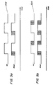
- FIGS. 3a and 3b illustrate two timing diagrams representing two different signal relationship scenarios that can occur within the phase detector of FIG. 2 when the PLL is in a locked steady state mode with modulation applied by the Sigma Delta modulator.
- the grey zones indicate time varying edges caused by the applied modulation. Modulation is applied by switching the division factor of the PLL.
- Timing diagram 300 of FIG. 3a illustrates the relative positions of the internal phase detector signals when the frequency divider signal is ahead of the reference signal. In this case, note that only one edge 302 of the "up” and “down” signals is varying in time. The remaining edges of these "up” and “down” signals are stable.
- the grey zones in both timing diagrams (e.g., zones 302, 304, 306 and 308) indicate respective time varying edges caused by the applied modulation.
- One exemplary method for achieving the applied modulation is by switching the division factor of the PLL.
- timing diagram 3.10 of FIG. 3b the alternative situation of having the reference signal ahead of the frequency division signal is shown. Under these conditions, three edges 312 of the "up” and “down” signals are varying in time. There still remains one stable edge 314, however, associated with the "up” signal.
- phase/frequency detector is dead band free: This means that the phase detector will be responsive to all phase differences between the reference signal and the frequency divider signal.
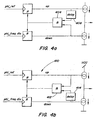
- FIGS. 4a and 4b respectively illustrate alternative embodiments 402, 410 of a digital linear dead band free phase/frequency detector.
- the delay element 406 is connected to the "up” signal and supplies a delayed "up” signal to the AND gate.
- the delay element 414 is connected to the "down” signal and supplies a delayed "down” signal to the AND gate.
- FIGS. 4a and 4b illustrate placing a delay element at either input path of the AND-gate. This results in a phase/frequency detector that is dead-band free and also works in a linear operating mode, since only one of the charge pump pulse lengths varies when modulation is applied.
- FIGS. 5a and 5b The timing diagrams for these types of phase detectors are shown in FIGS. 5a and 5b. It can be seen that these two types of prior art phase detectors generate "up” and “down” signals that have one or more stable signal edges, causing the unwanted sampling of the leaking RF signal. More specifically, the timing diagram 502 of FIG. 5a corresponds to phase/frequency detector configuration shown in FIG. 4a and timing diagram 504 corresponds to phase/frequency detector configuration 410 shown in FIG. 4b. In timing diagram 502, the "down” signal for the phase/frequency detector configuration 402 is depicted with grey zones representing the respective varying signal edges. The "up” signal for this configuration, however, has both leading and trailing edges that are stable. As shown in configuration timing diagram 504, the "up” signal generated by the phase/frequency detector configuration 410 has a leading edge that is stable. This results in an unwanted sampling of the leaking RF signal.
- FIG. 6a illustrates the different signals present in the PLL and explains the wanted and unwanted signals present in the PLL.
- the original RF signal 602 is operated on by the average division factor in the frequency divider 604. This operation places the RF signal at the desired location within the base band.
- the modulation bandwidth (that can be represented by a modulation index) of the original RF signal at baseband is the same as the modulation bandwidth at RF.
- the frequency divider 604 only operates on the RF signal by performing a frequency translation. This means that no transformation of modulation index is performed at this point in the process.
- the leaking RF path 606, as mentioned earlier, is coupled into the loop at the reference blocks 601 (crystal oscillator), 603 (squares the reference waveform) according to FIG. 6a.
- the unwanted RF signal at the reference input is mixed (folded/sampled) by the phase detector 605.
- the output of the phase detector 605 is forwarded to a filter 607 and then forwarded to the voltage controlled oscillator 609. Therefore, the unwanted signal will appear at a position in the base band with an offset equal to that found at RF between the reference multiple and the RF signal as shown in the graph of FIG. 6b.
- the total RF spectrum will be the product of the two base band spectrums shown in FIG. 6b. At the PLL output, this results in the wanted spectrum plus spurious spectral components at minus the delta offset 612 and a modulated sideband at plus the delta offset 610, if a modulated spectrum is generated in the Sigma-Delta controlled fractional-N PLL.
- phase detector act as an imperfect sampler to unwanted interfering signals.
- One way of doing this is to introduce a time jitter on the remaining stable edges of the "up” and “down” signals. No additional non-linearities are introduced by this technique since all edges of the signals working in the phase detector are intended to be simultaneously time varying.
- FIG. 7 illustrates one exemplary embodiment of the present invention.
- Controllable delay blocks 704, 702 are interposed between the reference signal and the frequency divider signal, respectively.
- the controllable delay blocks 704, 702 introduce a delay whose amount is controllable.
- the amount of variability of delay may differ from one embodiment to another.
- one or both of the controllable delay blocks 704, 702 may introduce either no delay or a fixed delay under the control of a binary signal.
- it is preferable although not essential to choose the delay amount such that it is substantially half of the radio frequency (RF) period; that is, to introduce a 180 degree phase shift.
- RF radio frequency
- the term "radio frequency” refers to the output frequency of the phase locked loop. This is because the optimum way of degrading the sampling process applied to the interfering signal in the phase detector is to, on average, sample the same amount of in-phase samples as out of phase samples of the interfering signal.
- one or both of the controllable delay blocks 704, 702 may have the capability of introducing any of a larger number of delay possibilities.
- a 2-bit control signal would be capable of selecting any of four possible delay values.
- controllable delay blocks 704, 702 are suitably controlled, a time jitter is introduced at the inputs of the phase/frequency detector. This time jitter will propagate through the PLL and also be applied to the signal edges controlling the charge pump.
- a delay control signal 701 is forwarded to one, both or none of the controllable delay elements 702 or 704. Different types of control signals may be used.
- the control signal may be a random sequence or a periodic sequence.
- the signal controlling the two input delay blocks shown in.FIG. 7 may be taken from one of the Sigma-Delta output signals providing the modulation (i.e., one of the signals that switch the division factor).
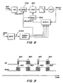
- FIG. 8 shows the controllable delay blocks 702, 704 incorporated into a Sigma-Delta controlled fractional-N PLL.
- the signal controlling the two controllable delay blocks 702, 704 is taken from one of the Sigma-Delta output signals providing the modulation (i.e., switching the division factor).
- FIG. 9 is a timing diagram that shows the introduced extra time jitter 901 caused by the controllable delay elements at the two inputs of the phase detector, assuming that the phase detector 801 is constructed as illustrated in FIG. 4b. Note that all flanks of the "up” and “down” signals are now varying in time. Without this extra jitter, the leading edges of the "up” signal would be stable, as previously illustrated in FIG. 5b. Similar results would be achieved in any of the other previously described phase detector embodiments.
- FIG. 10 illustrates another exemplary embodiment of the present invention.
- This embodiment reduces the sampling performance of the phase detector by using an interfering signal. More specifically, a small interfering analog signal is introduced that has a frequency differing from the reference frequency of the loop.
- the interfering signal is applied to those phase detector inputs that are responsible for producing a stable internal phase detector signal. For example, if the phase detector 1001 is constructed like the phase detector 410 shown in FIG. 4b, then the only stable edge is the leading edge of the "up" signal (see FIG. 5b). Consequently, the interfering signal may be applied to the reference input of the phase detector 1001.
- phase detector 1001. This may be done by using a combining circuit 1003 to combine the interfering signal with the reference signal and supplying the combined signal to the reference input of the phase detector 1001. If a different phase detector configuration is used, such as the phase detector 402 illustrated in FIG. 4a, then stable edges may also be associated with the "down" signal. (See, e.g., FIG. 5a.) In this case, the interfering signal should be applied to the frequency divider signal input of the phase detector 1001.
- the interfering signal will cause the stable internal signal to vary slightly in time at the rate of the interfering signal frequency.
- the frequency of this interfering signal should be different from the reference frequency. Assuming that the interfering signal is applied to only one of the inputs of the phase detector - 1001; a small noise contribution to the overall reference loop noise will be present in the loop, since this solution does not introduce a simultaneous time variation at both inputs of the phase detector 1001.
- the invention reduces the problem of having N times the reference frequency spurious spectral components around the RF spectrum when using a sigma delta controlled fractional-N PLL as a modulator or frequency synthesizer.
- a sigma delta controlled fractional-N PLL as a modulator or frequency synthesizer.
- the illustrated embodiments described above employ charge pumps, and generate an output current that varies as a substantially linear function of the phase difference between two signals.
- alternative embodiments of the invention can also be devised to generate an output voltage rather than an output current, wherein the output voltage varies as a substantially linear function of the phase difference between the two signals.
- voltage generators rather than charge pumps can be employed.
- the output voltage can serve as the source signal for controlling a VCO in a phase-locked loop, or the output voltage can alternatively be converted to a varying current for those embodiments that utilize a current controlled oscillator instead of a VCO.
- a controllable delay can be placed at the two signal inputs of a digital frequency/phase detector. This particular embodiment can jitter all internal signal flanks within the frequency/phase detector.
- the controllable delay may be implemented in binary form as "delay on/off', or as a controllable delay containing a complete set of different delays. Another way of controlling the delay may be by using a digital pseudo random bitstream which is binary for a two level delay setting or alternatively M-ary for a multilevel delay setting.
- the controllable delay may be controlled by a periodic analog signal, or by a periodic digital (binary or M-ary) sequence, depending on the number of delay levels implemented.
- any of the foregoing embodiments can be used in combination with the use of only one controllable delay at either one of the phase detector inputs.
- a third analog "interferer" signal having a different frequency from that of the reference frequency of the loop can be applied to the phase detector input responsible for producing a stable internal signal flank.
- any combination of the aforementioned embodiments can be used as a phase detector implementation in a Sigma Delta controlled fractional-N PLL or used as a phase detector implementation in any PLL which is exposed to an interfering RF signal placed close to frequencies that are multiples of the reference frequency of the PLL.
Landscapes
- Engineering & Computer Science (AREA)
- Computer Networks & Wireless Communication (AREA)
- Signal Processing (AREA)
- Stabilization Of Oscillater, Synchronisation, Frequency Synthesizers (AREA)
- Surface Acoustic Wave Elements And Circuit Networks Thereof (AREA)
- Gyroscopes (AREA)
Claims (19)
- Phasenregelkreis zum Reduzieren des Umfangs unerwarteter Signale, die den Betrieb des Phasenregelkreises stören, wobei der Phasenregelkreis umfasst:einen spannungsgesteuerten Oszillator (VCO);einen zwischen einer Frequenzteiler und dem spannungsgesteuerten Oszillator gekoppelten Phasendetektor (801, 1001), wobei der Phasendetektor erste und zweite Eingänge hat, die verbunden sind, um jeweils ein geteiltes Frequenzsignal von dem Frequenzteiler bzw. eine geminderte Referenzfrequenz zu empfangen, und betreibbar zum Erzeugen erster und zweiter Signale und eines Differenzsignals von den ersten und zweiten Signalen;eine Steuerung, die betreibbar ist zum Erzeugen eines modulierenden Signals und zum Anlegen des modulierenden Signals an den Phasendetektor, hierdurch die Abtastleistungsfähigkeit des Phasendetektors derart vermindernd, dass die ersten und zweiten Signale und das Differenzsignal im Zeitbereich moduliert werden; undwobei der einzelne Frequenzteiler betreibbar ist zum Empfangen eines Signals von dem spannungsgesteuerten Oszillator und eines Signals von der Steuerung,
wobei der Phasendetektor mindestens zwei Signalseingänge einschließt, und wobei die Steuerung dadurch gekennzeichnet ist, dass sie umfasst:eine Steuerungsverzögerungsschaltung, die betreibbar ist zum Zuführen einer identischen Verzögerung an die Signale der ersten und zweiten Eingänge des Phasendetektors. - Phasenregelkreis nach Anspruch 1, wobei die Steuerung eine Logik einschließt, die betreibbar ist zum Erzeugen eines Steuersignals, das die steuerbare Verzögerungsschaltung veranlasst, mindestens an einem der internen Signalflanken innerhalb des Phasendetektors ein Jitter-Verhalten zu zeigen.
- Phasenregelkreis nach Anspruch 1, wobei die steuerbare Verzögerungsschaltung betreibbar ist zum selektiven Anwenden einer von zwei Verzögerungen auf die ersten und zweiten Eingänge des Phasendetektors basierend auf einem Steuersignal.
- Phasenregelkreis nach Anspruch 3, wobei die beiden Verzögerungen keine Verzögerung und eine vordefinierte, von Null verschiedene Verzögerung sind.
- Phasenregelkreis nach Anspruch 4, wobei die vordefinierte, von Null verschiedene Verzögerung gleich der Hälfte einer Periodendauer eines Störsignals ist, das an einen der Phasendetektorsignaleingänge angelegt wird.
- Phasenregelkreis nach Anspruch 1, wobei die steuerbare Verzögerungsschaltung eine Verzögerungslogik umfasst, die betreibbar ist zum selektiven Anwenden einer von einer Vielzahl unterschiedlicher Verzögerungszeiten auf die ersten und zweiten Eingänge des Phasendetektors.
- Phasenregelkreis nach Anspruch 1, wobei die steuerbare Verzögerungsschaltung durch einen digitalen Pseudozufalls-Bit-Strom gesteuert wird.
- Phasenregelkreis nach Anspruch 7, wobei jedes Bit des digitalen Pseudozufalls-Bit-Stroms eine von zwei oder mehr Verzögerungseinstellungen auswählt.
- Phasenregelkreis nach Anspruch 1, wobei die steuerbare Verzögerungsschaltung durch einen M-wertigen digitalen Pseudozufalls-Bit-Strom gesteuert wird.
- Phasenregelkreis nach Anspruch 1, wobei die steuerbare Verzögerungsschaltung durch ein periodisches Analogsignal gesteuert wird.
- Sigma-Delta-gesteuerter Bruch-N-Phasenregelkreis, der den Phasenregelkreis von Anspruch 1 umfasst.
- Verfahren zum Erzeugen eines Oszillationssignals, die folgenden Schritte umfassend:Empfangen eines Referenzfrequenzsignals;Erfassen einer Phasen- oder Frequenzdifferenz zwischen dem Referenzfrequenzsignal und einem Rückkopplungssignal und Erzeugen ersten und zweiter Signale, und ein Differenzsignal von den ersten und zweiten Signalen, die repräsentativ sind in Bezug auf die Phasen- oder Frequenzdifferenz, gekennzeichnet durch:Erzeugen eines Oszillationssignals als eine Funktion des Differenzsignals;Erzeugen des Rückkopplungssignals als eine Funktion des Oszillationssignals;Einfügen eines modulierenden Signals in mindestens eines von dem Referenzfrequenzsignal und dem Rückkopplungssignal vor dem Durchführen des Schrittes des Erfassens, hierdurch die Abtastperformance des Erfassungsschrittes derart herabsetzend, dass die ersten und zweiten Signale und das Differenzsignal im Zeitbereich moduliert werden; undBetreiben auf dem Oszillationssignal durch Durchführen einer Frequenzumsetzung, dadurch gekennzeichnet, dassder Schritt des Einfügens eines modulierenden Signals das Einfügen einer identischen, zeitvarianten Verzögerung für beide Eingänge eines Phasendetektors umfasst.
- Verfahren nach Anspruch 12, ferner das Verwenden eines digitalen Pseudozufalls-Bit-Stroms zum Bestimmen der zeitvarianten Verzögerung umfassend.
- Verfahren nach Anspruch 13, wobei der digitale Pseudozufalls-Bit-Strom zwei oder mehr Verzögerungseinstellungen steuert.
- Verfahren nach Anspruch 13, wobei der digitale Pseudozufalls-Bit-Strom ein M-wertiger Digitalpseudozufalls-Bit-Strom ist. '
- Verfahren nach Anspruch 12, wobei die zeitvariante Verzögerung zwischen zwei Verzögerungswerten variiert.
- Verfahren nach Anspruch 16, wobei die beiden Verzögerungswerte keine Verzögerung und eine vordefinierte, von Null verschiedene Verzögerung sind.
- Verfahren nach Anspruch 17, wobei die vordefinierte, von Null verschiedene Verzögerung gleich der Hälfte einer Periode des Oszillationssignals ist.
- Verfahren nach Anspruch 17, ferner das Verwenden eines periodischen Analogsignals zum Bestimmen der zeitvarianten Verzögerung umfassend.
Priority Applications (1)
| Application Number | Priority Date | Filing Date | Title |
|---|---|---|---|
| EP06019202A EP1729432B1 (de) | 2001-09-12 | 2002-09-11 | Erzeugung von einem phasenverriegelten Schleifesignal mit reduzierten Störemissionen |
Applications Claiming Priority (3)
| Application Number | Priority Date | Filing Date | Title |
|---|---|---|---|
| US949845 | 1978-10-10 | ||
| US09/949,845 US6952138B2 (en) | 2001-09-12 | 2001-09-12 | Generation of a phase locked loop output signal having reduced spurious spectral components |
| PCT/EP2002/010201 WO2003024005A1 (en) | 2001-09-12 | 2002-09-11 | Generation of a phase locked loop output signal having reduced spurious spectral components |
Related Child Applications (1)
| Application Number | Title | Priority Date | Filing Date |
|---|---|---|---|
| EP06019202A Division EP1729432B1 (de) | 2001-09-12 | 2002-09-11 | Erzeugung von einem phasenverriegelten Schleifesignal mit reduzierten Störemissionen |
Publications (2)
| Publication Number | Publication Date |
|---|---|
| EP1428335A1 EP1428335A1 (de) | 2004-06-16 |
| EP1428335B1 true EP1428335B1 (de) | 2007-02-28 |
Family
ID=25489591
Family Applications (2)
| Application Number | Title | Priority Date | Filing Date |
|---|---|---|---|
| EP06019202A Expired - Lifetime EP1729432B1 (de) | 2001-09-12 | 2002-09-11 | Erzeugung von einem phasenverriegelten Schleifesignal mit reduzierten Störemissionen |
| EP02797983A Expired - Lifetime EP1428335B1 (de) | 2001-09-12 | 2002-09-11 | Erzeugung eines phasenregelkreisausgangssignals mit verringerten spektralen störkomponenten |
Family Applications Before (1)
| Application Number | Title | Priority Date | Filing Date |
|---|---|---|---|
| EP06019202A Expired - Lifetime EP1729432B1 (de) | 2001-09-12 | 2002-09-11 | Erzeugung von einem phasenverriegelten Schleifesignal mit reduzierten Störemissionen |
Country Status (5)
| Country | Link |
|---|---|
| US (1) | US6952138B2 (de) |
| EP (2) | EP1729432B1 (de) |
| AT (2) | ATE416522T1 (de) |
| DE (2) | DE60230202D1 (de) |
| WO (1) | WO2003024005A1 (de) |
Cited By (3)
| Publication number | Priority date | Publication date | Assignee | Title |
|---|---|---|---|---|
| CN103026629A (zh) * | 2010-07-28 | 2013-04-03 | 马维尔国际贸易有限公司 | 使用受控时钟抖动的分数杂散减小 |
| US9397647B2 (en) | 2010-07-28 | 2016-07-19 | Marvell World Trade Ltd. | Clock spurs reduction technique |
| CN103026629B (zh) * | 2010-07-28 | 2018-02-09 | 马维尔国际贸易有限公司 | 使用受控时钟抖动的分数杂散减小 |
Families Citing this family (14)
| Publication number | Priority date | Publication date | Assignee | Title |
|---|---|---|---|---|
| US7049852B2 (en) * | 2004-02-02 | 2006-05-23 | Melanson John L | Fractional-integer phase-locked loop system with a fractional-frequency-interval phase frequency detector |
| US7613249B1 (en) | 2004-04-21 | 2009-11-03 | Marvell International Ltd. | Spurious component reduction |
| DE102005050621B4 (de) * | 2005-10-21 | 2011-06-01 | Infineon Technologies Ag | Phasenregelkreis und Verfahren zum Betrieb eines Phasenregelkreises |
| US7482885B2 (en) * | 2005-12-29 | 2009-01-27 | Orca Systems, Inc. | Method of frequency synthesis for fast switching |
| US7519349B2 (en) * | 2006-02-17 | 2009-04-14 | Orca Systems, Inc. | Transceiver development in VHF/UHF/GSM/GPS/bluetooth/cordless telephones |
| JP2007295363A (ja) | 2006-04-26 | 2007-11-08 | Nec Electronics Corp | Pll回路、pll回路の干渉防止方法及びこのpll回路を搭載した光ディスク装置 |
| US20070252620A1 (en) * | 2006-04-28 | 2007-11-01 | Motorola, Inc. | Phase offset control phase-frequency detector |
| US7929929B2 (en) * | 2007-09-25 | 2011-04-19 | Motorola Solutions, Inc. | Method and apparatus for spur reduction in a frequency synthesizer |
| US8138840B2 (en) * | 2009-01-23 | 2012-03-20 | International Business Machines Corporation | Optimal dithering of a digitally controlled oscillator with clock dithering for gain and bandwidth control |
| US8866556B2 (en) * | 2009-02-27 | 2014-10-21 | Analog Bits, Inc. | Phase shift phase locked loop |
| TW201121246A (en) * | 2009-12-14 | 2011-06-16 | Univ Nat Taiwan | Frequency synthesizers |
| JP6809484B2 (ja) * | 2016-01-08 | 2021-01-06 | ソニー株式会社 | 同期回路および同期回路の制御方法 |
| WO2018224144A1 (en) | 2017-06-07 | 2018-12-13 | Telefonaktiebolaget Lm Ericsson (Publ) | Phase control of phase locked loop |
| CN113071508B (zh) * | 2021-06-07 | 2021-08-20 | 北京理工大学 | 一种dcps架构下的车辆协同能量管理方法和系统 |
Family Cites Families (11)
| Publication number | Priority date | Publication date | Assignee | Title |
|---|---|---|---|---|
| JPS63252014A (ja) * | 1987-04-08 | 1988-10-19 | Kokusai Denshin Denwa Co Ltd <Kdd> | 位相同期方式 |
| US5631920A (en) | 1993-11-29 | 1997-05-20 | Lexmark International, Inc. | Spread spectrum clock generator |
| CA2123477A1 (en) | 1994-05-12 | 1995-11-13 | Thomas Atkin Denning Riley | Delta-sigma fractional-n frequency synthesizer and frequency discriminator suitable for use therein |
| US5986512A (en) | 1997-12-12 | 1999-11-16 | Telefonaktiebolaget L M Ericsson (Publ) | Σ-Δ modulator-controlled phase-locked-loop circuit |
| EP0940922B1 (de) | 1998-03-03 | 2002-12-04 | Motorola Semiconducteurs S.A. | Frequenzsynthetisierer |
| FI104768B (fi) | 1998-03-05 | 2000-03-31 | Nokia Networks Oy | Menetelmä häiriöiden vähentämiseksi ja syntetisaattorijärjestely |
| GB2335322B (en) | 1998-03-13 | 2002-04-24 | Ericsson Telefon Ab L M | Phase detector |
| US6219397B1 (en) | 1998-03-20 | 2001-04-17 | Samsung Electronics Co., Ltd. | Low phase noise CMOS fractional-N frequency synthesizer for wireless communications |
| US6114888A (en) | 1998-09-25 | 2000-09-05 | Conexant Systems, Inc. | Digital phase lock loop divider cycling method, apparatus, and communication system incorporating the same |
| US6002273A (en) | 1998-10-05 | 1999-12-14 | Motorola, Inc. | Linear low noise phase-frequency detector |
| US6160456A (en) | 1999-06-14 | 2000-12-12 | Realtek Semiconductor Corp. | Phase-locked loop having adjustable delay elements |
-
2001
- 2001-09-12 US US09/949,845 patent/US6952138B2/en not_active Expired - Fee Related
-
2002
- 2002-09-11 EP EP06019202A patent/EP1729432B1/de not_active Expired - Lifetime
- 2002-09-11 AT AT06019202T patent/ATE416522T1/de not_active IP Right Cessation
- 2002-09-11 DE DE60230202T patent/DE60230202D1/de not_active Expired - Fee Related
- 2002-09-11 WO PCT/EP2002/010201 patent/WO2003024005A1/en not_active Ceased
- 2002-09-11 DE DE60218496T patent/DE60218496T2/de not_active Expired - Fee Related
- 2002-09-11 EP EP02797983A patent/EP1428335B1/de not_active Expired - Lifetime
- 2002-09-11 AT AT02797983T patent/ATE355661T1/de not_active IP Right Cessation
Cited By (3)
| Publication number | Priority date | Publication date | Assignee | Title |
|---|---|---|---|---|
| CN103026629A (zh) * | 2010-07-28 | 2013-04-03 | 马维尔国际贸易有限公司 | 使用受控时钟抖动的分数杂散减小 |
| US9397647B2 (en) | 2010-07-28 | 2016-07-19 | Marvell World Trade Ltd. | Clock spurs reduction technique |
| CN103026629B (zh) * | 2010-07-28 | 2018-02-09 | 马维尔国际贸易有限公司 | 使用受控时钟抖动的分数杂散减小 |
Also Published As
| Publication number | Publication date |
|---|---|
| DE60218496D1 (de) | 2007-04-12 |
| DE60218496T2 (de) | 2007-11-08 |
| EP1428335A1 (de) | 2004-06-16 |
| DE60230202D1 (de) | 2009-01-15 |
| US6952138B2 (en) | 2005-10-04 |
| EP1729432B1 (de) | 2008-12-03 |
| ATE416522T1 (de) | 2008-12-15 |
| EP1729432A1 (de) | 2006-12-06 |
| US20030050030A1 (en) | 2003-03-13 |
| WO2003024005A1 (en) | 2003-03-20 |
| ATE355661T1 (de) | 2006-03-15 |
Similar Documents
| Publication | Publication Date | Title |
|---|---|---|
| EP1428335B1 (de) | Erzeugung eines phasenregelkreisausgangssignals mit verringerten spektralen störkomponenten | |
| US6414555B2 (en) | Frequency synthesizer | |
| US6509800B2 (en) | Polyphase noise-shaping fractional-N frequency synthesizer | |
| US6553089B2 (en) | Fractional-N frequency synthesizer with fractional compensation method | |
| US20090146747A1 (en) | Novel method of frequency synthesis for fast switching | |
| US7043202B2 (en) | Frequency modulator apparatus of phase selection type, and frequency synthesizer of phase selection type | |
| KR20010111155A (ko) | 고속 동기를 갖는 위상동기루프 | |
| US20050041766A1 (en) | Accumulator based phase locked loop | |
| US7327820B2 (en) | Method and apparatus for reducing quantization noise in fractional-N frequency synthesizers | |
| KR20100072093A (ko) | 재구성 가능한 주파수 생성을 위한 방법 및 장치 | |
| EP1371167B1 (de) | Fraktional-n-frequenzsynthesizer mit fraktional-kompensationsverfahren | |
| US20020163325A1 (en) | Linear fast-locking digital phase detector | |
| EP1145440B1 (de) | Jitterarmes pll-taktrückgewinnungssystem hoher phasenauflösung | |
| US7298790B2 (en) | Low frequency self-calibration of a PLL with multiphase clocks | |
| US7521974B2 (en) | Translational phase locked loop using a quantized interpolated edge timed synthesizer | |
| EP1297619B1 (de) | Lineare digitale phasendetektion ohne toten bereich | |
| KR102392119B1 (ko) | 위상 회전자를 이용한 분수 서브 샘플링 위상 고정 루프 | |
| US12081220B2 (en) | Clock synthesis, distribution, and modulation techniques | |
| KR101307498B1 (ko) | 시그마-델타 기반 위상 고정 루프 | |
| KR100819390B1 (ko) | 2개의 위상 동기 루프를 사용한 주파수 합성기 | |
| Goldberg | Analog and Digital Fractional-n PLL Frequency Synthesis: A Survey and Update | |
| Guo et al. | A DLL fractional M/N frequency synthesizer | |
| CN101124722A (zh) | 基于希格马-德尔塔的锁相环 |
Legal Events
| Date | Code | Title | Description |
|---|---|---|---|
| PUAI | Public reference made under article 153(3) epc to a published international application that has entered the european phase |
Free format text: ORIGINAL CODE: 0009012 |
|
| 17P | Request for examination filed |
Effective date: 20040407 |
|
| AK | Designated contracting states |
Kind code of ref document: A1 Designated state(s): AT BE BG CH CY CZ DE DK EE ES FI FR GB GR IE IT LI LU MC NL PT SE SK TR |
|
| AX | Request for extension of the european patent |
Extension state: AL LT LV MK RO SI |
|
| 17Q | First examination report despatched |
Effective date: 20040813 |
|
| GRAP | Despatch of communication of intention to grant a patent |
Free format text: ORIGINAL CODE: EPIDOSNIGR1 |
|
| GRAS | Grant fee paid |
Free format text: ORIGINAL CODE: EPIDOSNIGR3 |
|
| GRAA | (expected) grant |
Free format text: ORIGINAL CODE: 0009210 |
|
| AK | Designated contracting states |
Kind code of ref document: B1 Designated state(s): AT BE BG CH CY CZ DE DK EE ES FI FR GB GR IE IT LI LU MC NL PT SE SK TR |
|
| PG25 | Lapsed in a contracting state [announced via postgrant information from national office to epo] |
Ref country code: AT Free format text: LAPSE BECAUSE OF FAILURE TO SUBMIT A TRANSLATION OF THE DESCRIPTION OR TO PAY THE FEE WITHIN THE PRESCRIBED TIME-LIMIT Effective date: 20070228 Ref country code: CH Free format text: LAPSE BECAUSE OF FAILURE TO SUBMIT A TRANSLATION OF THE DESCRIPTION OR TO PAY THE FEE WITHIN THE PRESCRIBED TIME-LIMIT Effective date: 20070228 Ref country code: NL Free format text: LAPSE BECAUSE OF FAILURE TO SUBMIT A TRANSLATION OF THE DESCRIPTION OR TO PAY THE FEE WITHIN THE PRESCRIBED TIME-LIMIT Effective date: 20070228 Ref country code: DK Free format text: LAPSE BECAUSE OF FAILURE TO SUBMIT A TRANSLATION OF THE DESCRIPTION OR TO PAY THE FEE WITHIN THE PRESCRIBED TIME-LIMIT Effective date: 20070228 Ref country code: BE Free format text: LAPSE BECAUSE OF FAILURE TO SUBMIT A TRANSLATION OF THE DESCRIPTION OR TO PAY THE FEE WITHIN THE PRESCRIBED TIME-LIMIT Effective date: 20070228 Ref country code: FI Free format text: LAPSE BECAUSE OF FAILURE TO SUBMIT A TRANSLATION OF THE DESCRIPTION OR TO PAY THE FEE WITHIN THE PRESCRIBED TIME-LIMIT Effective date: 20070228 Ref country code: LI Free format text: LAPSE BECAUSE OF FAILURE TO SUBMIT A TRANSLATION OF THE DESCRIPTION OR TO PAY THE FEE WITHIN THE PRESCRIBED TIME-LIMIT Effective date: 20070228 |
|
| REG | Reference to a national code |
Ref country code: GB Ref legal event code: FG4D |
|
| REG | Reference to a national code |
Ref country code: CH Ref legal event code: EP |
|
| REF | Corresponds to: |
Ref document number: 60218496 Country of ref document: DE Date of ref document: 20070412 Kind code of ref document: P |
|
| REG | Reference to a national code |
Ref country code: IE Ref legal event code: FG4D |
|
| PG25 | Lapsed in a contracting state [announced via postgrant information from national office to epo] |
Ref country code: BG Free format text: LAPSE BECAUSE OF THE APPLICANT RENOUNCES Effective date: 20070529 |
|
| PG25 | Lapsed in a contracting state [announced via postgrant information from national office to epo] |
Ref country code: SE Free format text: LAPSE BECAUSE OF FAILURE TO SUBMIT A TRANSLATION OF THE DESCRIPTION OR TO PAY THE FEE WITHIN THE PRESCRIBED TIME-LIMIT Effective date: 20070531 |
|
| PG25 | Lapsed in a contracting state [announced via postgrant information from national office to epo] |
Ref country code: ES Free format text: LAPSE BECAUSE OF FAILURE TO SUBMIT A TRANSLATION OF THE DESCRIPTION OR TO PAY THE FEE WITHIN THE PRESCRIBED TIME-LIMIT Effective date: 20070608 |
|
| PG25 | Lapsed in a contracting state [announced via postgrant information from national office to epo] |
Ref country code: PT Free format text: LAPSE BECAUSE OF FAILURE TO SUBMIT A TRANSLATION OF THE DESCRIPTION OR TO PAY THE FEE WITHIN THE PRESCRIBED TIME-LIMIT Effective date: 20070730 |
|
| NLV1 | Nl: lapsed or annulled due to failure to fulfill the requirements of art. 29p and 29m of the patents act | ||
| REG | Reference to a national code |
Ref country code: CH Ref legal event code: PL |
|
| EN | Fr: translation not filed | ||
| PG25 | Lapsed in a contracting state [announced via postgrant information from national office to epo] |
Ref country code: SK Free format text: LAPSE BECAUSE OF FAILURE TO SUBMIT A TRANSLATION OF THE DESCRIPTION OR TO PAY THE FEE WITHIN THE PRESCRIBED TIME-LIMIT Effective date: 20070228 |
|
| PG25 | Lapsed in a contracting state [announced via postgrant information from national office to epo] |
Ref country code: CZ Free format text: LAPSE BECAUSE OF FAILURE TO SUBMIT A TRANSLATION OF THE DESCRIPTION OR TO PAY THE FEE WITHIN THE PRESCRIBED TIME-LIMIT Effective date: 20070228 |
|
| PLBE | No opposition filed within time limit |
Free format text: ORIGINAL CODE: 0009261 |
|
| STAA | Information on the status of an ep patent application or granted ep patent |
Free format text: STATUS: NO OPPOSITION FILED WITHIN TIME LIMIT |
|
| 26N | No opposition filed |
Effective date: 20071129 |
|
| PG25 | Lapsed in a contracting state [announced via postgrant information from national office to epo] |
Ref country code: IT Free format text: LAPSE BECAUSE OF FAILURE TO SUBMIT A TRANSLATION OF THE DESCRIPTION OR TO PAY THE FEE WITHIN THE PRESCRIBED TIME-LIMIT Effective date: 20070228 Ref country code: FR Free format text: LAPSE BECAUSE OF FAILURE TO SUBMIT A TRANSLATION OF THE DESCRIPTION OR TO PAY THE FEE WITHIN THE PRESCRIBED TIME-LIMIT Effective date: 20071019 Ref country code: GR Free format text: LAPSE BECAUSE OF FAILURE TO SUBMIT A TRANSLATION OF THE DESCRIPTION OR TO PAY THE FEE WITHIN THE PRESCRIBED TIME-LIMIT Effective date: 20070529 Ref country code: MC Free format text: LAPSE BECAUSE OF NON-PAYMENT OF DUE FEES Effective date: 20070930 |
|
| PG25 | Lapsed in a contracting state [announced via postgrant information from national office to epo] |
Ref country code: IE Free format text: LAPSE BECAUSE OF NON-PAYMENT OF DUE FEES Effective date: 20070911 |
|
| PG25 | Lapsed in a contracting state [announced via postgrant information from national office to epo] |
Ref country code: FR Free format text: LAPSE BECAUSE OF FAILURE TO SUBMIT A TRANSLATION OF THE DESCRIPTION OR TO PAY THE FEE WITHIN THE PRESCRIBED TIME-LIMIT Effective date: 20070228 |
|
| PGFP | Annual fee paid to national office [announced via postgrant information from national office to epo] |
Ref country code: GB Payment date: 20080929 Year of fee payment: 7 |
|
| PG25 | Lapsed in a contracting state [announced via postgrant information from national office to epo] |
Ref country code: EE Free format text: LAPSE BECAUSE OF FAILURE TO SUBMIT A TRANSLATION OF THE DESCRIPTION OR TO PAY THE FEE WITHIN THE PRESCRIBED TIME-LIMIT Effective date: 20070228 |
|
| PGFP | Annual fee paid to national office [announced via postgrant information from national office to epo] |
Ref country code: DE Payment date: 20081031 Year of fee payment: 7 |
|
| PG25 | Lapsed in a contracting state [announced via postgrant information from national office to epo] |
Ref country code: CY Free format text: LAPSE BECAUSE OF FAILURE TO SUBMIT A TRANSLATION OF THE DESCRIPTION OR TO PAY THE FEE WITHIN THE PRESCRIBED TIME-LIMIT Effective date: 20070228 |
|
| PG25 | Lapsed in a contracting state [announced via postgrant information from national office to epo] |
Ref country code: LU Free format text: LAPSE BECAUSE OF NON-PAYMENT OF DUE FEES Effective date: 20070911 |
|
| PG25 | Lapsed in a contracting state [announced via postgrant information from national office to epo] |
Ref country code: TR Free format text: LAPSE BECAUSE OF FAILURE TO SUBMIT A TRANSLATION OF THE DESCRIPTION OR TO PAY THE FEE WITHIN THE PRESCRIBED TIME-LIMIT Effective date: 20070228 |
|
| GBPC | Gb: european patent ceased through non-payment of renewal fee |
Effective date: 20090911 |
|
| PG25 | Lapsed in a contracting state [announced via postgrant information from national office to epo] |
Ref country code: DE Free format text: LAPSE BECAUSE OF NON-PAYMENT OF DUE FEES Effective date: 20100401 |
|
| PG25 | Lapsed in a contracting state [announced via postgrant information from national office to epo] |
Ref country code: GB Free format text: LAPSE BECAUSE OF NON-PAYMENT OF DUE FEES Effective date: 20090911 |