EP1417695B1 - Field emission backplate - Google Patents
Field emission backplate Download PDFInfo
- Publication number
- EP1417695B1 EP1417695B1 EP02751413A EP02751413A EP1417695B1 EP 1417695 B1 EP1417695 B1 EP 1417695B1 EP 02751413 A EP02751413 A EP 02751413A EP 02751413 A EP02751413 A EP 02751413A EP 1417695 B1 EP1417695 B1 EP 1417695B1
- Authority
- EP
- European Patent Office
- Prior art keywords
- field emission
- backplate
- laser
- thin film
- based material
- Prior art date
- Legal status (The legal status is an assumption and is not a legal conclusion. Google has not performed a legal analysis and makes no representation as to the accuracy of the status listed.)
- Expired - Lifetime
Links
Images




Classifications
-
- H—ELECTRICITY
- H01—ELECTRIC ELEMENTS
- H01J—ELECTRIC DISCHARGE TUBES OR DISCHARGE LAMPS
- H01J1/00—Details of electrodes, of magnetic control means, of screens, or of the mounting or spacing thereof, common to two or more basic types of discharge tubes or lamps
- H01J1/02—Main electrodes
- H01J1/30—Cold cathodes, e.g. field-emissive cathode
- H01J1/304—Field-emissive cathodes
- H01J1/3042—Field-emissive cathodes microengineered, e.g. Spindt-type
-
- H—ELECTRICITY
- H01—ELECTRIC ELEMENTS
- H01J—ELECTRIC DISCHARGE TUBES OR DISCHARGE LAMPS
- H01J31/00—Cathode ray tubes; Electron beam tubes
- H01J31/08—Cathode ray tubes; Electron beam tubes having a screen on or from which an image or pattern is formed, picked up, converted, or stored
- H01J31/10—Image or pattern display tubes, i.e. having electrical input and optical output; Flying-spot tubes for scanning purposes
- H01J31/12—Image or pattern display tubes, i.e. having electrical input and optical output; Flying-spot tubes for scanning purposes with luminescent screen
-
- H—ELECTRICITY
- H10—SEMICONDUCTOR DEVICES; ELECTRIC SOLID-STATE DEVICES NOT OTHERWISE PROVIDED FOR
- H10P—GENERIC PROCESSES OR APPARATUS FOR THE MANUFACTURE OR TREATMENT OF DEVICES COVERED BY CLASS H10
- H10P14/00—Formation of materials, e.g. in the shape of layers or pillars
- H10P14/20—Formation of materials, e.g. in the shape of layers or pillars of semiconductor materials
- H10P14/38—Formation of materials, e.g. in the shape of layers or pillars of semiconductor materials characterised by treatments done after the formation of the materials
- H10P14/3802—Crystallisation or recrystallisation of non-monocrystalline semiconductor materials, e.g. regrowth
- H10P14/3808—Crystallisation or recrystallisation of non-monocrystalline semiconductor materials, e.g. regrowth using laser beams
- H10P14/3816—Pulsed laser beam
-
- H—ELECTRICITY
- H01—ELECTRIC ELEMENTS
- H01J—ELECTRIC DISCHARGE TUBES OR DISCHARGE LAMPS
- H01J9/00—Apparatus or processes specially adapted for the manufacture, installation, removal, maintenance of electric discharge tubes, discharge lamps, or parts thereof; Recovery of material from discharge tubes or lamps
- H01J9/02—Manufacture of electrodes or electrode systems
- H01J9/022—Manufacture of electrodes or electrode systems of cold cathodes
- H01J9/025—Manufacture of electrodes or electrode systems of cold cathodes of field emission cathodes
-
- H—ELECTRICITY
- H10—SEMICONDUCTOR DEVICES; ELECTRIC SOLID-STATE DEVICES NOT OTHERWISE PROVIDED FOR
- H10P—GENERIC PROCESSES OR APPARATUS FOR THE MANUFACTURE OR TREATMENT OF DEVICES COVERED BY CLASS H10
- H10P14/00—Formation of materials, e.g. in the shape of layers or pillars
- H10P14/20—Formation of materials, e.g. in the shape of layers or pillars of semiconductor materials
- H10P14/29—Formation of materials, e.g. in the shape of layers or pillars of semiconductor materials characterised by the substrates
- H10P14/2901—Materials
- H10P14/2923—Materials being conductive materials, e.g. metallic silicides
-
- H—ELECTRICITY
- H10—SEMICONDUCTOR DEVICES; ELECTRIC SOLID-STATE DEVICES NOT OTHERWISE PROVIDED FOR
- H10P—GENERIC PROCESSES OR APPARATUS FOR THE MANUFACTURE OR TREATMENT OF DEVICES COVERED BY CLASS H10
- H10P14/00—Formation of materials, e.g. in the shape of layers or pillars
- H10P14/20—Formation of materials, e.g. in the shape of layers or pillars of semiconductor materials
- H10P14/34—Deposited materials, e.g. layers
- H10P14/3402—Deposited materials, e.g. layers characterised by the chemical composition
- H10P14/3404—Deposited materials, e.g. layers characterised by the chemical composition being Group IVA materials
- H10P14/3411—Silicon, silicon germanium or germanium
-
- H—ELECTRICITY
- H10—SEMICONDUCTOR DEVICES; ELECTRIC SOLID-STATE DEVICES NOT OTHERWISE PROVIDED FOR
- H10P—GENERIC PROCESSES OR APPARATUS FOR THE MANUFACTURE OR TREATMENT OF DEVICES COVERED BY CLASS H10
- H10P14/00—Formation of materials, e.g. in the shape of layers or pillars
- H10P14/20—Formation of materials, e.g. in the shape of layers or pillars of semiconductor materials
- H10P14/38—Formation of materials, e.g. in the shape of layers or pillars of semiconductor materials characterised by treatments done after the formation of the materials
- H10P14/3802—Crystallisation or recrystallisation of non-monocrystalline semiconductor materials, e.g. regrowth
- H10P14/3808—Crystallisation or recrystallisation of non-monocrystalline semiconductor materials, e.g. regrowth using laser beams
- H10P14/381—Beam shaping, e.g. using a mask
-
- H—ELECTRICITY
- H10—SEMICONDUCTOR DEVICES; ELECTRIC SOLID-STATE DEVICES NOT OTHERWISE PROVIDED FOR
- H10P—GENERIC PROCESSES OR APPARATUS FOR THE MANUFACTURE OR TREATMENT OF DEVICES COVERED BY CLASS H10
- H10P14/00—Formation of materials, e.g. in the shape of layers or pillars
- H10P14/20—Formation of materials, e.g. in the shape of layers or pillars of semiconductor materials
- H10P14/38—Formation of materials, e.g. in the shape of layers or pillars of semiconductor materials characterised by treatments done after the formation of the materials
- H10P14/3802—Crystallisation or recrystallisation of non-monocrystalline semiconductor materials, e.g. regrowth
- H10P14/382—Scanning of a beam
Definitions
- the present invention relates to a field emission backplate and to a related arrangement and method of manufacture.
- the invention relates to a field emission backplate comprising a plurality of emission sites or "silicon tips" formed by laser crystallisation and selective regrowth.
- the invention finds use in displays.
- AMLCD Active Matrix Liquid Crystal Displays
- CRT Cathode Ray Tube
- AMLCD devices are non-emissive and require complex lithography. Filters and matching spectral backlights are required to produce colour.
- there are many light losses and inherent complexity in AMLCD devices because of the nonlinear nature of liquid crystal materials. This results in a display that is less bright than CRT with a smaller colour gamut and poorer viewing angle and contrast.
- inefficient use of input electrical power is made often with well over 70% of the energy being lost as non-useful energy.
- Field emission displays based on conventional 'Spindt Tip' technology, promised a solution to flat panel display problems.
- Field emission displays are essentially flat cathode ray tube (CRT) devices. However, rather than one electron gun firing electrons at a phosphor on a screen through a shadow mask, the FED has tens or hundreds of individual rips in each display pixel.
- the tips are known as Spindt tips, after the inventor Cap Spindt.
- the process of fabrication relies on defining a pattern of holes in a gate metal by photolithography. An underlying insulator is then etched in an isotropic wet etch that "undercuts" leaving a well beneath the metal.
- a sacrificial layer (usually nickel) is then evaporated on the surface at an oblique angle to ensure the well is not filled.
- the emitter material (usually tungsten or molybdenum) is then evaporated through the holes in to the well. As the evaporate metal builds up on the surface, on the sacrificial layer, it closes the hole as the thickness increases, and has the effect of providing an emitter tip in the well.
- the top metal is then removed by etching the sacrificial layer, leaving the tip, the well, and the original gate metal. This forms the backplate of Spindt tips.
- a top plate containing a patterned phosphor is then placed relative to the backplate using spacers. The final device is evacuated to allow the emitted electrons a long mean free path.
- the principle of field emission from micro-tips is well understood and is governed by Fowler - Nordheim tunnelling.
- the tips will provide a sharp electron source that will provide hot electron injection into, for example, a phosphor.
- An object of at least one embodiment of at least one aspect of the present invention is to obviate or at least mitigate at least one of the aforementioned problems in the prior art.
- planar body of amorphous semiconductor based material is provided by depositing a thin film of the material upon a substrate.
- the semiconductor based material is silicon or an alloy thereof.
- the laser crystallising is performed using an excimer laser or Nd:YAG laser.
- the excimer laser is a KrF laser.
- thin film is used to define a film of a few nanometers, for example, 1 to 100nm, and typically 10nm.
- a field emission backplate comprising a plurality of emitter sites formed by laser crystallisation of a thin film of amorphous semiconductor based material.
- the semiconductor based material is silicon or an alloy thereof.
- a field emission device comprising a field emission backplate having a plurality of emitter sites formed by laser crystallising of a thin film of amorphous semiconductor based material.
- the field emission device may be a vacuum device wherein the emitter sites of the backplate act as an emission sources in the device.
- the field emission device comprises a substrate, a field emission backplate, and an evacuated space and a transparent window, e.g. thin film transparent metal or metallised phosphor, wherein the field emission backplate is formed upon the substrate and the evacuated space is located between the field emission backplate and the thin film transparent metal or metallised phosphor.
- a transparent window e.g. thin film transparent metal or metallised phosphor
- the field emission device comprises a wide band-gap light emitting material, eg light emitting polymer into which electrons from the emitter sites of the backplate are emitted.
- the field emission device comprises a substrate, a field emission backplate, on one side of which is formed a plurality of emitter sites, a light emitting polymer and a thin film transparent metal or metallised phosphor wherein the field emission backplate is formed upon the substrate, one surface of the light emitting polymer is disposed on the plurality of emitter sites of the field emission backplate, the thin film transparent metal being disposed on the other surface of the light emitting polymer.
- the field emission device is a display device.
- a field emission backplate comprising a plurality of grown tips, the backplate being made substantially from semiconductor based material.
- the plurality of tips are formed on a thin film of semiconductor based material.
- the grown tips are "profiled", that is to say grown in a manner resulting in a sharp pointed shape.
- the tips are grown and etched simultaneously.
- the semiconductor based material is silicon or an alloy thereof.
- a field emission backplate comprising a planar member of substantially amorphous material and a plurality of tips of crystalline material thereon.
- the tips are formed on crystalline or crystallised areas of the planar member.
- a field emission backplate comprising a plurality of grown tips, the backplate being made substantially from a thin film silicon based material.
- the plurality of tips are formed by the growth of crystalline silicon on a plurality of crystallized areas of the thin film of amorphous silicon.
- a field emission device having a backplate comprising an array of (profiled) tips formed by the selective growth of crystalline semiconductor based material on a plurality of crystallized areas of a thin film of amorphous semiconductor based material.
- the field emission device may be a vacuum device wherein the emitter tips of the backplate act as an emission source in the device.
- the field emission device comprises a substrate, a field emission backplate, an evacuated space and a transparent window, e.g. thin film transparent metal, wherein the field emission backplate is formed upon the substrate and the evacuated space is located between the field emitting backplate and the thin film transparent metal.
- a transparent window e.g. thin film transparent metal
- the field emission device may comprises a wide band-gap light emitting material, e.g. light emitting polymer into which electrons from the emitter tips of the backplate are emitted in use.
- a wide band-gap light emitting material e.g. light emitting polymer into which electrons from the emitter tips of the backplate are emitted in use.
- the field emission device comprises a substrate, a field emission backplate, on one side of which is formed a plurality of tips, a light emitting polymer and a thin film transparent metal wherein the field emission backplate is formed upon the substrate, one surface of the light emitting polymer is disposed on the plurality of tips of the field emission backplate, the thin film transparent metal be disposed on the other surface of the light emitting polymer.
- the field emission device is a display device.
- the tips of the field emission backplate of the display device are of a density of at least 100 per square micron.
- the thin film of amorphous semiconductor based material is deposited on a substrate e.g. by plasma enhanced chemical vapour deposition (PECVD).
- PECVD plasma enhanced chemical vapour deposition
- the plurality of areas of thin film amorphous semiconductor based material are crystallized by exposure to at least one pulse of a laser interference pattern.
- the laser operates at a wavelength of around 532nm to maximise absorption and preferably the laser is a Nd:YAG laser.
- FIG. 1A - 1F there is shown photographic images of field emission backplates 12a to 12f each formed of an amorphous semiconductor based material, in this case n-type hydrogenated amorphous silicon, on the surface of which a plurality of emitter sites 20a-20f are formed.
- the field emission backplate 12a - 12f is formed by the deposition of a thin film of approximately 100nm of n-type hydrogenated amorphous silicon onto a substrate of, for example, aluminium by plasma enhanced chemical vapour deposition (PECVD).
- PECVD plasma enhanced chemical vapour deposition
- the deposited thin film then undergoes laser crystallisation by an excimer laser or Nd:YAG laser, in this case a KrF laser operating at a wavelength of 248nm scanning at 2mm ⁇ s in an atmosphere of oxygen and then quenched.
- a Nd:YAG laser operating at a wavelength of 532nm is used.
- the laser is pulsed at 3 to 7 nanoseconds and stepped and repeated to form a pattern. This process results in the surface of the silicon having a rough texture.
- the energy absorbed by the silicon influences the extent of roughening of the surface as can be seen in Figures 1A - 1F, with Figure 1A showing the emitter tips 20a which are the resultant effect of a small amount of absorbed energy i.e.
- each of the tips 20a - 20f acts as an emitter site.
- each emitter site 20a - 20f emits electrons at low fields in a field emission configuration.
- the backplate 12a - 12f results in emission currents in excess of 10 -5 A and low field threshold of around 10V/ ⁇ m.
- FIG. 2 An example first embodiment field emission device 10g, having a field emission backplate 12g formed as described with reference to Figures 1A - 1F, is shown in Figure 2.
- the device 10g shown is a triode device having a field emission backplate 12g with a substrate 14g of aluminium and a thin film 16g of n-type hydrogenated amorphous silicon which has been treated by an excimer laser and.thus has a plurality of emitter sites 20g upon the surface.
- An insulating layer for example, a layer of an insulating material such as silicon nitride, has been disposed on the crystallised silicon, and subsequently etched thus providing spacer elements 22g.
- each of these spacer elements 22g is disposed a thin film 26g of phosphor, e.g. metallised phosphor and the device is completed with a layer of glass 28g thus giving a three terminal gate control arrangement.
- the area 24g between the glass 28g and the emitter sites 20g is evacuated which allows the emission to be controlled using low voltages and this is important for effective spacial control when the device 10g is used in display arrangements.
- FIG 4 there is shown a thin film of amorphous silicon 16h disposed upon a substrate of aluminum 14h wherein a pattern of dots 18h caused by a laser interference pattern can be seen upon a region of surface of the silicon 16h.
- This arrangement illustrates a refinement of the technique used to form a backplate such as that of the first embodiment, the technique being used to produce a field emission backplate.
- the thin film of amorphous silicon 16h is disposed upon the substrate of aluminum 14h by plasma enhanced chemical vapour deposition (PECVD).
- PECVD plasma enhanced chemical vapour deposition
- a Nd:YAG pulse laser having a pulsing duration in the region of 3 to 7 nanoseconds, is used to form an interferometer, with the beam being split and brought back together forming a pattern of dots 18h.
- the thin film silicon layer 16h is positioned in a plane in which the interference pattern of the laser is formed.
- the laser interference pattern acts upon the silicon layer 16h creating areas, or dots 18h, of crystallisation.
- a single pulse of an Nd:YAG laser is used r.o locally crystallize the region.
- the laser beam is synchronised with a step and repeat system in the plane of the thin film silicon 16h resulting in the formation of laser spots, and hence the crystallised dots 18h, distributed over the entire surface plate of the thin film silicon 16h, thus allowing a high density of tips to be made.
- the backplate 12h may be made of any chosen size.
- An area of 30 ⁇ m x 30 ⁇ m is typical for an individual pixel, and hence a micro tip density of 300 x 300, which equals 9 x 10 4 per Red Green Blue (RGB) pixel will be achieved.
- RGB Red Green Blue
- a selective etch and growth process involving a dilute silane/hydrogen plasma forms micro crystalline silicon by allowing strained bonds within a silicon array, to be broken by the mobile hydrogen while deposited silicon atoms form thermodynamically stable crystalline sites.
- the PECVD deposited thin film silicon 16h is subjected to a dilute silane/hydrogen plasma in a reactor.
- each crystalline area 18h is limited in size to less than 100nm, the aspect ratio is such that the edges converge. Therefore, each circular dot 18h of 100nm or less of the emitter plate 12h effectively grows d profile tip 20h.
- the growth and etching processes are mediated by mobile hydrogen and the aspect ratio profiling etching leading to sharp tips 20h over the entire growing surface of the plate of thin film silicon 16h.
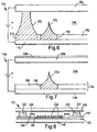
- FIG. 5 A cross-section of such grown tips 20i is shown in Figure 5 as is a cross-section of spacers 22i which have been formed by allowing the pulsed laser to rest upon certain areas of the thin film silicon to create line or dot crystalline structure (not shown) that have dimensions much bigger than those of the emitter dots (not shown). This results in a thicker deposited film being formed upon these crystalline areas.
- spacers 22i are grown at the time as the emitter tips 20i, allowing placement of gates for three terminal devices.
- the tips provide a sharp electron source that, when incorporated within a device 10, will provide hot electron injection into the light emitting layer of the device either through an evacuated space 24 or into a wide band-gap light emitting material 25.
- Each electron gains energy from the applied field, that is the field which is applied across the device 10 with aluminum substrate 12 acting as an electrode.
- the field emission device 10j is a vacuum device having grown spacers 22j on the micron scale.
- the substrate 14j is formed of aluminium onto which the thin film semiconductor based material 16j, in this case thin film hydrogenated amorphous silicon, is disposed by PECVD.
- a plurality of areas 18j, 21j of the hydrogenated amorphous silicon are crystallised by a laser interferometer and, using the growth and etch system, tips 20j and spacers 22j are grown.
- a plate of patterned Indium Tin Oxide (ITO) 26j, disposed on a glass substrate 28j, is arranged to sit on the grown spacers 22j of the emitter backplate 12j.
- the area 24j between the emitter tips 20j and the ITO 26j is evacuated.
- ITO Indium Tin Oxide
- FIG. 7 An alternative field emitting device 10k is shown in Figure 7.
- the field emitting device 10k is arranged with a wide band-gap light emitting material 25k, in this case a polymer, disposed on top of the field emission tips 20k for use as the light emitting medium.
- a diode configuration is fabricated with a thin film transparent metal such as Indium Tin Oxide (ITO) 26k disposed on a glass substrate 29k.
- ITO Indium Tin Oxide
- the device 10k has the field emission backplate 12k formed of silicon 16k disposed on a substrate 14k which in this case is aluminium.
- the thin film (in the order of many microns) of wide band-gap light emitting polymer 25k is disposed upon the plate of patterned ITO 26k on glass substrate 28k by, for example, screen printing.
- the light emitting polymer 25k is then pressed onto the crystalline silicon tips 20k of the backplate 12k.
- An Al-Si-polymer-ITO diode structure is thus formed with the polymer 25k being cured upon baking the device 10k to a temperature of approximately 100°C.
- Such a device arrangement is particularly useful in the case of the thin film semiconductor not being of n-type and there being no low barrier metal that enables electrons to be injected.
- a further alternative field emission device 101 including a metal coated phosphor layer member 301 disposed on a face plate 321, is shown in Figure 7.
- the device 101 is further adapted to form a triode configuration by the deposition of an insulator 341 with a metal gate 361 placed above.
- a yet further embodiment of a field emission backplate 12m involves constructing a three terminal device having self-aligned gates for each emitter 20m.
- This field emission backplate is constructed in a manner illustrated in Figures 9A - 9E.
- Figure 9A there is shown a backplate 12m formed of a substrate 14m, metal cathode 15m and a thin film of amorphous silicon 16m.
- the thin film silicon 16m is laser crystallised in the manner described with reference co Figures 1A-1F using an Nd:YAG laser with emission tips 20m formed by the crystallisation process as detailed previously.
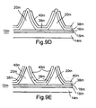
- the first step of forming the self aligned gates involves forming by deposition a chin SiN (Silicon Nitride) insulator 38m, using PEVCD, upon the exposed surface of crystallised silicon completely encapsulating each of the emitter tips 20m as is illustrated in Figure 9B.
- a chin SiN Silicon Nitride
- the second step of the process involves a layer of metal 40m, in this case chromium, being deposited on top of the SiN layer by thermal evaporation.
- the plate arrangement is then etched by plasma means, in this case using CF (freon) gas. This results in the top of each emitter tip losing its metal and the SiN insulator layer 38m being exposed as is shown in Figure 9D.
- the SiN insulator 38m is then etched leaving a supporting metal ring 41m around the exposed tip 20m which acts as a gate.
- the resultant emission backplate 12m which is shown in Figure 10A and in a close-up image in Figure 10B, can be used to form a field emission device 10m that is completely lithography free.
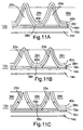
- this process can be improved by applying a planarising agent 37n, that is a liquid which upon heating or solvent evaporation becomes a thin planar film, to the crystallised backplate 12n after the second step of the process resulting in an arrangement as illustrated in Figure 11A.
- a planarising agent 37n that is a liquid which upon heating or solvent evaporation becomes a thin planar film
- the SiN insulator is then etched as before, leaving a space between the metal layer and the tip as is shown in Figure 11C.
- the planarising agent 37n in this way the underlying silicon backplate structure is protected from corrosive etch effects.
- the planarising agent can then be removed resulting in a metal gate surrounding each tip as shown in Figures 10A and 10B.
- Devices such as those detailed in the previous embodiments are suitable for many display applications due to their having low power consumption and being relatively simple to fabricate. Such devices may also be used as the cathodes for high power transistors for microwave amplifiers in the satellite and mobile communication markets.
- the process of crystallising the thin film amorphous silicon 16a - n has been described as being performed by a pulsed laser, however, this may also be performed by other means such as intense electron beam irradiation or high energy ion beam/particle impact or even thermal annealing.
- the depositing of the thin film of amorphous silicon 16a - m which may be intrinsic or doped n-type has been described by plasma enhanced chemical vapour deposition. However, the thin film may also be deposited by sputtering, evaporation or other such means.
- the substrate 14a - m on which the thin film silicon 16a - m has been deposited has been described as aluminum, however, may alternatively be metal such as molybdenum, chromium, or similar. It should be noted chat the electrode need not be formed integrally with the substrate 14a - m and may indeed be formed of a different material from the substrate 14a - m. Also the use of a Nd: YAG laser having 532nm wavelength chosen to maximise absorption in silicon is detailed, however, any other wavelength can be used and, in particular, other wavelengths to maximise absorption in other appropriate semiconductor based materials can be used. The use of a transparent metal to form a diode configuration field emission device is described, however, a suitable conducting polymer may alternatively be used.
- TFT control circuitry can be fabricated in the same manner as the described field emission backplate 12a - m either at pixel level or via integrated peripheral drivers.
- the chin film semiconductor in the detailed embodiments is an N-type hydrogenated amorphous silicon however the semiconductor may alternatively may be germanium or germanium alloy or similar.
- the substrate 14a - m on which the thin film semiconductor 16a - m is disposed has been detailed as being aluminium however may be formed of various other types of metal such as mobidium, chromium or similar.
- the use of a KrF (Krypton Fluorine) excimer laser is described however any excimer laser may be used.
- each embodiment of the device 10a - m may be adapted to form a triode configuration by the deposition of an insulator 34a - m with a metal gate 36a - m placed above.
- the silicon backplate described with reference to Figure 9 is detailed as being crystallised using a Nd:YAG laser, however, it may be crystallised using an excimer laser and may be crystallised using a laser interferometry technique.
- the insulator 38m disposed on the crystallised silicon 16m is described as being SiN however it may be any suitable insulator and may be deposited using any conformal coating method.
- the layer of metal 40m disposed upon the insulator has been described as being deposited using thermal evaporation, however, sputtering or any other suitable technique may be used.
Landscapes
- Engineering & Computer Science (AREA)
- Manufacturing & Machinery (AREA)
- Cold Cathode And The Manufacture (AREA)
- Cathode-Ray Tubes And Fluorescent Screens For Display (AREA)
- Electrodes For Cathode-Ray Tubes (AREA)
- Recrystallisation Techniques (AREA)
- Gas-Filled Discharge Tubes (AREA)
Abstract
Description
- The present invention relates to a field emission backplate and to a related arrangement and method of manufacture. In particular, though not exclusively, the invention relates to a field emission backplate comprising a plurality of emission sites or "silicon tips" formed by laser crystallisation and selective regrowth. The invention finds use in displays.
- Flat panel displays are of immense importance in electronics. In current developments, Active Matrix Liquid Crystal Displays (AMLCD) are beginning to challenge the dominance of Cathode Ray Tube (CRT) technology. AMLCD devices are non-emissive and require complex lithography. Filters and matching spectral backlights are required to produce colour. However, there are many light losses and inherent complexity in AMLCD devices because of the nonlinear nature of liquid crystal materials. This results in a display that is less bright than CRT with a smaller colour gamut and poorer viewing angle and contrast. Also, due to the non-emissive nature of the display, inefficient use of input electrical power is made often with well over 70% of the energy being lost as non-useful energy.
- Field emission displays, based on conventional 'Spindt Tip' technology, promised a solution to flat panel display problems. Field emission displays (FEDs) are essentially flat cathode ray tube (CRT) devices. However, rather than one electron gun firing electrons at a phosphor on a screen through a shadow mask, the FED has tens or hundreds of individual rips in each display pixel. The tips are known as Spindt tips, after the inventor Cap Spindt. The process of fabrication relies on defining a pattern of holes in a gate metal by photolithography. An underlying insulator is then etched in an isotropic wet etch that "undercuts" leaving a well beneath the metal. A sacrificial layer (usually nickel) is then evaporated on the surface at an oblique angle to ensure the well is not filled. The emitter material (usually tungsten or molybdenum) is then evaporated through the holes in to the well. As the evaporate metal builds up on the surface, on the sacrificial layer, it closes the hole as the thickness increases, and has the effect of providing an emitter tip in the well. The top metal is then removed by etching the sacrificial layer, leaving the tip, the well, and the original gate metal. This forms the backplate of Spindt tips. A top plate containing a patterned phosphor is then placed relative to the backplate using spacers. The final device is evacuated to allow the emitted electrons a long mean free path. The principle of field emission from micro-tips is well understood and is governed by Fowler - Nordheim tunnelling. The emission current, and therefore brightness of the display, depends then only on the current density, the number of tips and their sharpness, i.e.

- The tips will provide a sharp electron source that will provide hot electron injection into, for example, a phosphor.
- Unfortunately, the extreme complication in fabrication has limited the use of this technology. Additionally, crystal silicon emitters are limited by the wafer size.
- Other thin-film materials may also be used for field emission. Carbon is the main contender with diamond, diamond like carbon and carbon nano-tubes also suitable. The use of diamond seemed a good choice, although this is difficult to fabricate and also the mechanism of a supposed negative electron affinity which diamond was claimed to have has now been questioned.
- An object of at least one embodiment of at least one aspect of the present invention is to obviate or at least mitigate at least one of the aforementioned problems in the prior art.
- According to a first aspect of the present invention there is provided a method of forming a field emission backplate comprising:
- providing a planar body of amorphous semiconductor based material upon a substrate; and
- laser crystallising at least a portion of the amorphous semiconductor based material;
- Preferably the planar body of amorphous semiconductor based material is provided by depositing a thin film of the material upon a substrate.
- Conveniently, the semiconductor based material is silicon or an alloy thereof.
- Preferably the laser crystallising is performed using an excimer laser or Nd:YAG laser.
- Conveniently, the excimer laser is a KrF laser.
- It will be understood that in the context of the present invention the term "thin film" is used to define a film of a few nanometers, for example, 1 to 100nm, and typically 10nm.
- According to a second aspect of the invention there is provided a field emission backplate comprising a plurality of emitter sites formed by laser crystallisation of a thin film of amorphous semiconductor based material.
- Conveniently, the semiconductor based material is silicon or an alloy thereof.
- According to a third aspect of the invention there is provided a field emission device comprising a field emission backplate having a plurality of emitter sites formed by laser crystallising of a thin film of amorphous semiconductor based material.
- The field emission device may be a vacuum device wherein the emitter sites of the backplate act as an emission sources in the device.
- Conveniently, the field emission device comprises a substrate, a field emission backplate, and an evacuated space and a transparent window, e.g. thin film transparent metal or metallised phosphor, wherein the field emission backplate is formed upon the substrate and the evacuated space is located between the field emission backplate and the thin film transparent metal or metallised phosphor.
- Alternatively, the field emission device comprises a wide band-gap light emitting material, eg light emitting polymer into which electrons from the emitter sites of the backplate are emitted.
- Conveniently, the field emission device comprises a substrate, a field emission backplate, on one side of which is formed a plurality of emitter sites, a light emitting polymer and a thin film transparent metal or metallised phosphor wherein the field emission backplate is formed upon the substrate, one surface of the light emitting polymer is disposed on the plurality of emitter sites of the field emission backplate, the thin film transparent metal being disposed on the other surface of the light emitting polymer.
- Conveniently, the field emission device is a display device.
- According to a fourth aspect of the present invention there is provided a field emission backplate comprising a plurality of grown tips, the backplate being made substantially from semiconductor based material.
- Preferably the plurality of tips are formed on a thin film of semiconductor based material.
- Preferably the grown tips are "profiled", that is to say grown in a manner resulting in a sharp pointed shape.
- Conveniently, the tips are grown and etched simultaneously.
- Conveniently, the semiconductor based material is silicon or an alloy thereof.
- According to a fifth aspect of the present invention there is provided a field emission backplate comprising a planar member of substantially amorphous material and a plurality of tips of crystalline material thereon.
- Preferably the tips are formed on crystalline or crystallised areas of the planar member.
- According to a sixth aspect of the invention there is provided a field emission backplate comprising a plurality of grown tips, the backplate being made substantially from a thin film silicon based material.
- Preferably the plurality of tips are formed by the growth of crystalline silicon on a plurality of crystallized areas of the thin film of amorphous silicon.
- According to a seventh aspect of the invention there is provided a field emission device having a backplate comprising an array of (profiled) tips formed by the selective growth of crystalline semiconductor based material on a plurality of crystallized areas of a thin film of amorphous semiconductor based material.
- The field emission device may be a vacuum device wherein the emitter tips of the backplate act as an emission source in the device.
- Conveniently, the field emission device comprises a substrate, a field emission backplate, an evacuated space and a transparent window, e.g. thin film transparent metal, wherein the field emission backplate is formed upon the substrate and the evacuated space is located between the field emitting backplate and the thin film transparent metal.
- Alternatively, the field emission device may comprises a wide band-gap light emitting material, e.g. light emitting polymer into which electrons from the emitter tips of the backplate are emitted in use.
- Conveniently, the field emission device comprises a substrate, a field emission backplate, on one side of which is formed a plurality of tips, a light emitting polymer and a thin film transparent metal wherein the field emission backplate is formed upon the substrate, one surface of the light emitting polymer is disposed on the plurality of tips of the field emission backplate, the thin film transparent metal be disposed on the other surface of the light emitting polymer.
- Conveniently the field emission device is a display device.
- Preferably, the tips of the field emission backplate of the display device are of a density of at least 100 per square micron.
- According to an eighth aspect of the invention there is provided a method of forming a field emission backplate comprising:
- depositing a thin film of amorphous semiconductor based material upon a substrate;
- locally crystallizing a plurality of areas of the thin film amorphous semiconductor based material; and
- growing crystalline semiconductor based material upon each of the plurality of crystallized areas cf thin film amorphous semiconductor based material.
- Conveniently the thin film of amorphous semiconductor based material is deposited on a substrate e.g. by plasma enhanced chemical vapour deposition (PECVD).
- Preferably the plurality of areas of thin film amorphous semiconductor based material are crystallized by exposure to at least one pulse of a laser interference pattern.
- According to a ninth aspect of the invention there is provided a method of crystallizing areas of thin film amorphous semiconductor based material for use in a field emission backplate comprising:
- forming a laser interferometer by splitting and recombining a laser beam;
- placing the thin film of amorphous semiconductor based material in a plane of recombination of the laser beam;
- locally crystallizing areas of the thin film of amorphous semiconductor based material by subjecting the thin film to at least one laser pulse, wherein the crystallised areas generated in the thin film amorphous semiconductor based material correspond to the interference pattern of the laser.
- Preferably, tor a backplate of amorphous semiconductor based material wherein the semiconductor based material is hydrogenated amorphous silicon, the laser operates at a wavelength of around 532nm to maximise absorption and preferably the laser is a Nd:YAG laser.
- These and other aspects of the invention will become apparent from the following description when taken in combination with the accompanying drawings which show:
- Figures 1A - 1F
- a thin film semiconductor crystallised at various energies according to the present invention;
- Figure 2
- a field emission device according to a first embodiment of the present invention;
- Figure 3
- a graph of field emission current vs electric field for a field emission backplate of the field emission device of Figure 2;
- Figure 4
- a schematic perspective view of a thin film of amorphous silicon onto which is projected a laser interference pattern in forming a field emission backplate;
- Figure 5
- a cross-section of a side profile of a grown crystalline silicon backplate according to a second embodiment of the present invention;
- Figure 6
- a schematic side view of a field emission device having crystalline silicon tips according to a third embodiment of the present invention;
- Figure 7
- a schematic side view of a field emission device having crystalline silicon tips according to a fourth embodiment of the present invention;
- Figure 8
- a schematic side view of a field emission device having crystalline silicon tips according to a fifth embodiment of the present invention;
- Figures 9A - 9E
- a series of side cross-sectioned views showing a method of forming a field emission backplate according to a sixth embodiment of the present invention;
- Figures 10A & 10B
- photographic images of the field emission backplate of Figures 9A - 9E;
- Figures 11A - 11C
- a series of side cross-sectional views showing a method of forming a field emission backplate formed according to a seventh embodiment of the present invention including the use of a planarising agent.
- With reference initially to Figures 1A - 1F there is shown photographic images of
field emission backplates 12a to 12f each formed of an amorphous semiconductor based material, in this case n-type hydrogenated amorphous silicon, on the surface of which a plurality ofemitter sites 20a-20f are formed. Thefield emission backplate 12a - 12f is formed by the deposition of a thin film of approximately 100nm of n-type hydrogenated amorphous silicon onto a substrate of, for example, aluminium by plasma enhanced chemical vapour deposition (PECVD). The deposited thin film then undergoes laser crystallisation by an excimer laser or Nd:YAG laser, in this case a KrF laser operating at a wavelength of 248nm scanning at 2mm\s in an atmosphere of oxygen and then quenched. Alternatively a Nd:YAG laser operating at a wavelength of 532nm is used. The laser is pulsed at 3 to 7 nanoseconds and stepped and repeated to form a pattern. This process results in the surface of the silicon having a rough texture. The energy absorbed by the silicon influences the extent of roughening of the surface as can be seen in Figures 1A - 1F, with Figure 1A showing theemitter tips 20a which are the resultant effect of a small amount of absorbed energy i.e. approximately 100 mJ\cm-. This can be compared to Figure 1F which shows therounded emitter tips 20f achieved by a relatively large amount absorbed energy, in the region of 300 mJ\cm. In each case, each of thetips 20a - 20f acts as an emitter site. When thebackplate 12 is incorporated in a field emission device (not shown), eachemitter site 20a - 20f emits electrons at low fields in a field emission configuration. Thebackplate 12a - 12f results in emission currents in excess of 10-5 A and low field threshold of around 10V/µm. - An example first embodiment
field emission device 10g, having a field emission backplate 12g formed as described with reference to Figures 1A - 1F, is shown in Figure 2. Thedevice 10g shown is a triode device having a field emission backplate 12g with asubstrate 14g of aluminium and athin film 16g of n-type hydrogenated amorphous silicon which has been treated by an excimer laser and.thus has a plurality ofemitter sites 20g upon the surface. An insulating layer, for example, a layer of an insulating material such as silicon nitride, has been disposed on the crystallised silicon, and subsequently etched thus providingspacer elements 22g. Upon each of thesespacer elements 22g is disposed athin film 26g of phosphor, e.g. metallised phosphor and the device is completed with a layer ofglass 28g thus giving a three terminal gate control arrangement. The area 24g between theglass 28g and theemitter sites 20g is evacuated which allows the emission to be controlled using low voltages and this is important for effective spacial control when thedevice 10g is used in display arrangements. - Emission currents measured in such a
device 10g having a vacuum below 5 x 10- mbars are shown in Figure 3 which is a graphical representation of the emission current vs the electric field. It is also estimated that the beta factor for the describeddevice 10g is in excess of 450 with this figure including both geometric enhancement and internal enhancement. - In Figure 4, there is shown a thin film of
amorphous silicon 16h disposed upon a substrate ofaluminum 14h wherein a pattern ofdots 18h caused by a laser interference pattern can be seen upon a region of surface of thesilicon 16h. This arrangement illustrates a refinement of the technique used to form a backplate such as that of the first embodiment, the technique being used to produce a field emission backplate. - The thin film of
amorphous silicon 16h is disposed upon the substrate ofaluminum 14h by plasma enhanced chemical vapour deposition (PECVD). A Nd:YAG pulse laser, having a pulsing duration in the region of 3 to 7 nanoseconds, is used to form an interferometer, with the beam being split and brought back together forming a pattern ofdots 18h. The thinfilm silicon layer 16h is positioned in a plane in which the interference pattern of the laser is formed. The laser interference pattern acts upon thesilicon layer 16h creating areas, ordots 18h, of crystallisation. A single pulse of an Nd:YAG laser is used r.o locally crystallize the region. The laser beam is synchronised with a step and repeat system in the plane of thethin film silicon 16h resulting in the formation of laser spots, and hence the crystalliseddots 18h, distributed over the entire surface plate of thethin film silicon 16h, thus allowing a high density of tips to be made. By using this step and repeat system thebackplate 12h may be made of any chosen size. An area of 30µm x 30µm is typical for an individual pixel, and hence a micro tip density of 300 x 300, which equals 9 x 10⁴ per Red Green Blue (RGB) pixel will be achieved. Such density of emitters is of crucial importance as the emission current of a field emission device depends on the number of tips and their sharpness. - A selective etch and growth process involving a dilute silane/hydrogen plasma forms micro crystalline silicon by allowing strained bonds within a silicon array, to be broken by the mobile hydrogen while deposited silicon atoms form thermodynamically stable crystalline sites. To form emitter tips 20h upon the laser treated
thin film silicon 16h, resulting in a cross-section of tips 20h such as those shown in Figure 5, the PECVD depositedthin film silicon 16h is subjected to a dilute silane/hydrogen plasma in a reactor. - During this process, deposition of silicon atoms will only take place on a crystalline substrate and therefore in this case upon the crystallised
dots 18h of thethin film silicon 16h. Amorphous or weak bonded areas of the structure are simultaneously etched. Continued growth has the effect of profiling the edges of the growing film where the etching effect is more dramatic. As eachcrystalline area 18h is limited in size to less than 100nm, the aspect ratio is such that the edges converge. Therefore, eachcircular dot 18h of 100nm or less of theemitter plate 12h effectively grows d profile tip 20h. The growth and etching processes are mediated by mobile hydrogen and the aspect ratio profiling etching leading to sharp tips 20h over the entire growing surface of the plate ofthin film silicon 16h. This profiling leads to field enhancement of theemission plate 12h which therefore gives a low threshold (of around 15v/µm) for field emission and thus higher emission current (i.e. in excess of 10-4 amps) than that achievable with the field emission backplate of the first embodiment. - A cross-section of such
grown tips 20i is shown in Figure 5 as is a cross-section ofspacers 22i which have been formed by allowing the pulsed laser to rest upon certain areas of the thin film silicon to create line or dot crystalline structure (not shown) that have dimensions much bigger than those of the emitter dots (not shown). This results in a thicker deposited film being formed upon these crystalline areas. Thusspacers 22i are grown at the time as theemitter tips 20i, allowing placement of gates for three terminal devices. - As the emission current, and therefore the brightness of the display depends upon the current density, the number of tips, and their sharpness, according to I=JSN nα. The tips provide a sharp electron source that, when incorporated within a
device 10, will provide hot electron injection into the light emitting layer of the device either through an evacuated space 24 or into a wide band-gaplight emitting material 25. Each electron gains energy from the applied field, that is the field which is applied across thedevice 10 withaluminum substrate 12 acting as an electrode. - A field
emission device configuration 10j having crystallisedsilicon emitter tips 20j formed as described with reference to figures 4 and 5 is shown in Figure 6. - The
field emission device 10j is a vacuum device having grownspacers 22j on the micron scale. Thesubstrate 14j is formed of aluminium onto which the thin film semiconductor basedmaterial 16j, in this case thin film hydrogenated amorphous silicon, is disposed by PECVD. As has been detailed previously, a plurality ofareas tips 20j andspacers 22j are grown. A plate of patterned Indium Tin Oxide (ITO) 26j, disposed on a glass substrate 28j, is arranged to sit on the grownspacers 22j of the emitter backplate 12j. Thearea 24j between theemitter tips 20j and theITO 26j is evacuated. - An alternative
field emitting device 10k is shown in Figure 7. In this configuration thefield emitting device 10k is arranged with a wide band-gaplight emitting material 25k, in this case a polymer, disposed on top of thefield emission tips 20k for use as the light emitting medium. A diode configuration is fabricated with a thin film transparent metal such as Indium Tin Oxide (ITO) 26k disposed on a glass substrate 29k. Thedevice 10k has thefield emission backplate 12k formed ofsilicon 16k disposed on asubstrate 14k which in this case is aluminium. The thin film (in the order of many microns) of wide band-gaplight emitting polymer 25k is disposed upon the plate ofpatterned ITO 26k onglass substrate 28k by, for example, screen printing. Thelight emitting polymer 25k is then pressed onto thecrystalline silicon tips 20k of thebackplate 12k. An Al-Si-polymer-ITO diode structure is thus formed with thepolymer 25k being cured upon baking thedevice 10k to a temperature of approximately 100°C. Such a device arrangement is particularly useful in the case of the thin film semiconductor not being of n-type and there being no low barrier metal that enables electrons to be injected. - A further alternative
field emission device 101, including a metal coatedphosphor layer member 301 disposed on aface plate 321, is shown in Figure 7. Thedevice 101 is further adapted to form a triode configuration by the deposition of aninsulator 341 with ametal gate 361 placed above. - A yet further embodiment of a
field emission backplate 12m involves constructing a three terminal device having self-aligned gates for eachemitter 20m. This field emission backplate is constructed in a manner illustrated in Figures 9A - 9E. In Figure 9A there is shown abackplate 12m formed of asubstrate 14m,metal cathode 15m and a thin film ofamorphous silicon 16m. Thethin film silicon 16m is laser crystallised in the manner described with reference co Figures 1A-1F using an Nd:YAG laser withemission tips 20m formed by the crystallisation process as detailed previously. - The first step of forming the self aligned gates involves forming by deposition a chin SiN (Silicon Nitride)
insulator 38m, using PEVCD, upon the exposed surface of crystallised silicon completely encapsulating each of theemitter tips 20m as is illustrated in Figure 9B. - The second step of the process, the results of which are shown in Figure 9C, involves a layer of
metal 40m, in this case chromium, being deposited on top of the SiN layer by thermal evaporation. - In the third step of the process, the plate arrangement is then etched by plasma means, in this case using CF (freon) gas. This results in the top of each emitter tip losing its metal and the
SiN insulator layer 38m being exposed as is shown in Figure 9D. - As is shown in Figure 9E, the
SiN insulator 38m is then etched leaving a supportingmetal ring 41m around the exposedtip 20m which acts as a gate. - The
resultant emission backplate 12m, which is shown in Figure 10A and in a close-up image in Figure 10B, can be used to form a field emission device 10m that is completely lithography free. - Referring to Figures 11A - 11C, this process can be improved by applying a planarising agent 37n, that is a liquid which upon heating or solvent evaporation becomes a thin planar film, to the crystallised
backplate 12n after the second step of the process resulting in an arrangement as illustrated in Figure 11A. This shows the planarising agent 37n coating thebackplate 12n leaving theemitter tips 20n standing proud. - The step of etching the arrangement by plasma means thus results in the arrangement shown in Figure 11B.
- The SiN insulator is then etched as before, leaving a space between the metal layer and the tip as is shown in Figure 11C. By utilising the planarising agent 37n in this way the underlying silicon backplate structure is protected from corrosive etch effects. The planarising agent can then be removed resulting in a metal gate surrounding each tip as shown in Figures 10A and 10B.
- Devices such as those detailed in the previous embodiments are suitable for many display applications due to their having low power consumption and being relatively simple to fabricate. Such devices may also be used as the cathodes for high power transistors for microwave amplifiers in the satellite and mobile communication markets.
- Various modifications may be made to the embodiment of the invention as hereinbefore described without departing from the scope of the invention. For example, during the laser treatment of the thin film amorphous silicon 16a - m, the use of a single laser pulse has been described in locally crystallising the region, however, a number of pulses may alternatively be used thus allowing energies as low as 20mJcm- to be used. Additionally, it has been described how the crystallisation of larger line or dot structures 21a - m can be used to grow spacers 22a - n during the selective each and growth process of the
tips 20a - m, however, silicon can also be grown in blocks on an insulator and thin film transistor devices for active address delineated in the same process. - The process of crystallising the thin film amorphous silicon 16a - n has been described as being performed by a pulsed laser, however, this may also be performed by other means such as intense electron beam irradiation or high energy ion beam/particle impact or even thermal annealing.
- The depositing of the thin film of amorphous silicon 16a - m which may be intrinsic or doped n-type has been described by plasma enhanced chemical vapour deposition. However, the thin film may also be deposited by sputtering, evaporation or other such means.
- The substrate 14a - m on which the thin film silicon 16a - m has been deposited has been described as aluminum, however, may alternatively be metal such as molybdenum, chromium, or similar. It should be noted chat the electrode need not be formed integrally with the substrate 14a - m and may indeed be formed of a different material from the substrate 14a - m. Also the use of a Nd: YAG laser having 532nm wavelength chosen to maximise absorption in silicon is detailed, however, any other wavelength can be used and, in particular, other wavelengths to maximise absorption in other appropriate semiconductor based materials can be used. The use of a transparent metal to form a diode configuration field emission device is described, however, a suitable conducting polymer may alternatively be used.
- Furthermore TFT control circuitry can be fabricated in the same manner as the described
field emission backplate 12a - m either at pixel level or via integrated peripheral drivers. - The chin film semiconductor in the detailed embodiments is an N-type hydrogenated amorphous silicon however the semiconductor may alternatively may be germanium or germanium alloy or similar. The substrate 14a - m on which the thin film semiconductor 16a - m is disposed has been detailed as being aluminium however may be formed of various other types of metal such as mobidium, chromium or similar. The use of a KrF (Krypton Fluorine) excimer laser is described however any excimer laser may be used.
- The device described in Figure 8 is detailed as including a metal coated
phosphor layer 301 disposed on aface plate 321, however, it should be understood that the other device embodiments detailed may also include this feature. Furthermore, each embodiment of the device 10a - m may be adapted to form a triode configuration by the deposition of an insulator 34a - m with a metal gate 36a - m placed above. - The silicon backplate described with reference to Figure 9 is detailed as being crystallised using a Nd:YAG laser, however, it may be crystallised using an excimer laser and may be crystallised using a laser interferometry technique. Furthermore, the
insulator 38m disposed on the crystallisedsilicon 16m is described as being SiN however it may be any suitable insulator and may be deposited using any conformal coating method. The layer ofmetal 40m disposed upon the insulator has been described as being deposited using thermal evaporation, however, sputtering or any other suitable technique may be used.
Claims (13)
- A method of forming a field emission backplate (12a - 12f; 12g; 12k) comprising:providing a planar body of amorphous semiconductor based material upon a substrate (14g; 14h; 14j); andlaser crystallising at least a portion of the amorphous semiconductor based material;wherein upon crystallising the amorphous semiconductor based material a plurality of emitter sites (20a - 20f; 20g; 20i; 20h) are formed.
- A method as claimed in claim 1, wherein the planar body of amorphous semiconductor based material is provided by depositing a thin film (16g; 16h) of material upon a substrate (14g; 14h; 14j).
- A method as claimed in either of claims 1 or 2, wherein the semiconductor based material is silicon or an alloy thereof.
- A method as claimed in claim 2, further comprising the step of performing laser crystallising using an excimer laser or Nd:YAG laser.
- A method as claimed in claim 4, wherein the excimer laser is a KrF laser.
- A field emission backplate (12a - 12f; 12g; 12k) comprising a plurality of emitter sites (20a - 20f; 20g; 20i; 20j) formed by laser crystallisation of a planar body or thin film (16g; 16h) of amorphous semiconductor based material.
- A field emission backplate as claimed in claim 6, wherein the semiconductor based material is silicon or an alloy thereof.
- A field emission device (10g; 10j; 10k; 10l) comprising a field emission backplate (12a - 12f; 12g; 12k) comprising a plurality of emitter sites (20a - 20f; 20g; 20i; 20j) formed by laser crystallising of a planar body or thin film (16g; 16h) of amorphous semiconductor based material.
- A field emission device as claimed in claim 8, wherein the field emission device is a vacuum device, wherein the emitter sites of the backplate act as emission sources in the device, in use.
- A field emission device as claimed in claim 9, further comprising a substrate (14g; 14h; 14j), an evacuated space (24) and a transparent window (26g), wherein the field emission backplate is formed upon the substrate and the evacuated space is located between the field emission backplate and the transparent window.
- A field emission device as claimed in claim 8, further comprising a wide band-gap light emitting material (25; 25k) into which electrons from the emitter sites of the backplate are emitted, in use.
- A field emission device as claimed in claim 11, comprising a substrate, the field emission backplate on one side of which is formed the plurality of emitter sites, the wide band-gap light emitting material comprising a light emitting polymer, and a transparent window comprising a thin film transparent metal or metallised phosphor, wherein the field emission backplate is formed upon the substrate, and one surface of the light emitting polymer is disposed on the plurality of emitter sites of the field emission backplate, the transparent window being disposed on another surface of the light emitting polymer.
- A field emission device as claimed in any of claims 8 to 12, wherein the device is a display device.
Applications Claiming Priority (5)
| Application Number | Priority Date | Filing Date | Title |
|---|---|---|---|
| GB0119657 | 2001-08-11 | ||
| GB0119659 | 2001-08-11 | ||
| GB0119657A GB2378569B (en) | 2001-08-11 | 2001-08-11 | Improved field emission backplate |
| GB0119659A GB2378570B (en) | 2001-08-11 | 2001-08-11 | Improved field emission backplate |
| PCT/GB2002/003691 WO2003015117A1 (en) | 2001-08-11 | 2002-08-09 | Field emission backplate |
Publications (2)
| Publication Number | Publication Date |
|---|---|
| EP1417695A1 EP1417695A1 (en) | 2004-05-12 |
| EP1417695B1 true EP1417695B1 (en) | 2008-01-23 |
Family
ID=26246435
Family Applications (1)
| Application Number | Title | Priority Date | Filing Date |
|---|---|---|---|
| EP02751413A Expired - Lifetime EP1417695B1 (en) | 2001-08-11 | 2002-08-09 | Field emission backplate |
Country Status (8)
| Country | Link |
|---|---|
| US (1) | US7592191B2 (en) |
| EP (1) | EP1417695B1 (en) |
| JP (1) | JP4532108B2 (en) |
| KR (1) | KR100730808B1 (en) |
| CN (1) | CN1639820B (en) |
| AT (1) | ATE385038T1 (en) |
| DE (1) | DE60224808T2 (en) |
| WO (1) | WO2003015117A1 (en) |
Families Citing this family (9)
| Publication number | Priority date | Publication date | Assignee | Title |
|---|---|---|---|---|
| JP4532108B2 (en) * | 2001-08-11 | 2010-08-25 | ザ・ユニバーシティ・コート・オブ・ザ・ユニバーシティ・オブ・ダンディ | Field emission back plate, field emission device using the field emission back plate, and method for manufacturing the field emission back plate |
| US7015496B2 (en) * | 2002-12-27 | 2006-03-21 | Semiconductor Energy Laboratory Co., Ltd. | Field emission device and manufacturing method thereof |
| US7674149B2 (en) * | 2005-04-21 | 2010-03-09 | Industrial Technology Research Institute | Method for fabricating field emitters by using laser-induced re-crystallization |
| KR100787630B1 (en) * | 2006-05-24 | 2007-12-21 | 경희대학교 산학협력단 | Display element and manufacturing method thereof |
| TW200816266A (en) * | 2006-09-22 | 2008-04-01 | Innolux Display Corp | Field emission display and method of fabricating the same |
| CN101381492B (en) * | 2007-09-06 | 2011-07-06 | 比亚迪股份有限公司 | A kind of composite polypropylene material and preparation method thereof |
| GB0722120D0 (en) * | 2007-11-10 | 2007-12-19 | Quantum Filament Technologies | Improved field emission backplate |
| KR101610260B1 (en) * | 2008-12-15 | 2016-04-08 | 삼성전자주식회사 | Electron beam anneling apparatus and annealing method using the same |
| CN106744659B (en) * | 2016-12-13 | 2018-09-07 | 杭州电子科技大学 | Research method based on laser controlling nanostructure silicon substrate surface form |
Family Cites Families (31)
| Publication number | Priority date | Publication date | Assignee | Title |
|---|---|---|---|---|
| DE68913419T2 (en) | 1988-03-25 | 1994-06-01 | Thomson Csf | METHOD FOR PRODUCING FIELD EMISSION ELECTRON SOURCES AND APPLICATION FOR PRODUCING EMITTER MATRICES. |
| JPH01290598A (en) | 1988-05-17 | 1989-11-22 | Res Dev Corp Of Japan | Production of fine multiprobe |
| JPH05274998A (en) * | 1992-03-23 | 1993-10-22 | Shimadzu Corp | Electron emission element |
| US5329207A (en) * | 1992-05-13 | 1994-07-12 | Micron Technology, Inc. | Field emission structures produced on macro-grain polysilicon substrates |
| JP3267418B2 (en) | 1993-06-25 | 2002-03-18 | 双葉電子工業株式会社 | Field emission cathode device |
| US5804919A (en) * | 1994-07-20 | 1998-09-08 | University Of Georgia Research Foundation, Inc. | Resonant microcavity display |
| JP3239285B2 (en) | 1993-11-22 | 2001-12-17 | 双葉電子工業株式会社 | Method of manufacturing field emission cathode |
| RU2074444C1 (en) | 1994-07-26 | 1997-02-27 | Евгений Инвиевич Гиваргизов | Self-emitting cathode and device which uses it |
| US5804910A (en) * | 1996-01-18 | 1998-09-08 | Micron Display Technology, Inc. | Field emission displays with low function emitters and method of making low work function emitters |
| TW472273B (en) * | 1999-04-23 | 2002-01-11 | Matsushita Electric Works Ltd | Field emission-type electron source and manufacturing method thereof |
| US6765342B1 (en) * | 1999-10-18 | 2004-07-20 | Matsushita Electric Work, Ltd. | Field emission-type electron source and manufacturing method thereof |
| US6451631B1 (en) * | 2000-08-10 | 2002-09-17 | Hitachi America, Ltd. | Thin film crystal growth by laser annealing |
| US6572425B2 (en) | 2001-03-28 | 2003-06-03 | Intel Corporation | Methods for forming microtips in a field emission device |
| GB2378570B (en) | 2001-08-11 | 2005-11-16 | Univ Dundee | Improved field emission backplate |
| JP4532108B2 (en) * | 2001-08-11 | 2010-08-25 | ザ・ユニバーシティ・コート・オブ・ザ・ユニバーシティ・オブ・ダンディ | Field emission back plate, field emission device using the field emission back plate, and method for manufacturing the field emission back plate |
| GB2378569B (en) | 2001-08-11 | 2006-03-22 | Univ Dundee | Improved field emission backplate |
| GB2389959B (en) * | 2002-06-19 | 2006-06-14 | Univ Dundee | Improved field emission device |
| US7247527B2 (en) * | 2003-07-31 | 2007-07-24 | Semiconductor Energy Laboratory Co., Ltd. | Method for manufacturing semiconductor device, and laser irradiation apparatus |
| US7358165B2 (en) * | 2003-07-31 | 2008-04-15 | Semiconductor Energy Laboratory Co., Ltd | Semiconductor device and method for manufacturing semiconductor device |
| KR101188356B1 (en) * | 2003-12-02 | 2012-10-08 | 가부시키가이샤 한도오따이 에네루기 켄큐쇼 | Laser irradiation apparatus, laser irradiation method, and method for manufacturing semiconductor device |
| EP1553643A3 (en) * | 2003-12-26 | 2009-01-21 | Sel Semiconductor Energy Laboratory Co., Ltd. | Laser irradiation method and method for manufacturing crystalline semiconductor film |
| JP2007078350A (en) | 2004-02-17 | 2007-03-29 | Masao Yoshida | Method of manufacturing reference gauge used for inspection of flaw |
| US7902002B2 (en) * | 2004-07-30 | 2011-03-08 | Semiconductor Energy Laboratory Co., Ltd. | Semiconductor device |
| US7674149B2 (en) * | 2005-04-21 | 2010-03-09 | Industrial Technology Research Institute | Method for fabricating field emitters by using laser-induced re-crystallization |
| DE602006004913D1 (en) * | 2005-04-28 | 2009-03-12 | Semiconductor Energy Lab | Method and device for producing semiconductors by means of laser radiation |
| WO2007139210A1 (en) * | 2006-05-31 | 2007-12-06 | Semiconductor Energy Laboratory Co., Ltd. | Display device |
| CN101479777B (en) * | 2006-05-31 | 2011-07-06 | 株式会社半导体能源研究所 | Display devices and electronics |
| TWI412079B (en) * | 2006-07-28 | 2013-10-11 | 半導體能源研究所股份有限公司 | Method of manufacturing a display device |
| KR101346246B1 (en) * | 2006-08-24 | 2013-12-31 | 가부시키가이샤 한도오따이 에네루기 켄큐쇼 | Method for manufacturing display device |
| TW200816266A (en) * | 2006-09-22 | 2008-04-01 | Innolux Display Corp | Field emission display and method of fabricating the same |
| WO2008069219A1 (en) * | 2006-12-05 | 2008-06-12 | Semiconductor Energy Laboratory Co., Ltd. | Antireflective film and display device |
-
2002
- 2002-08-09 JP JP2003519955A patent/JP4532108B2/en not_active Expired - Fee Related
- 2002-08-09 DE DE60224808T patent/DE60224808T2/en not_active Expired - Fee Related
- 2002-08-09 KR KR1020047002038A patent/KR100730808B1/en not_active Expired - Fee Related
- 2002-08-09 WO PCT/GB2002/003691 patent/WO2003015117A1/en not_active Ceased
- 2002-08-09 AT AT02751413T patent/ATE385038T1/en not_active IP Right Cessation
- 2002-08-09 EP EP02751413A patent/EP1417695B1/en not_active Expired - Lifetime
- 2002-08-09 CN CN028157605A patent/CN1639820B/en not_active Expired - Fee Related
-
2004
- 2004-02-06 US US10/773,696 patent/US7592191B2/en not_active Expired - Fee Related
Also Published As
| Publication number | Publication date |
|---|---|
| KR100730808B1 (en) | 2007-06-20 |
| JP2005505101A (en) | 2005-02-17 |
| DE60224808D1 (en) | 2008-03-13 |
| ATE385038T1 (en) | 2008-02-15 |
| CN1639820A (en) | 2005-07-13 |
| CN1639820B (en) | 2010-05-26 |
| US20040197942A1 (en) | 2004-10-07 |
| DE60224808T2 (en) | 2009-02-05 |
| EP1417695A1 (en) | 2004-05-12 |
| KR20040030956A (en) | 2004-04-09 |
| WO2003015117A1 (en) | 2003-02-20 |
| US7592191B2 (en) | 2009-09-22 |
| HK1077919A1 (en) | 2006-02-24 |
| JP4532108B2 (en) | 2010-08-25 |
Similar Documents
| Publication | Publication Date | Title |
|---|---|---|
| US5232549A (en) | Spacers for field emission display fabricated via self-aligned high energy ablation | |
| CN100490047C (en) | Field emission device and manufacture method thereof | |
| US6426234B2 (en) | Method of making field emitters using porous silicon | |
| CN100501498C (en) | Field emission device and method for forming field emission device | |
| US7592191B2 (en) | Field emission backplate | |
| JP2987140B2 (en) | Field emission electron source, method of manufacturing the same, flat light emitting device, display device, and solid-state vacuum device | |
| GB2378569A (en) | Field emission backplate and device | |
| JP3239285B2 (en) | Method of manufacturing field emission cathode | |
| HK1077919B (en) | Field emission backplate | |
| JP3406895B2 (en) | Field emission cold cathode device, method of manufacturing the same, and vacuum micro device | |
| JPH09129123A (en) | Electron emitting device and method of manufacturing the same | |
| WO2008017809A1 (en) | Field emission backplate | |
| GB2378570A (en) | Formation of a field emission backplate using laser crystallization | |
| WO2009060200A1 (en) | Improved field emission backplate | |
| JP3598267B2 (en) | Image display device | |
| JP3622406B2 (en) | Cold electron-emitting device and manufacturing method thereof | |
| KR100260260B1 (en) | Manufacturing method of field emission display device | |
| JPH1154025A (en) | Cold electron-emitting device and method of manufacturing the same | |
| JP4490975B2 (en) | Field emission display based on fiber | |
| KR100761139B1 (en) | Field emission display device and manufacturing method thereof | |
| JP3826539B2 (en) | Method for manufacturing cold electron-emitting device | |
| WO2008017808A1 (en) | Field emission backplate | |
| JPH08329832A (en) | Electron-emitting device and manufacturing method thereof | |
| KR100692066B1 (en) | Field emission display device and manufacturing method thereof | |
| KR20010003752A (en) | Method of manufacturing field emission display device |
Legal Events
| Date | Code | Title | Description |
|---|---|---|---|
| PUAI | Public reference made under article 153(3) epc to a published international application that has entered the european phase |
Free format text: ORIGINAL CODE: 0009012 |
|
| 17P | Request for examination filed |
Effective date: 20040211 |
|
| AK | Designated contracting states |
Kind code of ref document: A1 Designated state(s): AT BE BG CH CY CZ DE DK EE ES FI FR GB GR IE IT LI LU MC NL PT SE SK TR |
|
| AX | Request for extension of the european patent |
Extension state: AL LT LV MK RO SI |
|
| 17Q | First examination report despatched |
Effective date: 20050411 |
|
| GRAP | Despatch of communication of intention to grant a patent |
Free format text: ORIGINAL CODE: EPIDOSNIGR1 |
|
| GRAS | Grant fee paid |
Free format text: ORIGINAL CODE: EPIDOSNIGR3 |
|
| GRAA | (expected) grant |
Free format text: ORIGINAL CODE: 0009210 |
|
| AK | Designated contracting states |
Kind code of ref document: B1 Designated state(s): AT BE BG CH CY CZ DE DK EE ES FI FR GB GR IE IT LI LU MC NL PT SE SK TR |
|
| REG | Reference to a national code |
Ref country code: GB Ref legal event code: FG4D |
|
| REG | Reference to a national code |
Ref country code: CH Ref legal event code: EP |
|
| REG | Reference to a national code |
Ref country code: IE Ref legal event code: FG4D |
|
| REF | Corresponds to: |
Ref document number: 60224808 Country of ref document: DE Date of ref document: 20080313 Kind code of ref document: P |
|
| PG25 | Lapsed in a contracting state [announced via postgrant information from national office to epo] |
Ref country code: FI Free format text: LAPSE BECAUSE OF FAILURE TO SUBMIT A TRANSLATION OF THE DESCRIPTION OR TO PAY THE FEE WITHIN THE PRESCRIBED TIME-LIMIT Effective date: 20080123 Ref country code: ES Free format text: LAPSE BECAUSE OF FAILURE TO SUBMIT A TRANSLATION OF THE DESCRIPTION OR TO PAY THE FEE WITHIN THE PRESCRIBED TIME-LIMIT Effective date: 20080504 Ref country code: CH Free format text: LAPSE BECAUSE OF FAILURE TO SUBMIT A TRANSLATION OF THE DESCRIPTION OR TO PAY THE FEE WITHIN THE PRESCRIBED TIME-LIMIT Effective date: 20080123 Ref country code: LI Free format text: LAPSE BECAUSE OF FAILURE TO SUBMIT A TRANSLATION OF THE DESCRIPTION OR TO PAY THE FEE WITHIN THE PRESCRIBED TIME-LIMIT Effective date: 20080123 |
|
| REG | Reference to a national code |
Ref country code: CH Ref legal event code: PL |
|
| PG25 | Lapsed in a contracting state [announced via postgrant information from national office to epo] |
Ref country code: BG Free format text: LAPSE BECAUSE OF FAILURE TO SUBMIT A TRANSLATION OF THE DESCRIPTION OR TO PAY THE FEE WITHIN THE PRESCRIBED TIME-LIMIT Effective date: 20080423 Ref country code: AT Free format text: LAPSE BECAUSE OF FAILURE TO SUBMIT A TRANSLATION OF THE DESCRIPTION OR TO PAY THE FEE WITHIN THE PRESCRIBED TIME-LIMIT Effective date: 20080123 |
|
| ET | Fr: translation filed | ||
| PG25 | Lapsed in a contracting state [announced via postgrant information from national office to epo] |
Ref country code: BE Free format text: LAPSE BECAUSE OF FAILURE TO SUBMIT A TRANSLATION OF THE DESCRIPTION OR TO PAY THE FEE WITHIN THE PRESCRIBED TIME-LIMIT Effective date: 20080123 Ref country code: PT Free format text: LAPSE BECAUSE OF FAILURE TO SUBMIT A TRANSLATION OF THE DESCRIPTION OR TO PAY THE FEE WITHIN THE PRESCRIBED TIME-LIMIT Effective date: 20080623 |
|
| PG25 | Lapsed in a contracting state [announced via postgrant information from national office to epo] |
Ref country code: CZ Free format text: LAPSE BECAUSE OF FAILURE TO SUBMIT A TRANSLATION OF THE DESCRIPTION OR TO PAY THE FEE WITHIN THE PRESCRIBED TIME-LIMIT Effective date: 20080123 Ref country code: DK Free format text: LAPSE BECAUSE OF FAILURE TO SUBMIT A TRANSLATION OF THE DESCRIPTION OR TO PAY THE FEE WITHIN THE PRESCRIBED TIME-LIMIT Effective date: 20080123 Ref country code: SK Free format text: LAPSE BECAUSE OF FAILURE TO SUBMIT A TRANSLATION OF THE DESCRIPTION OR TO PAY THE FEE WITHIN THE PRESCRIBED TIME-LIMIT Effective date: 20080123 Ref country code: SE Free format text: LAPSE BECAUSE OF FAILURE TO SUBMIT A TRANSLATION OF THE DESCRIPTION OR TO PAY THE FEE WITHIN THE PRESCRIBED TIME-LIMIT Effective date: 20080423 |
|
| PGFP | Annual fee paid to national office [announced via postgrant information from national office to epo] |
Ref country code: DE Payment date: 20080821 Year of fee payment: 7 Ref country code: NL Payment date: 20080803 Year of fee payment: 7 |
|
| PGFP | Annual fee paid to national office [announced via postgrant information from national office to epo] |
Ref country code: FR Payment date: 20080818 Year of fee payment: 7 |
|
| PLBE | No opposition filed within time limit |
Free format text: ORIGINAL CODE: 0009261 |
|
| STAA | Information on the status of an ep patent application or granted ep patent |
Free format text: STATUS: NO OPPOSITION FILED WITHIN TIME LIMIT |
|
| 26N | No opposition filed |
Effective date: 20081024 |
|
| PGFP | Annual fee paid to national office [announced via postgrant information from national office to epo] |
Ref country code: GB Payment date: 20080820 Year of fee payment: 7 |
|
| PG25 | Lapsed in a contracting state [announced via postgrant information from national office to epo] |
Ref country code: MC Free format text: LAPSE BECAUSE OF NON-PAYMENT OF DUE FEES Effective date: 20080831 |
|
| PG25 | Lapsed in a contracting state [announced via postgrant information from national office to epo] |
Ref country code: EE Free format text: LAPSE BECAUSE OF FAILURE TO SUBMIT A TRANSLATION OF THE DESCRIPTION OR TO PAY THE FEE WITHIN THE PRESCRIBED TIME-LIMIT Effective date: 20080123 |
|
| PG25 | Lapsed in a contracting state [announced via postgrant information from national office to epo] |
Ref country code: CY Free format text: LAPSE BECAUSE OF FAILURE TO SUBMIT A TRANSLATION OF THE DESCRIPTION OR TO PAY THE FEE WITHIN THE PRESCRIBED TIME-LIMIT Effective date: 20080123 |
|
| PG25 | Lapsed in a contracting state [announced via postgrant information from national office to epo] |
Ref country code: IT Free format text: LAPSE BECAUSE OF FAILURE TO SUBMIT A TRANSLATION OF THE DESCRIPTION OR TO PAY THE FEE WITHIN THE PRESCRIBED TIME-LIMIT Effective date: 20080123 |
|
| PGFP | Annual fee paid to national office [announced via postgrant information from national office to epo] |
Ref country code: IE Payment date: 20090818 Year of fee payment: 8 |
|
| REG | Reference to a national code |
Ref country code: NL Ref legal event code: V1 Effective date: 20100301 |
|
| GBPC | Gb: european patent ceased through non-payment of renewal fee |
Effective date: 20090809 |
|
| REG | Reference to a national code |
Ref country code: FR Ref legal event code: ST Effective date: 20100430 |
|
| PG25 | Lapsed in a contracting state [announced via postgrant information from national office to epo] |
Ref country code: FR Free format text: LAPSE BECAUSE OF NON-PAYMENT OF DUE FEES Effective date: 20090831 Ref country code: NL Free format text: LAPSE BECAUSE OF NON-PAYMENT OF DUE FEES Effective date: 20100301 Ref country code: DE Free format text: LAPSE BECAUSE OF NON-PAYMENT OF DUE FEES Effective date: 20100302 Ref country code: LU Free format text: LAPSE BECAUSE OF NON-PAYMENT OF DUE FEES Effective date: 20080809 |
|
| PG25 | Lapsed in a contracting state [announced via postgrant information from national office to epo] |
Ref country code: TR Free format text: LAPSE BECAUSE OF FAILURE TO SUBMIT A TRANSLATION OF THE DESCRIPTION OR TO PAY THE FEE WITHIN THE PRESCRIBED TIME-LIMIT Effective date: 20080123 |
|
| PG25 | Lapsed in a contracting state [announced via postgrant information from national office to epo] |
Ref country code: GR Free format text: LAPSE BECAUSE OF FAILURE TO SUBMIT A TRANSLATION OF THE DESCRIPTION OR TO PAY THE FEE WITHIN THE PRESCRIBED TIME-LIMIT Effective date: 20080424 |
|
| PG25 | Lapsed in a contracting state [announced via postgrant information from national office to epo] |
Ref country code: GB Free format text: LAPSE BECAUSE OF NON-PAYMENT OF DUE FEES Effective date: 20090809 |
|
| PG25 | Lapsed in a contracting state [announced via postgrant information from national office to epo] |
Ref country code: IE Free format text: LAPSE BECAUSE OF NON-PAYMENT OF DUE FEES Effective date: 20100809 |