EP1417672B1 - Anzeigevorrichtung mit einer pixel-matrix, die die speicherung von daten erlaubt - Google Patents
Anzeigevorrichtung mit einer pixel-matrix, die die speicherung von daten erlaubt Download PDFInfo
- Publication number
- EP1417672B1 EP1417672B1 EP02751471A EP02751471A EP1417672B1 EP 1417672 B1 EP1417672 B1 EP 1417672B1 EP 02751471 A EP02751471 A EP 02751471A EP 02751471 A EP02751471 A EP 02751471A EP 1417672 B1 EP1417672 B1 EP 1417672B1
- Authority
- EP
- European Patent Office
- Prior art keywords
- pixel
- memory
- circuitry
- memory cells
- pixels
- Prior art date
- Legal status (The legal status is an assumption and is not a legal conclusion. Google has not performed a legal analysis and makes no representation as to the accuracy of the status listed.)
- Expired - Lifetime
Links
Images


Classifications
-
- G—PHYSICS
- G09—EDUCATION; CRYPTOGRAPHY; DISPLAY; ADVERTISING; SEALS
- G09G—ARRANGEMENTS OR CIRCUITS FOR CONTROL OF INDICATING DEVICES USING STATIC MEANS TO PRESENT VARIABLE INFORMATION
- G09G3/00—Control arrangements or circuits, of interest only in connection with visual indicators other than cathode-ray tubes
- G09G3/20—Control arrangements or circuits, of interest only in connection with visual indicators other than cathode-ray tubes for presentation of an assembly of a number of characters, e.g. a page, by composing the assembly by combination of individual elements arranged in a matrix no fixed position being assigned to or needed to be assigned to the individual characters or partial characters
- G09G3/34—Control arrangements or circuits, of interest only in connection with visual indicators other than cathode-ray tubes for presentation of an assembly of a number of characters, e.g. a page, by composing the assembly by combination of individual elements arranged in a matrix no fixed position being assigned to or needed to be assigned to the individual characters or partial characters by control of light from an independent source
- G09G3/36—Control arrangements or circuits, of interest only in connection with visual indicators other than cathode-ray tubes for presentation of an assembly of a number of characters, e.g. a page, by composing the assembly by combination of individual elements arranged in a matrix no fixed position being assigned to or needed to be assigned to the individual characters or partial characters by control of light from an independent source using liquid crystals
-
- G—PHYSICS
- G11—INFORMATION STORAGE
- G11C—STATIC STORES
- G11C8/00—Arrangements for selecting an address in a digital store
- G11C8/10—Decoders
-
- G—PHYSICS
- G09—EDUCATION; CRYPTOGRAPHY; DISPLAY; ADVERTISING; SEALS
- G09G—ARRANGEMENTS OR CIRCUITS FOR CONTROL OF INDICATING DEVICES USING STATIC MEANS TO PRESENT VARIABLE INFORMATION
- G09G3/00—Control arrangements or circuits, of interest only in connection with visual indicators other than cathode-ray tubes
- G09G3/20—Control arrangements or circuits, of interest only in connection with visual indicators other than cathode-ray tubes for presentation of an assembly of a number of characters, e.g. a page, by composing the assembly by combination of individual elements arranged in a matrix no fixed position being assigned to or needed to be assigned to the individual characters or partial characters
-
- G—PHYSICS
- G11—INFORMATION STORAGE
- G11C—STATIC STORES
- G11C5/00—Details of stores covered by group G11C11/00
- G11C5/02—Disposition of storage elements, e.g. in the form of a matrix array
- G11C5/025—Geometric lay-out considerations of storage- and peripheral-blocks in a semiconductor storage device
-
- G—PHYSICS
- G09—EDUCATION; CRYPTOGRAPHY; DISPLAY; ADVERTISING; SEALS
- G09G—ARRANGEMENTS OR CIRCUITS FOR CONTROL OF INDICATING DEVICES USING STATIC MEANS TO PRESENT VARIABLE INFORMATION
- G09G2300/00—Aspects of the constitution of display devices
- G09G2300/08—Active matrix structure, i.e. with use of active elements, inclusive of non-linear two terminal elements, in the pixels together with light emitting or modulating elements
- G09G2300/0809—Several active elements per pixel in active matrix panels
- G09G2300/0842—Several active elements per pixel in active matrix panels forming a memory circuit, e.g. a dynamic memory with one capacitor
-
- G—PHYSICS
- G09—EDUCATION; CRYPTOGRAPHY; DISPLAY; ADVERTISING; SEALS
- G09G—ARRANGEMENTS OR CIRCUITS FOR CONTROL OF INDICATING DEVICES USING STATIC MEANS TO PRESENT VARIABLE INFORMATION
- G09G3/00—Control arrangements or circuits, of interest only in connection with visual indicators other than cathode-ray tubes
- G09G3/20—Control arrangements or circuits, of interest only in connection with visual indicators other than cathode-ray tubes for presentation of an assembly of a number of characters, e.g. a page, by composing the assembly by combination of individual elements arranged in a matrix no fixed position being assigned to or needed to be assigned to the individual characters or partial characters
- G09G3/34—Control arrangements or circuits, of interest only in connection with visual indicators other than cathode-ray tubes for presentation of an assembly of a number of characters, e.g. a page, by composing the assembly by combination of individual elements arranged in a matrix no fixed position being assigned to or needed to be assigned to the individual characters or partial characters by control of light from an independent source
- G09G3/36—Control arrangements or circuits, of interest only in connection with visual indicators other than cathode-ray tubes for presentation of an assembly of a number of characters, e.g. a page, by composing the assembly by combination of individual elements arranged in a matrix no fixed position being assigned to or needed to be assigned to the individual characters or partial characters by control of light from an independent source using liquid crystals
- G09G3/3611—Control of matrices with row and column drivers
- G09G3/3648—Control of matrices with row and column drivers using an active matrix
Definitions
- This invention relates to pixellated devices, for example liquid crystal displays.
- the invention relates to devices in which a memory capability is integrated with the pixel structure.
- liquid crystal display devices typically comprise display elements at the intersection of row and column conductors. Each display element effectively comprises a pixel electrode, which modulates the signal across a portion of liquid crystal material.
- the signal on the pixel electrode is controlled by a drive transistor and (optionally) a storage capacitor, and the pixel electrode occupies a significantly greater area than the drive transistor/capacitor. If the pixel electrode is able to overlie the electronic components, it is possible to introduce additional components adjacent the drive transistors, without changing the size of the pixel electrodes.
- a major benefit of this possibility is that a reduction in power consumption can be achieved.
- one problem with conventional displays arises from the need to invert the liquid crystal driving voltages, typically each frame. As a consequence of the 60 Hz frame rate, alternating the polarity gives rise to a 30Hz signal, which produces flicker. To reduce this flicker, it is known to invert the polarity of the pixel drive signals for adjacent rows of pixels. However, this results in a high power consumption drive scheme.
- a memory element associated with each pixel is used to enable a reduction in power consumption, by avoiding the need to rewrite data to each pixel when the pixel data is unchanged.
- US 5 952 991 also uses the memory element associated with each pixel to enable a reduction in power consumption.
- the pixels can be driven in two modes- one in which signal data is applied to the pixel, and one in which memory data is applied to the pixel.
- US 6 140 983 provides each pixel with a number of memory cells to enable sub-images to be stored, so that a video sequence can be output from the display without rewriting all pixels, and without writing to the memory cells between sub-images.
- an electronic device comprising:
- the invention intersperses memory cells with the pixel circuitry.
- each memory cell is addressable independently of the pixel data.
- the memory cells are not directly electrically connected to the pixels, and are not necessarily associated with them.
- the memory cells do not form part of the pixel circuitry, which allows the memory to be used in a flexible manner.
- the memory may be used for purposes not directly associated with the driving or addressing of the pixels of the device.
- the same process steps used to form the circuitry of the pixels and the row and column address lines are used to form the memory cells.
- the memory address circuitry comprises a plurality of row and column memory address lines for addressing each memory cell.
- the memory cells are provided with completely independent address lines.
- the memory cells may use the pixel column address lines in combination with dedicated memory row address lines.
- the column address lines may be shared between the pixels and memory cells.
- the memory cells are still identifiable by a unique combination of row and column lines. In this case, the signals on the shared column conductors will be time-interleaved, in order to distinguish between pixel addressing signals and memory addressing signals.
- the memory cells may be provided with dedicated memory column address lines, and the pixel row address lines may be used for addressing rows of memory cells.
- Each memory cell may comprise a transistor and a capacitor, the transistor allowing the capacitor to be charged from a supply line or else isolating the capacitor from the supply line. This provides the typical dynamic memory element. Refreshing of the contents of the memory element may then be integrated into the normal cyclic operation of the electronic device pixels.
- the device may comprise a liquid crystal display, with each pixel comprising an addressing transistor and a storage capacitor, together with a portion of liquid crystal material.
- a number of memory cells may be associated (in terms of location) with each pixel so that the number of memory cells is an integer multiple of the number of pixels.
- FIG. 1 shows an electronic device 10 of the invention.
- the device comprises an array of pixels 12 provided on a common substrate and arranged in rows and columns.
- Each pixel 12 has an effective pixel area 14, although the electronics 16 associated with each pixel occupies a significantly smaller area.
- the area 14 may be defined by a pixel electrode, whereas the pixel electronics 16 comprises electronic components for driving the pixel electrode to a required voltage.
- Each row of pixels shares a common row address line 18, and each column of pixels shares a common column address line 20.
- the row and column lines 18, 20 enable signal data to be provided to each pixel, or else enable signal data on each pixel to be read.
- a row driver circuit 19 and a column address circuit 21 control the signals on the row and column lines.
- each pixel there is provided one or more memory cells 22.
- memory address circuitry 24, 26 is provided to enable data to be written to each memory cell, and to enable data to be read from each memory cell, independently of the signal data associated with each pixel.
- the memory address circuitry comprises row address circuitry 24 and column address circuitry 26.
- Each memory cell 22 is associated with a unique pair of row and column memory address lines 28, 30.
- the memory cells 22 do not form part of the circuitry 16 of the pixels, and are not directly connected to the circuitry 16 of the pixels. Instead, if data from the memory cells 22 is to be provided to the pixels, communication between the row and column driver circuits of the pixels and of the memory cells is required.
- the memory cells 22 are associated with separate memory address circuitry 24, 26. Furthermore, separate row and column address lines 28, 30 are provided for the memory cells 22. However, it is equally possible for the pixel row or column address lines to be shared between the pixel circuit 16 and the memory cells 22.
- the pixel circuitry 16 and two memory cells 22 are provided within the area 14 of each pixel.
- the memory cells 22 are associated with the column conductors 20 of the pixel array, but are provided with dedicated row conductors 28. Each memory cell 22 is still associated with a unique combination of row and column conductors, but the total number of conductors required is reduced.
- signals associated with the memory cells 22 must be separated in time from signals associated with the pixel circuitry 16.
- the pixel row address circuitry is combined with the memory cell row address circuitry forming a combined row driver 40.
- the pixel column address circuitry is combined with the memory cell column address circuitry to provide a combined column driver 42.
- the pixellated device of Figure 1 or Figure 2 may take various forms. Essentially, any device arranged in an array of pixels may benefit from this invention if memory cells can be fabricated from similar devices to those used in the pixel circuits 16.
- the pixel circuits may comprise image sensor pixels.
- the large area 14 of each pixel then effectively comprises the light receptive area of a photodiode sensor, whereas the circuitry 16 comprises switching devices enabling charge to be provided to and removed from the photodiode.
- the device may comprise a liquid crystal display.
- the invention may be applied, but the example of a liquid crystal display will now be described in greater detail.
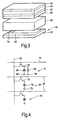
- Figure 3 shows a liquid crystal display, having an active plate 50 which comprises a substrate 51 over which there is provided an array 52 of pixel electrodes with associated switching transistors.
- the signals supplied to the pixel electrodes are controlled by row and driver circuits 54, also provided on the substrate.
- a layer of liquid crystal material 55 is provided over the active plate 50.
- a further substrate 56 overlies the layer of liquid crystal material. This further substrate 56 may be provided on one face with an arrangement of colour filters 57 and a plate defining a common electrode 64 for the liquid crystal material (explained further in connection with in Figure 4).
- a polarizing plate 58 is also provided on the opposite side of the substrate 56.
- Figure 4 shows the components located within the area of one pixel for a liquid crystal display device, when there are two memory cells within the vicinity of each pixel (as in Figure 2).
- Each pixel area comprises the pixel circuitry 16 and two memory cells 22.
- the pixel circuitry 16 comprises a thin film transistor 60 and a liquid crystal cell 62 arranged in series between the column conductor 20 and the common electrode 64.
- the transistor 60 is switched on and off by a signal provided on the row conductor 18.
- the row conductor 18 is thus connected to the gate of each transistor 60 of the associated row of pixels.
- Each pixel additionally comprises a storage capacitor 66, which in this example is connected to a separate capacitor electrode 68. It is instead possible for the storage capacitors to be connected to the previous row conductor, as will be apparent to those skilled in the art.
- the capacitor stores a drive voltage so that a signal is maintained across the liquid crystal cell 62 even after the transistor 60 has been turned off.
- an appropriate signal is provided on the column conductor 20 in synchronism with a row address pulse on the row conductor 18.
- This row address pulse turns on the thin film transistor 60, thereby allowing the column conductor 20 to charge the liquid crystal cell 62 to the desired voltage, and also to charge the storage capacitor 66 to the same voltage.
- the transistor 60 is turned off.
- the storage capacitor 66 maintains a voltage across the cell 62 and reduces the effect of liquid crystal leakage, as well as reducing the percentage variation in the pixel capacitance caused by the voltage dependency of the liquid crystal cell capacitance.
- Each memory cell 22 of the pixel area is associated with a different row conductor 28, but the column conductor 20 is shared. Each memory cell is thus associated with a unique combination of row and column address lines, and can therefore be addressed independently of the pixel circuitry 16.
- Each memory cell 22 comprises a thin film transistor 70 and a storage capacitor 72.
- the thin film transistors 70 are again switched on or off by the associated row conductors 28, thereby enabling a signal on the column conductor 20 to charge (or discharge) the storage capacitor 72.
- the storage capacitors of each memory cell are connected to a common electrode 73, which may be the same electrode as the common electrode 64 of the pixel circuits.
- the memory cells are fabricated from similar components to the components of the pixel circuitry 16. This enables layers within the structure to be shared between the different circuits, so that the introduction of the memory cells introduces minimum additional complexity to the manufacturing process. In particular, the same process steps are used to form the pixel circuits and the memory cells. It is possible to introduce no additional processing steps, although in some circumstances it may be necessary to introduce additional steps into the process. For example, an extra level of metallization may be added in order to simplify the layout of the memory cell circuits.
- the invention has particular benefit for reflective displays.
- the presence of additional circuits in the vicinity of the pixels does not affect the optical characteristics of the display, as they will lie beneath the reflective pixel electrode.
- Figure 5 shows schematically one possible arrangement of layers used to form the circuit shown in Figure 4.
- the structure is deposited on a common substrate, which may be provided with a planarization layer over the top surface.
- a patterned semiconductor (polycrystalline silicon) layer is deposited over the substrate defining the regions 80 shown in Figure 5.
- the semiconductor layer 80 is then processed using an additional doping step in order to implant dopant into areas of the polysilicon excluding those polysilicon areas which will form the semiconductor transistor 60,70 channels. This provides n-doped semiconductor regions, which have sufficient conductivity to be used to form electrodes within the circuits.
- a gate dielectric layer overlies the patterned and partially doped semiconductor layer, and the row electrodes 18, 28 as well as the capacitor top plates 68, 73 are deposited as a common metallization layer over the gate dielectric.
- the transistors 60, 70 are defined at the points where the row conductors 18, 28 cross over the undoped semiconductor patterns. In this way, top gate transistor structures are defined (with undoped channels). The higher conductivity doped semiconductor areas form the lower capacitor electrodes.
- the pixel capacitor 66 is therefore defined by the gate dielectric layer between the common electrode 68, defining one capacitor electrode, and the doped semiconductor layer 80, which defines the opposite electrode of the capacitor.
- Each memory cell capacitor 72 is defined by the gate dielectric layer between the common electrode 73 and the doped semiconductor layer 80 of the transistors 70 of the memory cells 22.
- a multiple-layer dielectric may be used, so that different dielectric thicknesses can be defined for the gate dielectric layer and for the capacitor dielectric layers.
- the column conductors 20 overlie this structure, and make contact to the source or drain of each transistor through vias 82.
- the pixel electrodes 61 overly this structure (over a planarising insulator) and make contact with the transistor 60 through via 84.
- the arrangement shown in Figure 5 thus provides the circuit layout of Figure 4.
- a DC voltage may be applied to the pixel top metal electrodes which is sufficient to invert the underlying silicon, thereby making the underlying silicon conducting.
- the memory structure may be used as a simple frame store for holding the video information to be shown on the display.
- the memory cells in the circuits of the invention can be used for functions other than holding the video information associated with any particular display pixel.
- the memory cells can be used to increase the functionality of the display in various ways.
- the memory may also be used to store information unrelated to the pixel information, for example pages of information such as ASCII characters which can be viewed on the display as additional information.
- the memory arrangement may be used for storing information completely unrelated to the information to be displayed, for example information concerning operation of the display, or even relating to other parts of the apparatus incorporating the display.
- memory cells There are many techniques which can be used for forming the memory cells. Essentially, conventional techniques used for forming MOS memories can be applied, although thin film transistors will be used in place of conventional crystalline silicon transistors.
- the memory cells may even be formed using ferroelectric or other materials which can be switched in a controlled way between two stable states.
- the use of some types of memory elements may require additional electrodes to be used to operate the memory circuits, for example a power source in the case of static RAM type memory cells.
- the memory cells may provide a read and write function, similar to conventional SRAM, DRAM or EEPROM memories, but the memory may also operate as a read only memory (ROM) to provide permanent storage of data within the display.
- ROM read only memory
- each pixel circuit is associated with two or four memory cells. There may in practice be many more memory cells associated with each pixel, depending on the amount of space available within each pixel area.
- the specific example shows layers shared between the pixel circuits and the memory cell circuits, so that the pixels and cells are effectively on the same plane over the substrate. It is possible to provide the pixel circuits and the memory cell circuits on different levels over the substrate. Although this will increase the manufacturing complexity, this is considered to lie within the scope of the invention.
Claims (9)
- Elektronische Anordnung, welche die nachfolgenden Elemente umfasst:eine Reihe von Pixeln (12), vorgesehen auf einem Substrat und gegliedert in Reihen und Spalten und mit einer Pixeltreiberschaltung (16),eine Anzahl Pixelreihe- und -spaltenadressleitungen zum Adressieren jedes Pixels (18, 20), wodurch Signaldaten an jedes Pixel oder Lesesignaldaten von jedem Pixel geliefert werden, undeine Reihe von Speicherzellen (22), vorgesehen auf dem Substrat und wobei die Pixeltreiberschaltung zwischengeschaltet ist, gekennzeichnet durch eine Speicheradressschaltung, vorgesehen zum Freigeben von Daten, die in jede Speicherzelle eingeschrieben werden müssen und zum Freigeben von Daten, die aus jeder Zelle ausgelesen werden müssen, und zwar unabhängig von den Signaldaten.
- Anordnung nach Anspruch 1, wobei die Speicheradressschaltung eine Anzahl Reihe- und Spaltespeicheradressleitungen (28, 30) hat zum Adressieren jeder Speicherzelle.
- Anordnung nach Anspruch 1, wobei die Speicheradressschaltung eine Anzahl Speicherreihenadressleitungen (28) aufweist und wobei jede Speicherzelle unter Verwendung einer assoziierten Speicherreihenadressleitung und einer der Pixelspaltenadressleitungen (30).
- Anordnung nach Anspruch 1, wobei die Speicheradressschaltung eine Anzahl Speicherspaltenadressleitungen (30) aufweist und wobei jede Speicherzelle unter Verwendung einer assoziierten Speicherspaltenadressleitung und einer der Pixelreihenadressleitungen (30) adressiert wird.
- Anordnung nach einem der vorstehenden Ansprüche, wobei jede Speicherzelle einen Transistor (70) und einen Kondensator (72) aufweist, wobei der Transistor es ermöglicht, dass der Kondensator aus einer gemeinsamen Speisung aufgeladen wird oder dass sonst der Kondensator gegenüber der gemeinsamen Speisung isoliert wird.
- Anordnung nach einem der vorstehenden Ansprüche, mit einer LCD-Anordnung, wobei jedes Pixel einen adressierenden Transistor (60) und einen Speicherkondensator (66) aufweist, wobei der adressierende Transistor es ermöglicht, dass der Kondensator aus einer gemeinsamen Speisung aufgeladen wird oder dass der Kondensator sonst gegenüber der gemeinsamen Speisung isoliert wird.
- Anordnung nach einem der vorstehenden Ansprüche, mit einer gleichen Anzahl Speicherzellen und Pixel.
- Anordnung nach einem der vorstehenden Ansprüche, mit einer Anzahl Speicherzellen, die ein ganzes Vielfaches ist, entsprechend oder größer als zwei der Anzahl Pixel.
- Anordnung nach einem der vorstehenden Ansprüche, wobei die Speicheradressschaltung eine Umwandlungsschaltung aufweist um ein Signaldatenformat in ein Speicherzellendatenformat umzuwandeln.
Applications Claiming Priority (3)
| Application Number | Priority Date | Filing Date | Title |
|---|---|---|---|
| GB0118183 | 2001-07-26 | ||
| GBGB0118183.3A GB0118183D0 (en) | 2001-07-26 | 2001-07-26 | Device comprising of an array of pixels |
| PCT/IB2002/002899 WO2003010746A1 (en) | 2001-07-26 | 2002-07-25 | Device comprising an array of pixels allowing storage of data |
Publications (2)
| Publication Number | Publication Date |
|---|---|
| EP1417672A1 EP1417672A1 (de) | 2004-05-12 |
| EP1417672B1 true EP1417672B1 (de) | 2005-08-17 |
Family
ID=9919197
Family Applications (1)
| Application Number | Title | Priority Date | Filing Date |
|---|---|---|---|
| EP02751471A Expired - Lifetime EP1417672B1 (de) | 2001-07-26 | 2002-07-25 | Anzeigevorrichtung mit einer pixel-matrix, die die speicherung von daten erlaubt |
Country Status (10)
| Country | Link |
|---|---|
| US (1) | US6937248B2 (de) |
| EP (1) | EP1417672B1 (de) |
| JP (1) | JP4644758B2 (de) |
| KR (1) | KR20040028621A (de) |
| CN (1) | CN1320517C (de) |
| AT (1) | ATE302460T1 (de) |
| DE (1) | DE60205636T2 (de) |
| GB (1) | GB0118183D0 (de) |
| TW (1) | TWI277039B (de) |
| WO (1) | WO2003010746A1 (de) |
Cited By (1)
| Publication number | Priority date | Publication date | Assignee | Title |
|---|---|---|---|---|
| CN101860688A (zh) * | 2009-04-08 | 2010-10-13 | 索尼公司 | 固态摄像器件和相机系统 |
Families Citing this family (10)
| Publication number | Priority date | Publication date | Assignee | Title |
|---|---|---|---|---|
| GB0206093D0 (en) * | 2002-03-15 | 2002-04-24 | Koninkl Philips Electronics Nv | Display driver and driving method |
| GB0213420D0 (en) * | 2002-06-12 | 2002-07-24 | Koninkl Philips Electronics Nv | In-Pixel memory for display devices |
| US7112815B2 (en) * | 2004-02-25 | 2006-09-26 | Micron Technology, Inc. | Multi-layer memory arrays |
| US20080001934A1 (en) * | 2006-06-28 | 2008-01-03 | David Anthony Wyatt | Apparatus and method for self-refresh in a display device |
| TW200841310A (en) * | 2007-04-10 | 2008-10-16 | Univ Nat Chiao Tung | Pixel driving circuit, and its driving method and application |
| JP2009210844A (ja) * | 2008-03-05 | 2009-09-17 | Toppoly Optoelectronics Corp | 液晶表示装置 |
| JP5264348B2 (ja) * | 2008-07-29 | 2013-08-14 | キヤノン株式会社 | 画像処理装置及びその制御方法、コンピュータプログラム及び記憶媒体 |
| KR101870892B1 (ko) | 2012-01-18 | 2018-06-26 | 삼성전자 주식회사 | 터치 스크린 장치 |
| US9734775B2 (en) * | 2014-02-13 | 2017-08-15 | Lenovo (Singapore) Pte. Ltd. | Display power saving utilizing non volatile memory |
| CN108961147B (zh) * | 2018-06-11 | 2022-12-13 | 北京集创北方科技股份有限公司 | 一种数据处理方法和装置 |
Family Cites Families (18)
| Publication number | Priority date | Publication date | Assignee | Title |
|---|---|---|---|---|
| US4688896A (en) * | 1985-03-04 | 1987-08-25 | General Electric Company | Information conversion device with auxiliary address lines for enhancing manufacturing yield |
| JPS6247696A (ja) * | 1985-08-28 | 1987-03-02 | 株式会社日立製作所 | 液晶表示装置 |
| JPH07120143B2 (ja) * | 1986-06-04 | 1995-12-20 | キヤノン株式会社 | 表示パネルの情報読出し法及び表示パネルの情報読出し装置 |
| JPH04291393A (ja) * | 1991-03-20 | 1992-10-15 | Fujitsu Ltd | 液晶表示装置及びその制御方法 |
| JP3102666B2 (ja) * | 1993-06-28 | 2000-10-23 | シャープ株式会社 | 画像表示装置 |
| US5945972A (en) * | 1995-11-30 | 1999-08-31 | Kabushiki Kaisha Toshiba | Display device |
| EP0797182A1 (de) * | 1996-03-19 | 1997-09-24 | Hitachi, Ltd. | Flüssigkristallanzeige mit aktiver Matrix und mit Datenhalteschaltung in jedem Pixel |
| US5952991A (en) | 1996-11-14 | 1999-09-14 | Kabushiki Kaisha Toshiba | Liquid crystal display |
| JP3533074B2 (ja) * | 1997-10-20 | 2004-05-31 | 日本電気株式会社 | Vram機能内蔵のledパネル |
| JP3832086B2 (ja) * | 1998-04-15 | 2006-10-11 | セイコーエプソン株式会社 | 反射型液晶装置及び反射型プロジェクタ |
| US6140983A (en) | 1998-05-15 | 2000-10-31 | Inviso, Inc. | Display system having multiple memory elements per pixel with improved layout design |
| WO2000014713A1 (en) * | 1998-09-04 | 2000-03-16 | Fed Corporation | Field sequential reflective liquid crystal display without external frame buffer |
| JP3788248B2 (ja) * | 2000-03-27 | 2006-06-21 | セイコーエプソン株式会社 | デジタル駆動装置およびこれを用いた画像表示装置 |
| JP2001296516A (ja) * | 2000-04-11 | 2001-10-26 | Seiko Epson Corp | 液晶表示装置、デジタルカメラおよびデジタルカメラ搭載複合機器 |
| JP2002056668A (ja) * | 2000-08-11 | 2002-02-22 | Thine Electronics Inc | 表示記憶機能付きマトリックス型画像表示装置の駆動回路装置 |
| JP2002189455A (ja) * | 2000-12-20 | 2002-07-05 | Seiko Epson Corp | 電気光学装置の駆動回路及び駆動方法 |
| US6817531B2 (en) * | 2001-03-07 | 2004-11-16 | Hewlett-Packard Development Company, L.P. | Apparatus and methods for marking content of memory storage devices |
| JP3530503B2 (ja) * | 2001-05-08 | 2004-05-24 | 三洋電機株式会社 | 表示装置 |
-
2001
- 2001-07-26 GB GBGB0118183.3A patent/GB0118183D0/en not_active Ceased
-
2002
- 2002-07-18 US US10/198,502 patent/US6937248B2/en not_active Expired - Lifetime
- 2002-07-25 TW TW091116570A patent/TWI277039B/zh not_active IP Right Cessation
- 2002-07-25 CN CNB028030281A patent/CN1320517C/zh not_active Expired - Lifetime
- 2002-07-25 KR KR10-2003-7004095A patent/KR20040028621A/ko not_active Application Discontinuation
- 2002-07-25 EP EP02751471A patent/EP1417672B1/de not_active Expired - Lifetime
- 2002-07-25 JP JP2003516043A patent/JP4644758B2/ja not_active Expired - Fee Related
- 2002-07-25 DE DE60205636T patent/DE60205636T2/de not_active Expired - Lifetime
- 2002-07-25 WO PCT/IB2002/002899 patent/WO2003010746A1/en active IP Right Grant
- 2002-07-25 AT AT02751471T patent/ATE302460T1/de not_active IP Right Cessation
Cited By (2)
| Publication number | Priority date | Publication date | Assignee | Title |
|---|---|---|---|---|
| CN101860688A (zh) * | 2009-04-08 | 2010-10-13 | 索尼公司 | 固态摄像器件和相机系统 |
| CN101860688B (zh) * | 2009-04-08 | 2012-10-31 | 索尼公司 | 固态摄像器件和相机系统 |
Also Published As
| Publication number | Publication date |
|---|---|
| ATE302460T1 (de) | 2005-09-15 |
| DE60205636T2 (de) | 2006-06-08 |
| JP2004538505A (ja) | 2004-12-24 |
| TWI277039B (en) | 2007-03-21 |
| KR20040028621A (ko) | 2004-04-03 |
| DE60205636D1 (de) | 2005-09-22 |
| JP4644758B2 (ja) | 2011-03-02 |
| US6937248B2 (en) | 2005-08-30 |
| EP1417672A1 (de) | 2004-05-12 |
| CN1476596A (zh) | 2004-02-18 |
| WO2003010746A1 (en) | 2003-02-06 |
| US20030020684A1 (en) | 2003-01-30 |
| CN1320517C (zh) | 2007-06-06 |
| GB0118183D0 (en) | 2001-09-19 |
Similar Documents
| Publication | Publication Date | Title |
|---|---|---|
| US8144102B2 (en) | Memory element and display device | |
| US7542024B2 (en) | Electrophoresis display device and electronic equipments using the same | |
| US6771247B2 (en) | Display and method of driving display | |
| EP1362339B1 (de) | Organische leuchtdioden-pixel-schaltung mit geringer stromaufnahme | |
| JP2002229532A (ja) | 液晶表示装置及び液晶表示装置の駆動方法 | |
| EP1417672B1 (de) | Anzeigevorrichtung mit einer pixel-matrix, die die speicherung von daten erlaubt | |
| EP1516307B1 (de) | Mram speicher für bildelemente von anzeigevorrichtungen | |
| KR100406454B1 (ko) | 표시 장치 및 그 구동 방법 | |
| KR101073364B1 (ko) | 디스플레이 디바이스 | |
| US7257007B2 (en) | Spacers for cells having spaced opposed substrates | |
| KR100472269B1 (ko) | 액티브 매트릭스형 표시 장치 | |
| US20020060674A1 (en) | Active matrix display device | |
| US20060181495A1 (en) | Active matrix array device | |
| US20080094380A1 (en) | Electronic Device With Multiple Array Devices | |
| US7245296B2 (en) | Active matrix display device | |
| CN114863885A (zh) | 一种像素电路、阵列基板及显示装置 | |
| JPH08146384A (ja) | アクティブマトリックス型液晶表示素子 |
Legal Events
| Date | Code | Title | Description |
|---|---|---|---|
| PUAI | Public reference made under article 153(3) epc to a published international application that has entered the european phase |
Free format text: ORIGINAL CODE: 0009012 |
|
| 17P | Request for examination filed |
Effective date: 20040226 |
|
| AK | Designated contracting states |
Kind code of ref document: A1 Designated state(s): AT BE BG CH CY CZ DE DK EE ES FI FR GB GR IE IT LI LU MC NL PT SE SK TR |
|
| GRAP | Despatch of communication of intention to grant a patent |
Free format text: ORIGINAL CODE: EPIDOSNIGR1 |
|
| RIC1 | Information provided on ipc code assigned before grant |
Ipc: 7G 09G 3/20 B Ipc: 7G 11C 8/14 B Ipc: 7G 09G 3/36 A |
|
| RIC1 | Information provided on ipc code assigned before grant |
Ipc: 7G 09G 3/20 B Ipc: 7G 11C 8/14 B Ipc: 7G 09G 3/36 A |
|
| GRAS | Grant fee paid |
Free format text: ORIGINAL CODE: EPIDOSNIGR3 |
|
| GRAA | (expected) grant |
Free format text: ORIGINAL CODE: 0009210 |
|
| AK | Designated contracting states |
Kind code of ref document: B1 Designated state(s): AT BE BG CH CY CZ DE DK EE ES FI FR GB GR IE IT LI LU MC NL PT SE SK TR |
|
| PG25 | Lapsed in a contracting state [announced via postgrant information from national office to epo] |
Ref country code: IT Free format text: LAPSE BECAUSE OF FAILURE TO SUBMIT A TRANSLATION OF THE DESCRIPTION OR TO PAY THE FEE WITHIN THE PRESCRIBED TIME-LIMIT;WARNING: LAPSES OF ITALIAN PATENTS WITH EFFECTIVE DATE BEFORE 2007 MAY HAVE OCCURRED AT ANY TIME BEFORE 2007. THE CORRECT EFFECTIVE DATE MAY BE DIFFERENT FROM THE ONE RECORDED. Effective date: 20050817 Ref country code: BE Free format text: LAPSE BECAUSE OF FAILURE TO SUBMIT A TRANSLATION OF THE DESCRIPTION OR TO PAY THE FEE WITHIN THE PRESCRIBED TIME-LIMIT Effective date: 20050817 Ref country code: TR Free format text: LAPSE BECAUSE OF FAILURE TO SUBMIT A TRANSLATION OF THE DESCRIPTION OR TO PAY THE FEE WITHIN THE PRESCRIBED TIME-LIMIT Effective date: 20050817 Ref country code: LI Free format text: LAPSE BECAUSE OF FAILURE TO SUBMIT A TRANSLATION OF THE DESCRIPTION OR TO PAY THE FEE WITHIN THE PRESCRIBED TIME-LIMIT Effective date: 20050817 Ref country code: NL Free format text: LAPSE BECAUSE OF FAILURE TO SUBMIT A TRANSLATION OF THE DESCRIPTION OR TO PAY THE FEE WITHIN THE PRESCRIBED TIME-LIMIT Effective date: 20050817 Ref country code: AT Free format text: LAPSE BECAUSE OF FAILURE TO SUBMIT A TRANSLATION OF THE DESCRIPTION OR TO PAY THE FEE WITHIN THE PRESCRIBED TIME-LIMIT Effective date: 20050817 Ref country code: SK Free format text: LAPSE BECAUSE OF FAILURE TO SUBMIT A TRANSLATION OF THE DESCRIPTION OR TO PAY THE FEE WITHIN THE PRESCRIBED TIME-LIMIT Effective date: 20050817 Ref country code: CZ Free format text: LAPSE BECAUSE OF FAILURE TO SUBMIT A TRANSLATION OF THE DESCRIPTION OR TO PAY THE FEE WITHIN THE PRESCRIBED TIME-LIMIT Effective date: 20050817 Ref country code: EE Free format text: LAPSE BECAUSE OF FAILURE TO SUBMIT A TRANSLATION OF THE DESCRIPTION OR TO PAY THE FEE WITHIN THE PRESCRIBED TIME-LIMIT Effective date: 20050817 Ref country code: CH Free format text: LAPSE BECAUSE OF FAILURE TO SUBMIT A TRANSLATION OF THE DESCRIPTION OR TO PAY THE FEE WITHIN THE PRESCRIBED TIME-LIMIT Effective date: 20050817 Ref country code: FI Free format text: LAPSE BECAUSE OF FAILURE TO SUBMIT A TRANSLATION OF THE DESCRIPTION OR TO PAY THE FEE WITHIN THE PRESCRIBED TIME-LIMIT Effective date: 20050817 |
|
| REG | Reference to a national code |
Ref country code: GB Ref legal event code: FG4D |
|
| REG | Reference to a national code |
Ref country code: CH Ref legal event code: EP |
|
| REG | Reference to a national code |
Ref country code: IE Ref legal event code: FG4D |
|
| REF | Corresponds to: |
Ref document number: 60205636 Country of ref document: DE Date of ref document: 20050922 Kind code of ref document: P |
|
| PG25 | Lapsed in a contracting state [announced via postgrant information from national office to epo] |
Ref country code: DK Free format text: LAPSE BECAUSE OF FAILURE TO SUBMIT A TRANSLATION OF THE DESCRIPTION OR TO PAY THE FEE WITHIN THE PRESCRIBED TIME-LIMIT Effective date: 20051117 Ref country code: GR Free format text: LAPSE BECAUSE OF FAILURE TO SUBMIT A TRANSLATION OF THE DESCRIPTION OR TO PAY THE FEE WITHIN THE PRESCRIBED TIME-LIMIT Effective date: 20051117 Ref country code: SE Free format text: LAPSE BECAUSE OF FAILURE TO SUBMIT A TRANSLATION OF THE DESCRIPTION OR TO PAY THE FEE WITHIN THE PRESCRIBED TIME-LIMIT Effective date: 20051117 Ref country code: BG Free format text: LAPSE BECAUSE OF FAILURE TO SUBMIT A TRANSLATION OF THE DESCRIPTION OR TO PAY THE FEE WITHIN THE PRESCRIBED TIME-LIMIT Effective date: 20051117 |
|
| PG25 | Lapsed in a contracting state [announced via postgrant information from national office to epo] |
Ref country code: ES Free format text: LAPSE BECAUSE OF FAILURE TO SUBMIT A TRANSLATION OF THE DESCRIPTION OR TO PAY THE FEE WITHIN THE PRESCRIBED TIME-LIMIT Effective date: 20051128 |
|
| PG25 | Lapsed in a contracting state [announced via postgrant information from national office to epo] |
Ref country code: PT Free format text: LAPSE BECAUSE OF FAILURE TO SUBMIT A TRANSLATION OF THE DESCRIPTION OR TO PAY THE FEE WITHIN THE PRESCRIBED TIME-LIMIT Effective date: 20060117 |
|
| NLV1 | Nl: lapsed or annulled due to failure to fulfill the requirements of art. 29p and 29m of the patents act | ||
| REG | Reference to a national code |
Ref country code: CH Ref legal event code: PL |
|
| ET | Fr: translation filed | ||
| PLBE | No opposition filed within time limit |
Free format text: ORIGINAL CODE: 0009261 |
|
| STAA | Information on the status of an ep patent application or granted ep patent |
Free format text: STATUS: NO OPPOSITION FILED WITHIN TIME LIMIT |
|
| PG25 | Lapsed in a contracting state [announced via postgrant information from national office to epo] |
Ref country code: IE Free format text: LAPSE BECAUSE OF NON-PAYMENT OF DUE FEES Effective date: 20060725 |
|
| 26N | No opposition filed |
Effective date: 20060518 |
|
| PG25 | Lapsed in a contracting state [announced via postgrant information from national office to epo] |
Ref country code: MC Free format text: LAPSE BECAUSE OF NON-PAYMENT OF DUE FEES Effective date: 20060731 |
|
| REG | Reference to a national code |
Ref country code: IE Ref legal event code: MM4A |
|
| PG25 | Lapsed in a contracting state [announced via postgrant information from national office to epo] |
Ref country code: LU Free format text: LAPSE BECAUSE OF NON-PAYMENT OF DUE FEES Effective date: 20060725 |
|
| PG25 | Lapsed in a contracting state [announced via postgrant information from national office to epo] |
Ref country code: CY Free format text: LAPSE BECAUSE OF FAILURE TO SUBMIT A TRANSLATION OF THE DESCRIPTION OR TO PAY THE FEE WITHIN THE PRESCRIBED TIME-LIMIT Effective date: 20050817 |
|
| REG | Reference to a national code |
Ref country code: GB Ref legal event code: 732E Free format text: REGISTERED BETWEEN 20090122 AND 20090128 |
|
| REG | Reference to a national code |
Ref country code: FR Ref legal event code: TP |
|
| REG | Reference to a national code |
Ref country code: DE Ref legal event code: R082 Ref document number: 60205636 Country of ref document: DE |
|
| REG | Reference to a national code |
Ref country code: FR Ref legal event code: PLFP Year of fee payment: 14 |
|
| REG | Reference to a national code |
Ref country code: FR Ref legal event code: PLFP Year of fee payment: 15 |
|
| REG | Reference to a national code |
Ref country code: FR Ref legal event code: PLFP Year of fee payment: 16 |
|
| REG | Reference to a national code |
Ref country code: FR Ref legal event code: PLFP Year of fee payment: 17 |
|
| PGFP | Annual fee paid to national office [announced via postgrant information from national office to epo] |
Ref country code: FR Payment date: 20180612 Year of fee payment: 17 |
|
| PGFP | Annual fee paid to national office [announced via postgrant information from national office to epo] |
Ref country code: DE Payment date: 20180710 Year of fee payment: 17 |
|
| PGFP | Annual fee paid to national office [announced via postgrant information from national office to epo] |
Ref country code: GB Payment date: 20180725 Year of fee payment: 17 |
|
| REG | Reference to a national code |
Ref country code: DE Ref legal event code: R119 Ref document number: 60205636 Country of ref document: DE |
|
| GBPC | Gb: european patent ceased through non-payment of renewal fee |
Effective date: 20190725 |
|
| PG25 | Lapsed in a contracting state [announced via postgrant information from national office to epo] |
Ref country code: GB Free format text: LAPSE BECAUSE OF NON-PAYMENT OF DUE FEES Effective date: 20190725 Ref country code: DE Free format text: LAPSE BECAUSE OF NON-PAYMENT OF DUE FEES Effective date: 20200201 |
|
| PG25 | Lapsed in a contracting state [announced via postgrant information from national office to epo] |
Ref country code: FR Free format text: LAPSE BECAUSE OF NON-PAYMENT OF DUE FEES Effective date: 20190731 |