EP1413905A1 - Optisches modul und herstellungsverfahren dafür - Google Patents
Optisches modul und herstellungsverfahren dafür Download PDFInfo
- Publication number
- EP1413905A1 EP1413905A1 EP02771740A EP02771740A EP1413905A1 EP 1413905 A1 EP1413905 A1 EP 1413905A1 EP 02771740 A EP02771740 A EP 02771740A EP 02771740 A EP02771740 A EP 02771740A EP 1413905 A1 EP1413905 A1 EP 1413905A1
- Authority
- EP
- European Patent Office
- Prior art keywords
- alignment
- recess
- optical
- sol
- recesses
- Prior art date
- Legal status (The legal status is an assumption and is not a legal conclusion. Google has not performed a legal analysis and makes no representation as to the accuracy of the status listed.)
- Withdrawn
Links
- 230000003287 optical effect Effects 0.000 title claims abstract description 95
- 238000004519 manufacturing process Methods 0.000 title description 3
- 239000000758 substrate Substances 0.000 claims abstract description 79
- 239000013307 optical fiber Substances 0.000 claims abstract description 64
- 239000000463 material Substances 0.000 claims abstract description 19
- 238000000034 method Methods 0.000 claims description 30
- 239000000853 adhesive Substances 0.000 claims description 27
- 230000001070 adhesive effect Effects 0.000 claims description 27
- 238000000016 photochemical curing Methods 0.000 claims description 18
- 229920005989 resin Polymers 0.000 claims description 13
- 239000011347 resin Substances 0.000 claims description 13
- 238000001723 curing Methods 0.000 claims description 8
- 238000003825 pressing Methods 0.000 claims description 8
- 230000001678 irradiating effect Effects 0.000 claims 2
- 238000003754 machining Methods 0.000 description 8
- 230000008569 process Effects 0.000 description 5
- 238000003848 UV Light-Curing Methods 0.000 description 3
- 238000003491 array Methods 0.000 description 3
- 230000003247 decreasing effect Effects 0.000 description 3
- 230000001105 regulatory effect Effects 0.000 description 3
- 230000004075 alteration Effects 0.000 description 2
- 230000008859 change Effects 0.000 description 2
- 230000000694 effects Effects 0.000 description 2
- 238000005530 etching Methods 0.000 description 2
- 238000001459 lithography Methods 0.000 description 2
- 238000000465 moulding Methods 0.000 description 2
- XUIMIQQOPSSXEZ-UHFFFAOYSA-N Silicon Chemical compound [Si] XUIMIQQOPSSXEZ-UHFFFAOYSA-N 0.000 description 1
- 230000005540 biological transmission Effects 0.000 description 1
- 230000015572 biosynthetic process Effects 0.000 description 1
- 238000004140 cleaning Methods 0.000 description 1
- 238000010276 construction Methods 0.000 description 1
- 238000005553 drilling Methods 0.000 description 1
- 239000003822 epoxy resin Substances 0.000 description 1
- 239000004973 liquid crystal related substance Substances 0.000 description 1
- 229920000647 polyepoxide Polymers 0.000 description 1
- 230000009467 reduction Effects 0.000 description 1
- 229910052710 silicon Inorganic materials 0.000 description 1
- 239000010703 silicon Substances 0.000 description 1
Images


Classifications
-
- G—PHYSICS
- G02—OPTICS
- G02B—OPTICAL ELEMENTS, SYSTEMS OR APPARATUS
- G02B6/00—Light guides; Structural details of arrangements comprising light guides and other optical elements, e.g. couplings
- G02B6/24—Coupling light guides
- G02B6/36—Mechanical coupling means
- G02B6/3628—Mechanical coupling means for mounting fibres to supporting carriers
- G02B6/3632—Mechanical coupling means for mounting fibres to supporting carriers characterised by the cross-sectional shape of the mechanical coupling means
- G02B6/3644—Mechanical coupling means for mounting fibres to supporting carriers characterised by the cross-sectional shape of the mechanical coupling means the coupling means being through-holes or wall apertures
-
- G—PHYSICS
- G02—OPTICS
- G02B—OPTICAL ELEMENTS, SYSTEMS OR APPARATUS
- G02B6/00—Light guides; Structural details of arrangements comprising light guides and other optical elements, e.g. couplings
- G02B6/24—Coupling light guides
- G02B6/26—Optical coupling means
- G02B6/32—Optical coupling means having lens focusing means positioned between opposed fibre ends
- G02B6/322—Optical coupling means having lens focusing means positioned between opposed fibre ends and having centering means being part of the lens for the self-positioning of the lightguide at the focal point, e.g. holes, wells, indents, nibs
-
- G—PHYSICS
- G02—OPTICS
- G02B—OPTICAL ELEMENTS, SYSTEMS OR APPARATUS
- G02B6/00—Light guides; Structural details of arrangements comprising light guides and other optical elements, e.g. couplings
- G02B6/24—Coupling light guides
- G02B6/36—Mechanical coupling means
- G02B6/3628—Mechanical coupling means for mounting fibres to supporting carriers
- G02B6/3664—2D cross sectional arrangements of the fibres
- G02B6/3672—2D cross sectional arrangements of the fibres with fibres arranged in a regular matrix array
-
- G—PHYSICS
- G02—OPTICS
- G02B—OPTICAL ELEMENTS, SYSTEMS OR APPARATUS
- G02B6/00—Light guides; Structural details of arrangements comprising light guides and other optical elements, e.g. couplings
- G02B6/24—Coupling light guides
- G02B6/36—Mechanical coupling means
- G02B6/3628—Mechanical coupling means for mounting fibres to supporting carriers
- G02B6/3684—Mechanical coupling means for mounting fibres to supporting carriers characterised by the manufacturing process of surface profiling of the supporting carrier
- G02B6/3696—Mechanical coupling means for mounting fibres to supporting carriers characterised by the manufacturing process of surface profiling of the supporting carrier by moulding, e.g. injection moulding, casting, embossing, stamping, stenciling, printing, or with metallic mould insert manufacturing using LIGA or MIGA techniques
Definitions
- the present invention generally relates to an optical module, particularly to an optical module which is densely space-division multiplexed by using a microlens array, and a method for fabricating the optical module.
- a conventional optical module of this type has been disclosed in Japanese patent No.2719804, for example.
- This conventional optical module comprises, as shown in Fig.1, a planar microlens array 60 consisting of a planar transparent substrate having circular microlenses 61 formed in a surface thereof. Fitting recesses 65 are formed in a surface opposite to the lens-formed surface of the array 60, each of recesses 65 being aligned with the center of a corresponding microlens 61.
- An optical element to be optically coupled to the microlens 61 is an optical fiber 63, for example. The end core portion of an optical fiber is processed by a selective etching to form a micro fitting convex portion 66.
- an alignment can easily be conducted by inserting the convex portion 66 of an optical fiber into the fitting recess 65 to fix it thereto, instead of an active alignment (i.e., light is guided into an optical fiber and the position of the optical fiber is regulated so as to maximize light coupled to a microlens).
- an active alignment i.e., light is guided into an optical fiber and the position of the optical fiber is regulated so as to maximize light coupled to a microlens.
- the light from the end of the optical fiber 63 is transferred into collimated light 100 by means of the microlens 61.
- a machining such as a laser beam machining, a drilling, or an ultrasonic machining is used as a method for opening holes.
- a laser beam machining is a relatively low cost method, it has problems such that the control of a diameter of a hole is difficult resulting in a low circular degree of a hole, and furthermore the taper of a guide hole is not preferably controlled.
- the kind of a material for a substrate to be processed is limited.
- a backing to a substrate is required to prevent a chipping (i.e., a partial peeling of a substrate) from being caused on a bottom side of a substrate.
- a chipping may not be completely prevented for a backed substrate.
- An adhering, separating and cleaning steps are further required for backing a substrate.
- an aligning process between a planar microlens array and a guide substrate for optical fibers is required during the assembling of an optical module.
- the coefficient of thermal expansion of a microlens array substrate and that of a guide substrate for optical fibers must be the same.
- an object of the present invention is to provide an optical module wherein recesses are formed in a sol-gel layer applied to a surface of a lens array substrate, each of the recesses having a capability to fit an optical fiber therein.
- Another object of the present invention is to provide an optical module in which an inlet portion of a recess formed in the sol-gel layer has a capability to guide an optical fiber therein.
- a further object of the present invention is to provide an optical module in which an optical element is formed at a bottom portion of the recess formed in the sol-gel layer.
- a still further object of the present invention is to provide a method for fabricating the optical module described above.
- a first aspect of the present invention is an optical module comprising a planar microlens array substrate having a plurality of microlenses formed in one surface thereof ; and an alignment recess array including a plurality of alignment recesses which are formed in a material applied to the other surface of the microlens array substrate by means of a mold with the center of each alignment recess being aligned to the center of a corresponding one of the microlens.
- a second aspect of the present invention is an optical module comprising a planar microlens array substrate having a plurality of microlenses formed in at least one surface thereof ; a planar transparent substrate for adjusting a conjugate ratio, one surface thereof being adhered to a surface of the lens array substrate; and an alignment recess array including a plurality of alignment recesses which are formed in a material applied to the other surface of the transparent substrate by means of a mold with the center of each alignment recess being aligned to the center of a corresponding one of the microlens.
- an inlet portion of each alignment recess has a tapered portion for guiding an optical fiber to be inserted into the alignment recess.
- an optical element formed at the bottom of an alignment recess.
- optical modules comprise a plurality of optical fibers each end thereof is adhered to the alignment recesses.
- a third aspect of the present invention is a method for fabricating an optical module comprising the steps of preparing a mold having convex portions to form a plurality of alignment recesses for optical fibers ; providing a sol-gel layer by applying a sol-gel material on one surface of a planar microlens array substrate having a plurality of microlenses formed in the other surface thereof ; forming the alignment recesses by pressing the mold to the sol-gel layer to transfer the convex portions to the sol-gel layer ; and baking and curing the sol-gel layer in which the alignment recesses are formed.
- a fourth aspect of the present invention is a method for fabricating an optical module comprising the steps of preparing a mold having convex portions to form a plurality of alignment recesses for optical fibers ; providing a sol-gel layer by applying a sol-gel material on one surface of a planar transparent substrate for adjusting a conjugate ratio, forming the alignment recesses by pressing the mold to the sol-gel layer to transfer the convex portions to the sol-gel layer ; baking and curing the sol-gel layer in which the alignment recesses are formed ; and adhering the other surface of the transparent substrate to one surface of a planar microlens array substrate having a plurality of microlenses formed in the other surface thereof with the center of each alignment recesses being aligned the center of a corresponding one of the microlens.
- the step of forming the alignment recesses includes forming a tapered portion at an inlet portion of each alignment recess for guiding an optical fiber to be inserted into the alignment recess.
- the step of forming the alignment recesses includes forming a recess for an optical element at the bottom of the alignment recess.
- These methods further comprise the steps of fitting the end of an optical fiber to the alignment recess; and adhering the end of an optical fiber to the alignment recess by adhesive.
- FIG.2 there is shown a first embodiment of an optical module according to the present invention.
- an alignment recess array consisting of a sol-gel layer 16 is fabricated on a surface (i.e., a surface to which optical fibers are connected) of the lens array substrate 12.
- reference numeral 18 denotes an alignment recess.
- the recess array is fabricated by applying a sol-gel material to a surface of the lens array and by pressing a mold to the sol-gel material form recesses.
- Figs.3A and 3B show a plan view and side view of a mold 20 to be used.
- the mold is fabricated by a machining, which comprises 4 ⁇ 4 cylindrical convex portion 22 arranged in a 250 ⁇ m pitch, each thereof having a diameter of 127 ⁇ m and a height of 30 ⁇ m.
- a sol-gel material 24 is applied to a surface of the lens array 12 to which optical fiber are connected to form a sol-gel layer of approximately 35 ⁇ m thick.
- the mold 20 is pressed to the sol-gel layer with the position of the lenses and that of the convex portions of the mold being aligned thereby transferring the shape of the convex portion to the sol-gel layer.
- the mold 20 is released as shown in Fig.4C.
- the lens array substrate 12 provided with a formed sol-gel layer is baked to cure the sol-gel layer.
- the thickness of the baked sol-gel layer 16 may be in a range of 30 ⁇ 3 ⁇ m, the diameter of the cylindrical recess may be in a range of 127 ⁇ 2 ⁇ m, and the pitch of recesses may be in a range of 250 ⁇ 2 ⁇ m.
- a misalignment of an optical fiber with respect to an optical axis of the microlens may be in a range of ⁇ 2 ⁇ m.
- a UV-curing adhesive is applied in the recesses 18 formed in the sol-gel layer 16, the ends of the optical fibers are fitted to the recesses, and UV ray is irradiated to adhere the ends of the optical fibers to the recesses.
- a thin sol-gel layer is left on the bottom of the recess 18 formed by a press molding.
- the thickness of the thin sol-gel layer is less than 1 ⁇ m which is the level not effecting an optical property.
- the thickness of the baked sol-gel layer (30 ⁇ 3 ⁇ m) is fully thin in comparison with the thickness of 3mm of the lens array substrate 12, so that it is understood that a stress due to a temperature change is not caused therein.
- a resin such as epoxy resin, photo (ultraviolet)-curing resin and the like may be used.
- the photo-curing resin is applied to the surface of the lens array substrate to which optical fibers are connected, and then a mold is pressed against the resin. Ultraviolet ray is irradiated to cure the resin. The mold is released and then a baking is implemented.
- the shape of the alignment recess 18 is a cylinder the diameter thereof is 127 ⁇ m, a prism such as a triangle pole, a square pole and the like to which a circle of 127 ⁇ m diameter is inscribed.
- a mold having prismatic convex portions is required. The prismatic convex portions are easily made rather than the cylindrical convex portions in view of machining for a mold.
- an alignment recess is not limited to a column such as a cylinder or prism as described above, but the inlet portion of an alignment recess may be tapered.
- FIG.5A shows a total view of an optical module
- Fig.5B an enlarged view of an alignment recess 26.
- the recess 26 consists of an inlet portion consisting of circular cone (taper angle is 30° ) the depth thereof is 20 ⁇ m and a bottom portion consisting of a cylinder the depth thereof is 20 ⁇ m.
- a mold is fabricated by a machining, it may be fabricated by etching a silicon substrate using a lithography process.
- a guide substrate for optical fibers may be separately provided, in which tapered guide holes are opened.
- a lens-shape portion is formed on the top of a column portion of a mold.
- the lens-shape portion is transferred to a sol-gel layer together with an alignment recess.
- Figs.6A and 6B show a plan view and side view of a mold 30 used in the present embodiment.
- a mold 30 is formed having a semi-spherical portion 34 (the radius of curvature R of the part is 30 ⁇ m) on the top of the cylindrical convex portion 32 (the diameter thereof is 127 ⁇ m).
- alignment recesses are formed in the sol-gel layer 16 applied on the surface of the lens array substrate 12, in the same manner as in the embodiment 1.
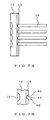
- Fig.7A shows a total view of an optical module of the present embodiment
- Fig.7B an enlarged view of a recess 40 transferred in the sol-gel layer 16.
- the cylindrical convex portion 32 of the mold 30 is transferred to form an alignment recess 42 in the inlet portion of the recess 40
- the semi-spherical portion 34 on the top of the cylindrical convex portion is transferred to form a recess 44 for a lens at the bottom of the alignment recess 42.
- An optical fiber 14 is adhered to the recess 40 in the sol-gel layer 16 by using UV-curing adhesive which has an index of refraction larger than that of the sol-gel material, with the recess 44 for a lens being filled with the adhesive.
- Fig.8 there is shown an enlarged view of the recess to which an optical fiber is adhered.
- the adhesive 50 is filled in the recess 44 for a lens.
- an index of refraction of the lens array substrate 12 is 1.54
- that of the sol-gel layer 16 is 1.3
- that of the UV-curing adhesive 50 is approximately 1.6
- the recess 44 may serve as a spherical lens.
- the optical module of the present embodiment functions a two-lens optical system, so that the numerical aperture (NA) the optical module is smaller in comparison with that of the optical module in the first embodiment thereby decreasing the aberration thereof.
- NA numerical aperture
- an aspherical lens may be formed.
- An optical prism, beam splitter, or diffraction grating may also be formed at the bottom of the recess.
- the optical module according to the first or second embodiments has a structure such that the optical fibers are directly connected to the lens array substrate.
- a planar optical element e.g., a planar transmission optical element module such as a liquid crystal optical switch
- a microlens optical system of the optical module must be constructed by a collimate optical system having an infinite conjugate ratio.
- the optical module is coupled to a light-emitting element such as a layer array
- a microlens system of the optical module must be constructed by a reduction image optical system having a finite conjugate ratio.
- the conjugate ratio means the ratio of an object distance to an image distance.
- a microlens optical system In the case of an optical module coupled to optical fibers, a microlens optical system is required to be constructed by a unity magnification image optical system, while in the case of an optical module coupled to a planar optical element such as a photo-detector array having a light-receiving area larger than a mode field diameter of an optical fiber, a microlens optical system is required to be constructed by a magnification image optical system.
- planar microlens arrays each having a different focal length of microlens are prepared separately so that an optimal conjugate ratio may be obtained for respective application in the conventional optical module, or the thickness of a planar microlens array substrate is regulated to obtain an optimal conjugate ratio.
- the number of kinds of planar microlens arrays will be increased.
- the optical characteristic of an optical module is regulated in an experimental environment for example, it is often required to remake a planar microlens array. In such a case, an efficient development and early implementation of optical modules will be disturbed.
- a transparent substrate for adjusting a conjugate ratio may be provided between a planar lens array substrate and optical fibers.
- FIGs.9A and 9B there is shown an embodiment of an optical module using a transparent substrate for adjusting a conjugate ratio.
- the optical module comprises a transparent substrate 60 for adjusting a conjugate ratio provided between a lens array substrate 12 and a sol-gel layer 16. An infinite conjugate ratio may be obtained by the transparent substrate 60.
- the light from the end of the optical fiber 14 is transferred into the collimated light 100 by means of the microlenses 10.
- the difference between the optical modules in Figs.9A and 9B is that the positions where the microlenses 10 are formed in the lens array 12 are different. That is, the microlenses 10 are formed in one surface to which the transparent substrate 60 is faced in Fig.9A, and the microlenses 10 are formed in the other surface in Fig.9B.
- a sol-gel material is applied to one surface of the transparent substrate 60 to form a sol-gel layer 16
- a mold is pressed to the sol-gel layer to form alignment recesses 26, and the formed sol-gel layer is baked and cured.
- the other surface of the transparent substrate 60 is adhered to the surface of the lens array 12 with the center of the alignment recess 26 is matched to the center of the microlens 10.
- optical fibers are inserted into the alignment recesses 26 and adhered thereto by adhesive.
- the reason why at first the sol-gel layer is applied to the transparent substrate 60 to form the alignment recesses 26, and subsequently the transparent substrate 60 is adhered to the lens substrate 12 is as follows.
- the baking and curing of the sol-gel layer is implemented at a high temperature of 300-500°C. Therefore, if at first the transparent substrate is adhered to the lens substrate 12 by adhesive, and subsequently the sol-gel layer is applied, the adhesive can not bear with such a high temperature.
- a lens array substrate may be replaced by a planar microlens array on both surfaces thereof microlenses are formed.
- a plurality of planar microlens arrays stacked and adhered to each other may also be used as a lens array substrate.
- an optical element may be formed at the bottom of an alignment recess in a sol-gel layer as illustrated in the second embodiment.
- a photo-curing resin may also be used in place of a sol-gel material.
- a baking is not required for a photo-curing resin, so that at first a lens array substrate 12 and a transparent substrate 60 may be adhered, and subsequently a photo-curing resin may be applied to the transparent substrate 60 to form alignment recesses.
- a photo-curing resin may be applied to the transparent substrate 60 to form alignment recesses, and subsequently a lens array substrate 12 may be adhered to the transparent substrate 60 with aligning the centers of a microlens and an alignment recess.
- a recess array for aligning optical fibers to a lens array substrate may be fabricated by a forming process at a high precision and low cost.
- a tapered portion for guiding an optical fiber may also be fabricated by designing the shape of a mold.
- optical element such as lenses, beam splitters, diffraction gratings or the like may be formed together with an alignment recess array, the optical elements serving as spectroscopic elements, collective elements or the like. If lenses are formed at the bottoms of alignment recesses, a two-lens optical system is structured together with a microlens of a lens array substrate, so that there are effects such as decreased numerical aperture (NA) or decreased aberration.
- NA numerical aperture
Landscapes
- Physics & Mathematics (AREA)
- General Physics & Mathematics (AREA)
- Optics & Photonics (AREA)
- Optical Couplings Of Light Guides (AREA)
Applications Claiming Priority (3)
| Application Number | Priority Date | Filing Date | Title |
|---|---|---|---|
| JP2001153541A JP2002350674A (ja) | 2001-05-23 | 2001-05-23 | 光モジュールおよびその製造方法 |
| JP2001153541 | 2001-05-23 | ||
| PCT/JP2002/004878 WO2002095465A1 (fr) | 2001-05-23 | 2002-05-21 | Module optique et procede de production associe |
Publications (2)
| Publication Number | Publication Date |
|---|---|
| EP1413905A1 true EP1413905A1 (de) | 2004-04-28 |
| EP1413905A4 EP1413905A4 (de) | 2005-05-11 |
Family
ID=18998042
Family Applications (1)
| Application Number | Title | Priority Date | Filing Date |
|---|---|---|---|
| EP02771740A Withdrawn EP1413905A4 (de) | 2001-05-23 | 2002-05-21 | Optisches modul und herstellungsverfahren dafür |
Country Status (5)
| Country | Link |
|---|---|
| US (1) | US7236665B2 (de) |
| EP (1) | EP1413905A4 (de) |
| JP (1) | JP2002350674A (de) |
| CA (1) | CA2448199A1 (de) |
| WO (1) | WO2002095465A1 (de) |
Cited By (5)
| Publication number | Priority date | Publication date | Assignee | Title |
|---|---|---|---|---|
| EP1722257A1 (de) * | 2005-05-10 | 2006-11-15 | Blz Bayerisches Laserzentrum Gemeinnützige Forschungsges. Mbh | Linsenarray |
| WO2008116808A1 (de) * | 2007-03-27 | 2008-10-02 | Schleifring Und Apparatebau Gmbh | Linsenanordnung für optische drehübertrager in beliebigen umgebungsmedien |
| EP3087170A1 (de) * | 2014-06-18 | 2016-11-02 | Sun Algae Technology S.r.l. | Solarlinsenpaneel |
| US11474300B2 (en) | 2018-04-26 | 2022-10-18 | Sony Corporation | Optical communication connector, optical transmitter, optical receiver, optical communication system, and optical communication cable |
| WO2023137246A1 (en) * | 2022-01-12 | 2023-07-20 | Northrop Grumman Systems Corporation | Compact two dimensional optical fiber assembly |
Families Citing this family (15)
| Publication number | Priority date | Publication date | Assignee | Title |
|---|---|---|---|---|
| JP2002350673A (ja) * | 2001-05-23 | 2002-12-04 | Nippon Sheet Glass Co Ltd | 光モジュールおよびその組立て方法 |
| JP2003215388A (ja) * | 2002-01-25 | 2003-07-30 | Hitachi Metals Ltd | レンズ付き光ファイバー組立体とその製造方法 |
| JP3800151B2 (ja) * | 2002-08-30 | 2006-07-26 | ヤマハ株式会社 | マイクロレンズアレイの製法 |
| US7099528B2 (en) * | 2004-01-07 | 2006-08-29 | International Business Machines Corporation | Methods and devices for coupling electromagnetic radiation using diffractive optical elements |
| CH697142A5 (de) * | 2004-11-03 | 2008-05-15 | Huber+Suhner Ag | Faser-Linsen-Anordnung sowie Linsen-Array für eine solche Faser-Linsen-Anordnung. |
| JP4863112B2 (ja) * | 2006-09-15 | 2012-01-25 | Nltテクノロジー株式会社 | 光学素子アレイ、表示装置、ならびに表示装置の製造方法 |
| DE102008001653A1 (de) * | 2008-05-08 | 2009-12-03 | Schleifring Und Apparatebau Gmbh | Linsenanordnung für optische Drehübertrager |
| US8503840B2 (en) * | 2010-08-23 | 2013-08-06 | Lockheed Martin Corporation | Optical-fiber array method and apparatus |
| KR20140111648A (ko) * | 2012-01-10 | 2014-09-19 | 휴렛-팩커드 디벨롭먼트 컴퍼니, 엘.피. | 광 커넥터 |
| JP5988130B2 (ja) * | 2012-01-30 | 2016-09-07 | 株式会社エンプラス | レンズアレイの製造方法およびこれに用いるフィルム担持基板およびフィルム貼着用治具 |
| US10539744B2 (en) * | 2016-01-14 | 2020-01-21 | Futurewei Technologies, Inc. | Gapless optical mode converter |
| US10481386B2 (en) * | 2016-03-30 | 2019-11-19 | Arizona Board Of Regents On Behalf Of The University Of Arizona | Optical article and illumination system for endoscope |
| WO2018089286A1 (en) * | 2016-11-08 | 2018-05-17 | Molex, Llc | Multi-fiber ferrule with lens elements |
| US11446776B2 (en) * | 2020-08-27 | 2022-09-20 | Northrop Grumman Systems Corporation | Method for assembling a hollow core optical fiber array launcher |
| TWM629961U (zh) * | 2022-03-31 | 2022-07-21 | 上詮光纖通信股份有限公司 | 一種光電子積體電路的光學探針 |
Citations (3)
| Publication number | Priority date | Publication date | Assignee | Title |
|---|---|---|---|---|
| US5185846A (en) * | 1991-05-24 | 1993-02-09 | At&T Bell Laboratories | Optical fiber alignment apparatus including guiding and securing plates |
| DE4238188A1 (de) * | 1992-11-12 | 1994-05-19 | Ant Nachrichtentech | Linsenstecker mit mehreren Lichtwellenleitern |
| WO1997035811A1 (en) * | 1996-03-25 | 1997-10-02 | Nippon Sheet Glass Co., Ltd. | A laser processing method for a glass substrate, and a diffraction grating and a microlens array obtained therefrom |
Family Cites Families (16)
| Publication number | Priority date | Publication date | Assignee | Title |
|---|---|---|---|---|
| JPS6014326B2 (ja) | 1978-10-02 | 1985-04-12 | 日本電信電話公社 | 光フアイバの多心接続器 |
| JPS63226607A (ja) | 1986-10-24 | 1988-09-21 | Hitachi Ltd | 光結合構造 |
| JP2719804B2 (ja) * | 1988-11-01 | 1998-02-25 | 日本板硝子株式会社 | 平板レンズアレイおよび光伝送用デバイス |
| DE4200397C1 (de) * | 1992-01-10 | 1993-03-04 | Imm Institut Fuer Mikrotechnik Gmbh, 6500 Mainz, De | |
| JP2615400B2 (ja) | 1992-05-28 | 1997-05-28 | 東京工業大学長 | 無調整光コネクタ |
| US5346583A (en) * | 1993-09-02 | 1994-09-13 | At&T Bell Laboratories | Optical fiber alignment techniques |
| US6190834B1 (en) * | 1997-05-15 | 2001-02-20 | Hitachi, Ltd. | Photosensitive resin composition, and multilayer printed circuit board using the same |
| WO1999039890A1 (fr) | 1998-02-05 | 1999-08-12 | Nippon Sheet Glass Co., Ltd. | Article a surface rugueuse, procede de production dudit article et composition a cet effet |
| US6328482B1 (en) * | 1998-06-08 | 2001-12-11 | Benjamin Bin Jian | Multilayer optical fiber coupler |
| JP2000266965A (ja) | 1999-03-16 | 2000-09-29 | Fuji Xerox Co Ltd | 光情報コネクタ |
| JP3751778B2 (ja) * | 1999-04-26 | 2006-03-01 | 日本板硝子株式会社 | ゾルゲル成形物の製造方法 |
| US6595698B2 (en) * | 2000-06-13 | 2003-07-22 | Siwave, Inc. | High density fiber terminator/connector |
| US6737223B2 (en) * | 2000-08-07 | 2004-05-18 | Shipley Company, L.L.C. | Fiber optic chip with lenslet array and method of fabrication |
| JP3889247B2 (ja) * | 2001-03-15 | 2007-03-07 | 日本板硝子株式会社 | 光モジュールおよびその組立て方法 |
| JP2002350673A (ja) * | 2001-05-23 | 2002-12-04 | Nippon Sheet Glass Co Ltd | 光モジュールおよびその組立て方法 |
| JP2003215388A (ja) * | 2002-01-25 | 2003-07-30 | Hitachi Metals Ltd | レンズ付き光ファイバー組立体とその製造方法 |
-
2001
- 2001-05-23 JP JP2001153541A patent/JP2002350674A/ja not_active Withdrawn
-
2002
- 2002-05-21 US US10/478,901 patent/US7236665B2/en not_active Expired - Fee Related
- 2002-05-21 EP EP02771740A patent/EP1413905A4/de not_active Withdrawn
- 2002-05-21 CA CA002448199A patent/CA2448199A1/en not_active Abandoned
- 2002-05-21 WO PCT/JP2002/004878 patent/WO2002095465A1/ja active Application Filing
Patent Citations (3)
| Publication number | Priority date | Publication date | Assignee | Title |
|---|---|---|---|---|
| US5185846A (en) * | 1991-05-24 | 1993-02-09 | At&T Bell Laboratories | Optical fiber alignment apparatus including guiding and securing plates |
| DE4238188A1 (de) * | 1992-11-12 | 1994-05-19 | Ant Nachrichtentech | Linsenstecker mit mehreren Lichtwellenleitern |
| WO1997035811A1 (en) * | 1996-03-25 | 1997-10-02 | Nippon Sheet Glass Co., Ltd. | A laser processing method for a glass substrate, and a diffraction grating and a microlens array obtained therefrom |
Non-Patent Citations (2)
| Title |
|---|
| No further relevant documents disclosed * |
| See also references of WO02095465A1 * |
Cited By (6)
| Publication number | Priority date | Publication date | Assignee | Title |
|---|---|---|---|---|
| EP1722257A1 (de) * | 2005-05-10 | 2006-11-15 | Blz Bayerisches Laserzentrum Gemeinnützige Forschungsges. Mbh | Linsenarray |
| WO2008116808A1 (de) * | 2007-03-27 | 2008-10-02 | Schleifring Und Apparatebau Gmbh | Linsenanordnung für optische drehübertrager in beliebigen umgebungsmedien |
| EP3087170A1 (de) * | 2014-06-18 | 2016-11-02 | Sun Algae Technology S.r.l. | Solarlinsenpaneel |
| US11474300B2 (en) | 2018-04-26 | 2022-10-18 | Sony Corporation | Optical communication connector, optical transmitter, optical receiver, optical communication system, and optical communication cable |
| WO2023137246A1 (en) * | 2022-01-12 | 2023-07-20 | Northrop Grumman Systems Corporation | Compact two dimensional optical fiber assembly |
| US11914168B2 (en) | 2022-01-12 | 2024-02-27 | Northrop Grumman Systems Corporation | Direct glue compact two dimensional fiber launcher assembly |
Also Published As
| Publication number | Publication date |
|---|---|
| JP2002350674A (ja) | 2002-12-04 |
| US20040165822A1 (en) | 2004-08-26 |
| CA2448199A1 (en) | 2002-11-28 |
| EP1413905A4 (de) | 2005-05-11 |
| WO2002095465A1 (fr) | 2002-11-28 |
| US7236665B2 (en) | 2007-06-26 |
Similar Documents
| Publication | Publication Date | Title |
|---|---|---|
| US7236665B2 (en) | Optical module and method for fabricating the same | |
| US8027089B2 (en) | Minute structure and its manufacturing method | |
| US6619855B2 (en) | Post-formation feature optimization | |
| US6945701B2 (en) | Multi-piece fiber optic component and manufacturing technique | |
| EP2153464B1 (de) | Verfahren zum herstellen einer kapselung auf wafermassstab | |
| US20040190851A1 (en) | Two-dimensional optical element arrays | |
| US6817778B2 (en) | High-precision female format multifiber connector | |
| JP2008089879A (ja) | 光結合器、光コネクタ及びレセプタクル型光伝送モジュール | |
| WO2001086329A2 (en) | Cost-effective wavelength division multiplexer and demultiplexer | |
| US6766076B2 (en) | Optical module and method for assembling the same | |
| CN215932210U (zh) | 光纤配件 | |
| US6773166B2 (en) | Multi-piece fiber optic component and manufacturing technique | |
| US7077577B2 (en) | Multi-piece fiber optic component and manufacturing technique | |
| EP2372421A1 (de) | Optischer Wellenlängenteilungskoppler und zugehörige Verfahren | |
| US20020131703A1 (en) | Fiber-lens coupling system and method of manufactuing thereof | |
| US6899465B2 (en) | Multi-piece fiber optic component and manufacturing technique | |
| WO2003005085A1 (en) | Integration of fused collimated coupler for use in opto-electronic modules | |
| CN105229508A (zh) | 用于形成可连接至光纤的光电模块的方法和可连接到至少一个光纤的光电模块 | |
| US20230273522A1 (en) | Method and apparatus for aligning arrays of optical fibers | |
| JP2004061664A (ja) | 光デバイス |
Legal Events
| Date | Code | Title | Description |
|---|---|---|---|
| PUAI | Public reference made under article 153(3) epc to a published international application that has entered the european phase |
Free format text: ORIGINAL CODE: 0009012 |
|
| 17P | Request for examination filed |
Effective date: 20031222 |
|
| AK | Designated contracting states |
Kind code of ref document: A1 Designated state(s): DE FR |
|
| A4 | Supplementary search report drawn up and despatched |
Effective date: 20050329 |
|
| RIC1 | Information provided on ipc code assigned before grant |
Ipc: 7G 02B 6/36 B Ipc: 7G 02B 6/32 A |
|
| STAA | Information on the status of an ep patent application or granted ep patent |
Free format text: STATUS: THE APPLICATION IS DEEMED TO BE WITHDRAWN |
|
| 18D | Application deemed to be withdrawn |
Effective date: 20081202 |