EP1403768A2 - Prozessorsystem, Prozessor und Arithmetik- Verarbeitungsverfahren - Google Patents
Prozessorsystem, Prozessor und Arithmetik- Verarbeitungsverfahren Download PDFInfo
- Publication number
- EP1403768A2 EP1403768A2 EP03021630A EP03021630A EP1403768A2 EP 1403768 A2 EP1403768 A2 EP 1403768A2 EP 03021630 A EP03021630 A EP 03021630A EP 03021630 A EP03021630 A EP 03021630A EP 1403768 A2 EP1403768 A2 EP 1403768A2
- Authority
- EP
- European Patent Office
- Prior art keywords
- program
- address
- storage
- stored
- addresses
- Prior art date
- Legal status (The legal status is an assumption and is not a legal conclusion. Google has not performed a legal analysis and makes no representation as to the accuracy of the status listed.)
- Withdrawn
Links
Images


Classifications
-
- G—PHYSICS
- G06—COMPUTING OR CALCULATING; COUNTING
- G06F—ELECTRIC DIGITAL DATA PROCESSING
- G06F11/00—Error detection; Error correction; Monitoring
- G06F11/36—Prevention of errors by analysis, debugging or testing of software
- G06F11/362—Debugging of software
- G06F11/3648—Debugging of software using additional hardware
Definitions
- the present invention relates to a processor system, a processor and a method of arithmetic processing method capable of updating and debugging at least portion of a first program stored in a first program storage.
- a one chip micro computer ordinarily contains a mask ROM.
- Micro codes are embedded in such kind of mask ROM at manufactured time in advance. Since the mask ROM cannot rewrite data, if the micro codes include errors, the micro computer by itself has to be exchanged. Therefore, maintainability is not good, and it takes too much cost to revise the micro codes.
- Such kind of conventional processor system has a program RAM in which the correct micro codes are stored, a ROM address register in which erroneous addresses of the micro codes in the program ROM are stored, a forced branch destination PC register in which addresses to be executed in the program RAM are stored, and an address comparator for determining whether or not a program counter coincides with erroneous addresses stored in the ROM address register.
- the processor system changes a value of the program counter into a value of the forced branch destination PC register. Therefore, correct micro codes stored in the program RAM are executed.
- a processor system comprising:
- arithmetic processing method comprising:
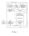
- Fig. 1 is a block diagram of a processor system according to one embodiment of the present invention.
- the processor system of Fig. 1 has a program ROM 1 for storing micro codes, an instruction decoder 2 for decoding instructions included in the micro codes, a program RAM 3 for storing the updated micro codes in which errors in the micro codes has been revised, an ROM address register 4 for storing addresses indicative of errors in the micro codes stored in the program RAM 1, a forced branch destination PC register 6 for storing a branch destination address when the micro codes include errors, an address comparator 7 for detecting whether the address stored in the address register 4 coincide with the program counter 5, a selector 8 for changing the program counter 5 into the branch destination address when both addresses coincide with each other, a micro computer IF unit 9 (an external IF unit) for transferring data for outside.
- a program ROM 1 for storing micro codes
- an instruction decoder 2 for decoding instructions included in the micro codes
- a program RAM 3 for storing the updated micro codes in which errors in the micro codes has been revised
- the instruction decoder 2 the ROM address register 4, the forced branch destination register 6 and the micro computer IF unit 6 are connected to a common data bus 10.
- Fig. 1 All the constituents of Fig. 1 may be contained in the one chip IC. Or a chip for the processor may be provided separate from a chip for a peripheral memory. In the case of providing separate chips, the processor has, for example, the instruction decoder 2 of Fig. 1, the ROM address register 4, the program counter 5, the forced branch destination register 6, the address comparator 7, the selector 8 and the micro computer IF 9.
- Fig. 2 is a flowchart showing processing operations of the processor system of Fig. 1. Hereinafter, the processing operations of this embodiment will be described with reference to Figs. 1 and 2. It is assumed that the micro codes in the program ROM 1 include a plurality of errors.
- the ROM address indicative of an error location at first time is stored in the ROM address register 4 from outside via the micro computer IF unit and a data bus 10.
- the address of the program RAM 3 in which the updated micro codes are stored is stored in the forced branch destination PC register from outside via the micro computer IF unit 9 and the data bus 10 (step S1).
- step S2 Instructions are read out from the program ROM 1 by setting the program counter 5 as an address, the instruction is decoded by the instruction decoder 2, and the instruction is executed (step S3).
- the address comparator 7 detects whether or not the program counter 5 coincides with the ROM address stored in the ROM address register 4 (step S4). If not coincided, the processings of steps S2 and S3 are repeated.
- the selector 8 changes the program counter 5 into the forced branch destination address stored in the forced branch destination PC register 6 (step S5).
- the forced branch destination address indicates the updated micro codes in the program RAM 3. Therefore, instead of the erroneous micro codes in the program ROM 1, the updated micro codes in the program RAM 3 are executed.
- the ROM address register 4 stores the address indicative of a next erroneous location of the micro codes in the program ROM 1. Similarly, the addresses of the updated micro codes in the program RAM 3 are stored in the forced branch destination PC register (S6). Subsequently, the processings of steps S2-S6 are repeated.
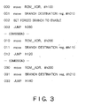
- Fig. 3 is a diagram showing one example of such kind of instruction strings.
- the program counter 5 when the program counter 5 is "000", the address "100" is stored in the ROM address register 4.
- the program counter 5 becomes "001” the address "10” is stored in the forced branch destination PC register 6.
- the program counter 5 becomes "002” the forced branch is allowed.
- the program counter 6 branches to the address "80" to execute the updated program.
- a plurality of addresses can be repeatedly stored via the data bus 10 in the ROM address register 4 and the forced branch destination PC register 6. Because of this, even if the micro codes in the program ROM 1 include a plurality of errors, it is possible to execute the updated micro codes corresponding to the errors, without increasing the circuit size, thereby improving maintainability of the program.
- the processor system of Fig. 1 can be used even to the debug of the program ROM 1.
- the debug is carried out by the instruction of the host computer connected to the micro computer IF.
- the debug program is stored from the host computer 1, via the micro computer IF, into the program RAM 3 (step S11). Subsequently, a head address for performing the debug of the program ROM 1 is stored from the host computer 11, via the micro computer IF, into the ROM address register 4. Similarly, the branch destination address at debug time (in this case, the head address of the debug program in the program RAM 3) is stored in the forced branch destination PC register 6 (step S12).
- step S13 execution of the program in the program ROM 1 is begun.
- step S14 execution of the program in the program ROM 1 is begun.
- the processing for transferring the value of an arbitrary memory and register via the micro computer IF, to the host computer 11 is carried out. Therefore, it is possible to perform the debug with regard to an arbitrary address range in the program ROM 1 (step S15).
- the debug program it is possible to store a new value in the ROM address register 4 and the forced branch destination PC register 6, and to continuously perform the debug with regard to a plurality of locations in the program ROM 1.
- step S16 it is determined whether or not the debug processings are finished. If determined to be finished, the processings of Fig. 4 are ended. If determined not to be finished, indirect addressing or return using stack is performed in the debug program, in order to return to the processings of the original program ROM 1 (step S17). Hereinafter, the processings of steps S13-S16 are repeated.
- steps S11-S14 are the same.
- the ROM address register 4 is incremented in the debug program.
- the processings after steps S13 are repeated.
Landscapes
- Engineering & Computer Science (AREA)
- Computer Hardware Design (AREA)
- Theoretical Computer Science (AREA)
- Quality & Reliability (AREA)
- Physics & Mathematics (AREA)
- General Engineering & Computer Science (AREA)
- General Physics & Mathematics (AREA)
- Debugging And Monitoring (AREA)
- Stored Programmes (AREA)
- Hardware Redundancy (AREA)
Applications Claiming Priority (2)
| Application Number | Priority Date | Filing Date | Title |
|---|---|---|---|
| JP2002285740 | 2002-09-30 | ||
| JP2002285740A JP2004126658A (ja) | 2002-09-30 | 2002-09-30 | プロセッサシステム |
Publications (2)
| Publication Number | Publication Date |
|---|---|
| EP1403768A2 true EP1403768A2 (de) | 2004-03-31 |
| EP1403768A3 EP1403768A3 (de) | 2007-05-02 |
Family
ID=31973404
Family Applications (1)
| Application Number | Title | Priority Date | Filing Date |
|---|---|---|---|
| EP03021630A Withdrawn EP1403768A3 (de) | 2002-09-30 | 2003-09-25 | Prozessorsystem, Prozessor und Arithmetik- Verarbeitungsverfahren |
Country Status (4)
| Country | Link |
|---|---|
| US (1) | US7203867B2 (de) |
| EP (1) | EP1403768A3 (de) |
| JP (1) | JP2004126658A (de) |
| CN (1) | CN1270249C (de) |
Families Citing this family (6)
| Publication number | Priority date | Publication date | Assignee | Title |
|---|---|---|---|---|
| JP2008015792A (ja) * | 2006-07-06 | 2008-01-24 | Fujitsu Ltd | Romパッチ処理方法およびromパッチ装置 |
| US8359522B2 (en) | 2007-05-01 | 2013-01-22 | Texas A&M University System | Low density parity check decoder for regular LDPC codes |
| CN101923495B (zh) * | 2009-06-10 | 2012-11-14 | Tcl集团股份有限公司 | 一种嵌入式容错系统及其容错方法 |
| NO332162B1 (no) * | 2009-12-21 | 2012-07-09 | Cisco Systems Int Sarl | Anordning og fremgangsmate for a filtrere mediapakker |
| WO2018235403A1 (ja) * | 2017-06-23 | 2018-12-27 | 日立オートモティブシステムズ株式会社 | 電子制御装置 |
| CN119402195B (zh) * | 2025-01-02 | 2025-06-20 | 山东航天人工智能安全芯片研究院 | 一种兼顾安全性与灵活性的密码协处理器架构及工作方法 |
Family Cites Families (11)
| Publication number | Priority date | Publication date | Assignee | Title |
|---|---|---|---|---|
| US5357627A (en) * | 1989-03-28 | 1994-10-18 | Olympus Optical Co., Ltd. | Microcomputer having a program correction function |
| TW231343B (de) * | 1992-03-17 | 1994-10-01 | Hitachi Seisakusyo Kk | |
| JPH05298462A (ja) | 1992-04-23 | 1993-11-12 | Sony Corp | 電子装置 |
| JPH0744419A (ja) * | 1993-08-03 | 1995-02-14 | Nec Ic Microcomput Syst Ltd | マイコン開発支援装置 |
| JPH0895946A (ja) | 1994-09-22 | 1996-04-12 | Nec Corp | マイクロコンピュータ |
| JPH08166877A (ja) * | 1994-12-13 | 1996-06-25 | Olympus Optical Co Ltd | 修正プログラムの実行可能なワンチップマイクロコンピュータ及びrom修正可能なマイクロコンピュータ |
| US6023758A (en) * | 1995-05-25 | 2000-02-08 | Matsushita Electric Industrial Co., Ltd. | Method and processor for changing program by replacing instruction stored in ROM with predetermined value to be interpreted as an instruction |
| JPH09319727A (ja) * | 1996-05-31 | 1997-12-12 | Hitachi Ltd | データプロセッサ及びデータ処理システム |
| TW400469B (en) * | 1997-07-08 | 2000-08-01 | Winbond Electronics Corp | Device capable of fixing programs in embedded microprocessor |
| CN1088868C (zh) | 1997-08-08 | 2002-08-07 | 华邦电子股份有限公司 | 可修补嵌入式微处理器系统中的程序的装置 |
| US6973522B1 (en) * | 1999-08-10 | 2005-12-06 | Pentax Corporation | Microcomputer with program-revision ability |
-
2002
- 2002-09-30 JP JP2002285740A patent/JP2004126658A/ja not_active Abandoned
-
2003
- 2003-09-25 EP EP03021630A patent/EP1403768A3/de not_active Withdrawn
- 2003-09-26 US US10/670,233 patent/US7203867B2/en not_active Expired - Lifetime
- 2003-09-30 CN CNB03127238XA patent/CN1270249C/zh not_active Expired - Fee Related
Also Published As
| Publication number | Publication date |
|---|---|
| CN1270249C (zh) | 2006-08-16 |
| EP1403768A3 (de) | 2007-05-02 |
| US7203867B2 (en) | 2007-04-10 |
| US20040153829A1 (en) | 2004-08-05 |
| JP2004126658A (ja) | 2004-04-22 |
| CN1497460A (zh) | 2004-05-19 |
Similar Documents
| Publication | Publication Date | Title |
|---|---|---|
| US6745278B2 (en) | Computer capable of rewriting an area of a non-volatile memory with a boot program during self mode operation of the computer | |
| US20060026415A1 (en) | Method of updating a portion BIOS | |
| US5600807A (en) | Programmable controller capable of updating a user program during operation by switching between user program memories | |
| EP0640916A2 (de) | Mikrorechner | |
| EP1403768A2 (de) | Prozessorsystem, Prozessor und Arithmetik- Verarbeitungsverfahren | |
| US6925522B2 (en) | Device and method capable of changing codes of micro-controller | |
| EP0577393B1 (de) | Verfahren zur Programmausführung | |
| US20010052114A1 (en) | Data processing apparatus | |
| KR100355630B1 (ko) | 롬 정정 유닛을 구비하는 컴퓨터 시스템 | |
| JP3358214B2 (ja) | 電子装置 | |
| CN118295669B (zh) | 一种确定全局偏移表的方法、装置及电子设备 | |
| US20100125720A1 (en) | Instruction mode identification apparatus and method | |
| JPH0546378A (ja) | プログラムの修正処理方法 | |
| US7281166B1 (en) | User-customizable input error handling | |
| JP2003509769A (ja) | 静的記憶装置内のマイクロ命令を修正するための方法及び装置 | |
| JP2733692B2 (ja) | Rom装置 | |
| JP3575052B2 (ja) | 電子装置 | |
| JPH1165622A (ja) | プログラマブルコントローラ | |
| JPH01113835A (ja) | 情報処理装置における記憶障害回避方式 | |
| JPH03160524A (ja) | 情報処理装置 | |
| JP2003178596A (ja) | 半導体集積回路 | |
| JPH09185526A (ja) | デバッグ装置 | |
| JP2002091785A (ja) | プログラム変更装置 | |
| JPH06161516A (ja) | シーケンスプログラムのチェック方法 | |
| JPH06110707A (ja) | 高優先度割り込み方法及び該方法が採用されたマイクロプロセッサ |
Legal Events
| Date | Code | Title | Description |
|---|---|---|---|
| PUAI | Public reference made under article 153(3) epc to a published international application that has entered the european phase |
Free format text: ORIGINAL CODE: 0009012 |
|
| 17P | Request for examination filed |
Effective date: 20030925 |
|
| AK | Designated contracting states |
Kind code of ref document: A2 Designated state(s): AT BE BG CH CY CZ DE DK EE ES FI FR GB GR HU IE IT LI LU MC NL PT RO SE SI SK TR |
|
| AX | Request for extension of the european patent |
Extension state: AL LT LV MK |
|
| PUAL | Search report despatched |
Free format text: ORIGINAL CODE: 0009013 |
|
| AK | Designated contracting states |
Kind code of ref document: A3 Designated state(s): AT BE BG CH CY CZ DE DK EE ES FI FR GB GR HU IE IT LI LU MC NL PT RO SE SI SK TR |
|
| AX | Request for extension of the european patent |
Extension state: AL LT LV MK |
|
| 17Q | First examination report despatched |
Effective date: 20071122 |
|
| AKX | Designation fees paid |
Designated state(s): DE FR GB |
|
| STAA | Information on the status of an ep patent application or granted ep patent |
Free format text: STATUS: THE APPLICATION IS DEEMED TO BE WITHDRAWN |
|
| 18D | Application deemed to be withdrawn |
Effective date: 20080603 |