EP1401102A2 - Programmierbare Halbleiterschaltung mit universellen Logikmodulen mit Multiplexern - Google Patents
Programmierbare Halbleiterschaltung mit universellen Logikmodulen mit Multiplexern Download PDFInfo
- Publication number
- EP1401102A2 EP1401102A2 EP03019021A EP03019021A EP1401102A2 EP 1401102 A2 EP1401102 A2 EP 1401102A2 EP 03019021 A EP03019021 A EP 03019021A EP 03019021 A EP03019021 A EP 03019021A EP 1401102 A2 EP1401102 A2 EP 1401102A2
- Authority
- EP
- European Patent Office
- Prior art keywords
- terminals
- inverter
- terminal
- realized
- connection
- Prior art date
- Legal status (The legal status is an assumption and is not a legal conclusion. Google has not performed a legal analysis and makes no representation as to the accuracy of the status listed.)
- Withdrawn
Links
Images







Classifications
-
- H—ELECTRICITY
- H03—ELECTRONIC CIRCUITRY
- H03K—PULSE TECHNIQUE
- H03K19/00—Logic circuits, i.e. having at least two inputs acting on one output; Inverting circuits
- H03K19/02—Logic circuits, i.e. having at least two inputs acting on one output; Inverting circuits using specified components
- H03K19/173—Logic circuits, i.e. having at least two inputs acting on one output; Inverting circuits using specified components using elementary logic circuits as components
- H03K19/1733—Controllable logic circuits
- H03K19/1737—Controllable logic circuits using multiplexers
Definitions
- the present invention relates to a programmable semiconductor device including universal logic modules.
- a logic cell formed by a plurality of kinds of universal logic modules is provided. Then, the user performs a connection operation upon the logic cell to realize a desired user logic circuit.
- FPGA field programmable gate array
- a logic cell is constructed by first universal logic modules serving as two-input, one-output multiplexers, second universal logic modules serving as inverters and a third universal logic module serving as a two-input, one-output multiplexer.
- the third universal logic module has the same configuration as the universal logic modules except that an inverter having a large current driving ability is provided.
- various kinds of user logic circuits can be made by the user using the first universal logic modules. This will be explained later in detail.
- the number of second universal logic modules may be increased.
- the ratio of the first universal logic modules, the second universal logic modules and the third universal logic modules is inappropriate due to the increased number of the second universal logic modules, the number of unused logic modules may be increased, which would increase a wasted area of the logic cell.
- a user delay circuit can be realized by connecting a plurality of the second universal logic modules in series. In this case, however, long connections are required between the series of the second universal logic modules, so that a delay time of the user delay circuit is increased.
- a logic module of a programmable semiconductor device is constructed by first, second, third, fourth and fifth terminals, a first transfer gate connected between the first and fourth terminals, a second transfer gate connected between the second and fourth terminals, and an inverter connected between the third and fifth terminals.
- the first and second transfer gates are controlled by voltages at the third and fifth terminals, so that one of the first and second transfer gates is turned 0N and the other of the first and second transfer gates is turned OFF.
- a logic module of a programmable semiconductor device is constructed by: first, second, third, fourth, fifth, sixth and seventh terminals; first and second connection/non-connection nodes capable of being either in a connection state or in a non-connection state; a first inverter connected between the first terminal and the first connection/non-connection terminal; a second inverter connected between the third terminal and the second connection/non-connection terminal; a third inverter connected between the fifth and seventh terminals; a first transfer gate connected between the first connection/non-connection node and the sixth terminal; and a second transfer gate connected between the second connection/non-connection node and the sixth terminal.
- the first and second transfer gates are controlled by voltages at the fifth and seventh terminals so that one of the first and second transfer gates is turned 0N and the other of the first and second transfer gates is turned OFF.
- a user inverter using one of the first, second and third inverters can be realized without the first and second transfer gates.
- a logic cell is constructed by universal logic modules X1 and X2 serving as two-input, one-output multiplexers, universal logic modules Y1 and Y2 serving as inverters and a universal logic module Z serving as a two-input, one-output multiplexer.
- the universal logic module Z has the same configuration as the universal logic modules X1 and X2 except that an inverter having a large current driving ability is provided.
- the logic cell of Fig. 1 has twenty terminals T1 through T20. Therefore, the user performs a connection operation upon all or some of the terminals T1 through T20, thus completing a desired user logic circuit.
- the universal logic module X1 is constructed by three CMOS inverters 1, 2 and 3 and two transfer gates 4 and 5 each formed by a P-channel MOS transistor and an N-channel MOS transistor.
- the transfer gates 4 and 5 are controlled by a voltage at the terminal T5 and the output voltage of the inverter 3, so that one of the transfer gates 4 and 5 is turned 0N and the other is turned OFF.
- Various kinds of user logic circuits can be made by the user using the universal logic module X1 as illustrated in Figs. 2A, 2B, 2C and 2D.
- the terminal T1 is fixed at "0" (low level), and the terminals T2 and T4 are open. Also, input signals A and B are supplied to the terminals T3 and T5, respectively, and an output signal Q is obtained from the terminal T6. Thus, a NAND circuit is realized.
- the terminal T3 is fixed at "1" (high level), and the terminal T2 and T4 are open. Also, input signals A and B are supplied to the terminals T1 and T5, respectively, and an output signal Q is obtained from the terminal T6. Thus, a NOR circuit is realized.
- Fig. 2D the terminals T1 and T4 are short-circuited, and the terminal T2 is open. Also, input signals A and B are supplied to the terminals T3 and T5, respectively, and an output signal Q is obtained from the terminal T6. Thus, an exclusive NOR circuit is realized.
- a user inverter may be realized by the user using the universal logic module X1 or X2.
- the terminal T5 is fixed at "0" (low level), and the terminals T2, T3 and T4 are open.
- an input signal A is supplied to the terminal T1
- an output signal Q is obtained from the terminal T6.
- the universal logic modules Y1 and Y2 are provided in the logic cell of Fig. 1 specialized for forming user inverters.
- the number of the universal logic modules such as Y1 and Y2 may be increased.
- the ratio of universal logic modules such as X1 and X2 universal logic modules such as Y1 and Y2 and universal logic modules such Z is inappropriate due to the increased number of the universal logic modules such as Y1 and Y2, the number of unused logic modules may be increased, which world increase a wasted area of the logic cell.
- a user delay circuit can be realized by connecting a plurality of the universal logic modules such as Y1 and Y2 in series. In this case, however, long connections are required between the series of the universal logic modules such as Y1 and Y2, so that a delay time of the user delay circuit is increased.
- Fig. 4 which illustrates an embodiment of the programmable semiconductor device according to the present invention
- the universal logic modules X1 and X2 of Fig. 1 are replaced by universal logic modules X1' and X2', respectively.
- a terminal T21 (T22) and connection/non-connection nodes N1 and N2 (N3 and N4) are added to the elements of the universal logic module X1 (X2) of Fig. 1.
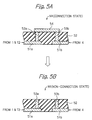
- connection/non-connection node N1 will be explained next with reference to Figs. 5A and 5B, which are partial cross-sectional views of the programmable semiconductor device of Fig. 4.
- conductive layers 51a and 51b are connected to the inverter 1 (the terminal T2) and the transfer gate 4, respectively.
- an insulating layer 52 is formed on the conductive layers 51a and 51b, and via structures 53a and 53b are formed through the insulating layer 52 on the conductive layers 51a and 51b, respectively.
- a conductive layer 54 is formed on the via structures 53a and 53b, so that the conductive layer 51a is electrically connected to the conductive layer 51b, i.e., the node N1 is in a connection state.
- the entirety of the conductive layer 54 is removed as illustrated in Fig. 5B, so that the conductive layer 51a is electrically disconnected from the conductive layer 51b, i.e., the node N1 is in a non-connection state.
- the conductive layer 51a is electrically disconnected from the conductive layer 51b, i.e., the node N1 is in a non-connection state.
- a part of the conductive layer 54 can be removed.
- the node N1 (N2, N3 and N4) can be either in a connection state or in a non-connection state.
- the user logic circuits as illustrated in Figs. 2A, 2B, 2C and 2D can be realized by the user using the universal logic module X1' under the condition that the nodes N1 and N2 are in a connection state and the terminal T21 is open, in the same way as in the universal logic module X1.
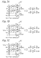
- inverters and delay circuits can be made by the user using the universal logic module X1' as illustrated in Figs. 6A, 6B, 6C, 7A, 7B, 7C, 8, 9, 10A, 10B, 10C, 11A, 11B and 11C.
- One inverter is realized by the universal logic module X1' as illustrated in Figs. 6A, 6B and 6C.
- the terminal T3 is fixed at "0" ( low level) or "1" (high level), and the terminals T4, T5, T6 and T21 are open. Also, an input signal A is supplied to the terminal T1, and an output signal Q1 is obtained from the terminal T2. Further, the node N1 is in a non-connection state, while the node N2 is in a connection state. Thus, one inverter using the inverter 1 is realized. In this case, since no transfer gate is present between the terminals T1 and T2, the realized inverter has a higher current driving ability and a smaller delay time as compared with an inverter realized by the universal logic module X1 of Fig. 1.
- the terminal T1 is fixed at "0" (low level) or "1" (high level), and the terminals T2, T5, T6 and T21 are open. Also, an input signal B is supplied to the terminal T3, and an output signal Q2 is obtained from the terminal T4. Further, the node N1 is in a connection state, while the node N2 is in a non-connection state. Thus, one inverter using the inverter 2 is realized. In this case, since no transfer gate is present between the terminals T3 and T4, the realized inverter has a higher current driving ability and a smaller delay time as compared with an inverter realized by the universal logic module X1 of Fig. 1.
- the terminals T1 and T3 are fixed at "0" (low level) or "1" (high level), and the terminals T2, T4, and T6 are open. Also, an input signal C is supplied to the terminal T5, and an output signal Q3 is obtained from the terminal T21. Further, the nodes N1 and N2 are in a non-connection state. Thus, one inverter using the inverter 3 is realized. In this case, since no transfer gate is present between the terminals T5 and T21, the realized inverter has a higher current driving ability and a smaller delay time as compared with an inverter realized by the universal logic module X1 of Fig. 1.
- Fig. 7A the terminals T5, T6 and T21 are open. Also, input signals A and B are supplied to the terminals T1 and T3, respectively, and output signals Q1 and Q2 are obtained from the terminals T2 and T4, respectively. Further, the nodes N1 and N2 are in a non-connection state. Thus, two inverters using the inverters 1 and 2 are realized. In this case, since no transfer gate is present between the terminals T1 and T2 and between the terminals T3 and T4, each of the realized inverters has a higher current driving ability and a smaller delay time as compared with an inverter realized by the universal logic module X1 of Fig. 1.
- the terminal T3 is fixed at "0" (low level) or "1" (high level), and the terminals T4 and T6 are open. Also, input signals A and C are supplied to the terminals T1 and T5, respectively, and output signals Q1 and Q3 are obtained from the terminals T2 and T21, respectively. Further, the node N1 is in a non-connection state, while the node N2 is in a connection state. Thus, two inverters using the inverters 1 and 3 are realized.
- each of the realized inverters has a higher current driving ability and a smaller delay time as compared with an inverter realized by the universal logic module X1 of Fig. 1.
- the terminal T1 is fixed at "0" (low level) or "1" (high level), and the terminals T2 and T6 are open. Also, input signals B and C are supplied to the terminals T3 and T5, respectively, and output signals Q2 and Q3 are obtained from the terminals T4 and T21, respectively. Further, the node N1 is in a connection state, while the node N2 is in a non-connection state. Thus, two inverters using the inverters 2 and 3 are realized.
- each of the realized inverters has a higher current driving ability and a smaller delay time as compared with an inverter realized by the universal logic module X1 of Fig. 1.
- the terminal T6 is open. Also, input signals A, B and C are supplied to the terminals T1, T3 and T5, respectively, and output signals Q1, Q2 and Q3 are obtained from the terminals T2, T4 and T21, respectively. Further, the nodes N1 and N2 are in a non-connection state. Thus, three inverters using the inverters 1, 2 and 3 are realized. In this case, since no transfer gate is present between the terminals T1 and T2, between the terminals T3 and T4 and between the terminals T5 and T21, each of the realized inverters has a higher current driving ability and a smaller delay time as compared with an inverter realized by the universal logic module X1 of Fig. 1.
- One inverter formed by three inverter elements is realized by the universal logic module X1' as illustrated in Fig. 9.
- the terminal T2 is connected to the terminal T3, and the terminal T4 is connected to the terminal T5. Also, the terminal T6 is open. Also, an input signal A is supplied to the terminal T1, and an output signal Q3 is obtained from the terminal T21. Further, the nodes N1 and N2 are in a non-connection state. Thus, one inverter using the series of the inverters 1, 2 and 3 is realized. In this case, since no transfer gate is present between the terminals T1 and T21, the realized inverter has a higher current driving ability and a smaller delay time as compared with an inverter realized by the universal logic module X1 of Fig. 1.
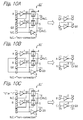
- a delay circuit (buffer circuit) is realized by the universal logic module X1' as illustrated in Figs. 10A, 10B and 10C.
- the terminal T2 is connected to the terminal T3, and the terminals T5, T6 and T21 are open. Also, an input signal A is supplied to the terminal T1, and an output signal Q2 is obtained from the terminal T4. Further, the nodes N1 and N2 are in a non-connection state. Thus, a delay circuit using the inverters 1 and 2 is realized. In this case, since no transfer gate is present between the terminals T1 and T4, the realized delay circuit has a high current driving ability.
- the terminal T2 is connected to the terminal T5.
- the terminal T3 is fixed at "0" (low level) or "1" (high level), and the terminals T4 and T6 are open.
- an input signal A is supplied to the terminal T1
- an output signal Q3 is obtained from the terminal T21.
- the node N1 is in a non-connection state, while the node N2 is in a connection state.
- a delay circuit using the inverters 1 and 3 is realized. In this case, since no transfer gate is present between the terminals T1 and T3, the realized delay circuit has a high current driving ability.
- the terminal T4 is connected to the terminal T5.
- the terminal T1 is fixed at "0" (low level) or "1" (high level), and the terminals T2 and T6 are open.
- an input signal B is supplied to the terminal T3, and an output signal Q3 is obtained from the terminal T21.
- the node N1 is in a connection state, while the node N2 is in a non-connection state.
- a delay circuit using the inverters 2 and 3 is realized. In this case, since no transfer gate is present between the terminals T3 and T21, the realized delay circuit has a high current driving ability.
- a delay circuit (buffer circuit) as well as an inverter are realized by the universal logic module X1' as illustrated in Figs. 10A, 10B and 10C.
- the terminal T2 is connected to the terminal T3, and the terminals T6 and T21 are open. Also, input signals A and C are supplied to the terminals T1 and T5, respectively, and output signals Q2 and Q3 are obtained from the terminals T4 and T21, respectively. Further, the nodes N1 and N2 are in a non-connection state. Thus, a delay circuit using the inverters 1 and 2 and an inverter using the inverter 3 are realized. In this case, since no transfer gate is present between the terminals T1 and T4 and between the terminals T5 and T21, each of the realized delay circuit and inverter has a high current driving ability.
- the terminal T2 is connected to the terminal T5. Also, the terminal T6 is open. Also, input signals A and B are supplied to the terminals T1 and T3, respectively, and output signals Q2 and Q3 are obtained from the terminals T4 and T21, respectively. Further, the node N1 is in a non-connection state, while the node N2 is in a connection state. Thus, a delay circuit using the inverters 1 and 3 and an inverter using the inverter 2 are realized. In this case, since no transfer gate is present between the terminals T1 and T2 and between the terminals T3 and T4, each of the realized delay circuit and inverter has a high current driving ability.
- the terminal T4 is connected to the terminal T5.
- the terminal T6 is open.
- input signals A and B are supplied to the terminals T1 and T3, respectively, and output signals Q1 and Q3 are obtained from the terminals T2 and T21, respectively.
- the node N1 is in a connection state, while the node N2 is in a non-connection state.
- a delay circuit using the inverters 2 and 3 and an inverter using the inverter 1 are realized.
- each of the realized delay circuit and inverter has a high current driving ability.
- a realized user inverter can have various current driving abilities and delay times.
- the present invention can be applied to a universal logic module as illustrated in Figs. 12A, 12B, 12C and 12D.
- Fig. 12A the inverters 1 and 2, the terminals T1 and T2 and the nodes N1 and N2 are removed from the universal logic module X1' of Fig. 4.
- Fig. 12B the terminals T1 and T2 and the nodes N1 and N2 are removed from the universal logic module X1' of Fig. 4.
- the inverter 2 the terminals T1 and T2 and the node N1 and N2 are removed from the universal logic module X1' of Fig. 4.
- Fig. 12A the inverters 1 and 2 and the terminals T1 and T2 and the nodes N1 and N2 are removed from the universal logic module X1' of Fig. 4.
- Fig. 12C the inverter 2
- the terminals T1 and T2 and the node N1 and N2 are removed from the universal logic module X1' of Fig. 4.
- the inverter 1, the terminals T1 and T2 and the nodes N1 and N2 are removed from the universal logic module X1' of Fig. 4. That is, in Figs. 12A, 12B, 12C and 12D, at least one user inverter using the inverter 3 can be realized.
Landscapes
- Physics & Mathematics (AREA)
- Engineering & Computer Science (AREA)
- Computer Hardware Design (AREA)
- Computing Systems (AREA)
- General Engineering & Computer Science (AREA)
- Mathematical Physics (AREA)
- Pulse Circuits (AREA)
- Logic Circuits (AREA)
- Semiconductor Integrated Circuits (AREA)
- Design And Manufacture Of Integrated Circuits (AREA)
- Electronic Switches (AREA)
Applications Claiming Priority (2)
| Application Number | Priority Date | Filing Date | Title |
|---|---|---|---|
| JP2002275376 | 2002-09-20 | ||
| JP2002275376A JP2004112653A (ja) | 2002-09-20 | 2002-09-20 | 半導体装置 |
Publications (2)
| Publication Number | Publication Date |
|---|---|
| EP1401102A2 true EP1401102A2 (de) | 2004-03-24 |
| EP1401102A3 EP1401102A3 (de) | 2009-09-23 |
Family
ID=31944609
Family Applications (1)
| Application Number | Title | Priority Date | Filing Date |
|---|---|---|---|
| EP03019021A Withdrawn EP1401102A3 (de) | 2002-09-20 | 2003-08-21 | Programmierbare Halbleiterschaltung mit universellen Logikmodulen mit Multiplexern |
Country Status (3)
| Country | Link |
|---|---|
| US (1) | US6943584B2 (de) |
| EP (1) | EP1401102A3 (de) |
| JP (1) | JP2004112653A (de) |
Families Citing this family (1)
| Publication number | Priority date | Publication date | Assignee | Title |
|---|---|---|---|---|
| JP4471776B2 (ja) * | 2004-08-16 | 2010-06-02 | Necエレクトロニクス株式会社 | 半導体装置、半導体装置の製造方法 |
Family Cites Families (3)
| Publication number | Priority date | Publication date | Assignee | Title |
|---|---|---|---|---|
| US5684412A (en) * | 1995-08-18 | 1997-11-04 | Chip Express (Israel) Ltd. | Cell forming part of a customizable logic array |
| JPH09148916A (ja) * | 1995-11-24 | 1997-06-06 | Nec Corp | 半導体集積回路 |
| JP3555080B2 (ja) * | 2000-10-19 | 2004-08-18 | Necエレクトロニクス株式会社 | 汎用ロジックモジュール及びこれを用いたセル |
-
2002
- 2002-09-20 JP JP2002275376A patent/JP2004112653A/ja active Pending
-
2003
- 2003-08-08 US US10/636,636 patent/US6943584B2/en not_active Expired - Lifetime
- 2003-08-21 EP EP03019021A patent/EP1401102A3/de not_active Withdrawn
Also Published As
| Publication number | Publication date |
|---|---|
| EP1401102A3 (de) | 2009-09-23 |
| US20040056688A1 (en) | 2004-03-25 |
| JP2004112653A (ja) | 2004-04-08 |
| US6943584B2 (en) | 2005-09-13 |
Similar Documents
| Publication | Publication Date | Title |
|---|---|---|
| US20090002044A1 (en) | Master-slave type flip-flop circuit | |
| EP1199802B1 (de) | Logisches Allzweckmodul und Zelle mit einem solchen Modul | |
| JPH08329822A (ja) | 信号経路選択用のスイッチ回路 | |
| JPH1139048A (ja) | 中間電位生成回路 | |
| EP0920132A1 (de) | Tristate-Ausgangsschaltung | |
| JP3814589B2 (ja) | スイッチ回路及びバススイッチ回路 | |
| EP1401102A2 (de) | Programmierbare Halbleiterschaltung mit universellen Logikmodulen mit Multiplexern | |
| JP2749185B2 (ja) | 複合論理回路 | |
| JP2009016891A (ja) | マスタスレーブ型フリップフロップ回路 | |
| US6100740A (en) | Circuit for selectively enabling one among a plurality of circuit alternatives of an integrated circuit | |
| JP3719242B2 (ja) | 半導体装置及び発振回路 | |
| JP2009021650A (ja) | マスタスレーブ型フリップフロップ回路 | |
| US7205795B2 (en) | Semiconductor device having universal logic cell | |
| US6603219B2 (en) | Semiconductor integrated circuit | |
| US7429872B2 (en) | Logic circuit combining exclusive OR gate and exclusive NOR gate | |
| JP2867253B2 (ja) | 3入力エクスクルシーブオアゲート | |
| JPH06311022A (ja) | 半導体論理回路装置 | |
| US7185307B2 (en) | Method of fabricating and integrated circuit through utilizing metal layers to program randomly positioned basic units | |
| KR0155322B1 (ko) | 인버터 기능을 갖는 프로그램이 가능한 양방향성 버퍼 | |
| JP2546398B2 (ja) | レベル変換回路 | |
| US20060119371A1 (en) | Semiconductor device and evaluation circuit for the same | |
| JP2000183725A (ja) | 半導体集積回路の構成方法 | |
| JP2004215019A (ja) | レベル変換機能付き入出力回路および半導体集積回路装置 | |
| JPH1187665A (ja) | 半導体集積回路 | |
| JPH09200040A (ja) | 半導体集積回路 |
Legal Events
| Date | Code | Title | Description |
|---|---|---|---|
| PUAI | Public reference made under article 153(3) epc to a published international application that has entered the european phase |
Free format text: ORIGINAL CODE: 0009012 |
|
| AK | Designated contracting states |
Kind code of ref document: A2 Designated state(s): AT BE BG CH CY CZ DE DK EE ES FI FR GB GR HU IE IT LI LU MC NL PT RO SE SI SK TR |
|
| AX | Request for extension of the european patent |
Extension state: AL LT LV MK |
|
| PUAL | Search report despatched |
Free format text: ORIGINAL CODE: 0009013 |
|
| AK | Designated contracting states |
Kind code of ref document: A3 Designated state(s): AT BE BG CH CY CZ DE DK EE ES FI FR GB GR HU IE IT LI LU MC NL PT RO SE SI SK TR |
|
| AX | Request for extension of the european patent |
Extension state: AL LT LV MK |
|
| 17P | Request for examination filed |
Effective date: 20100316 |
|
| AKX | Designation fees paid |
Designated state(s): DE FI FR GB IT SE |
|
| 17Q | First examination report despatched |
Effective date: 20100617 |
|
| RAP1 | Party data changed (applicant data changed or rights of an application transferred) |
Owner name: RENESAS ELECTRONICS CORPORATION |
|
| STAA | Information on the status of an ep patent application or granted ep patent |
Free format text: STATUS: THE APPLICATION HAS BEEN WITHDRAWN |
|
| 18W | Application withdrawn |
Effective date: 20101021 |