EP1394825A1 - MEMS-Kontaktanordnung und Mikro-Relais - Google Patents
MEMS-Kontaktanordnung und Mikro-Relais Download PDFInfo
- Publication number
- EP1394825A1 EP1394825A1 EP02405741A EP02405741A EP1394825A1 EP 1394825 A1 EP1394825 A1 EP 1394825A1 EP 02405741 A EP02405741 A EP 02405741A EP 02405741 A EP02405741 A EP 02405741A EP 1394825 A1 EP1394825 A1 EP 1394825A1
- Authority
- EP
- European Patent Office
- Prior art keywords
- contact
- flexible
- segment
- switching state
- mems
- Prior art date
- Legal status (The legal status is an assumption and is not a legal conclusion. Google has not performed a legal analysis and makes no representation as to the accuracy of the status listed.)
- Granted
Links
Images



Classifications
-
- H—ELECTRICITY
- H01—ELECTRIC ELEMENTS
- H01H—ELECTRIC SWITCHES; RELAYS; SELECTORS; EMERGENCY PROTECTIVE DEVICES
- H01H1/00—Contacts
- H01H1/0036—Switches making use of microelectromechanical systems [MEMS]
-
- H—ELECTRICITY
- H01—ELECTRIC ELEMENTS
- H01H—ELECTRIC SWITCHES; RELAYS; SELECTORS; EMERGENCY PROTECTIVE DEVICES
- H01H1/00—Contacts
- H01H1/12—Contacts characterised by the manner in which co-operating contacts engage
- H01H1/14—Contacts characterised by the manner in which co-operating contacts engage by abutting
- H01H1/24—Contacts characterised by the manner in which co-operating contacts engage by abutting with resilient mounting
-
- H—ELECTRICITY
- H01—ELECTRIC ELEMENTS
- H01H—ELECTRIC SWITCHES; RELAYS; SELECTORS; EMERGENCY PROTECTIVE DEVICES
- H01H1/00—Contacts
- H01H1/12—Contacts characterised by the manner in which co-operating contacts engage
- H01H1/36—Contacts characterised by the manner in which co-operating contacts engage by sliding
- H01H1/38—Plug-and-socket contacts
-
- H—ELECTRICITY
- H01—ELECTRIC ELEMENTS
- H01H—ELECTRIC SWITCHES; RELAYS; SELECTORS; EMERGENCY PROTECTIVE DEVICES
- H01H1/00—Contacts
- H01H1/50—Means for increasing contact pressure, preventing vibration of contacts, holding contacts together after engagement, or biasing contacts to the open position
- H01H1/52—Contacts adapted to act as latches
-
- H—ELECTRICITY
- H01—ELECTRIC ELEMENTS
- H01H—ELECTRIC SWITCHES; RELAYS; SELECTORS; EMERGENCY PROTECTIVE DEVICES
- H01H1/00—Contacts
- H01H1/0036—Switches making use of microelectromechanical systems [MEMS]
- H01H2001/0042—Bistable switches, i.e. having two stable positions requiring only actuating energy for switching between them, e.g. with snap membrane or by permanent magnet
-
- H—ELECTRICITY
- H01—ELECTRIC ELEMENTS
- H01H—ELECTRIC SWITCHES; RELAYS; SELECTORS; EMERGENCY PROTECTIVE DEVICES
- H01H1/00—Contacts
- H01H1/0036—Switches making use of microelectromechanical systems [MEMS]
- H01H2001/0042—Bistable switches, i.e. having two stable positions requiring only actuating energy for switching between them, e.g. with snap membrane or by permanent magnet
- H01H2001/0047—Bistable switches, i.e. having two stable positions requiring only actuating energy for switching between them, e.g. with snap membrane or by permanent magnet operable only by mechanical latching
-
- H—ELECTRICITY
- H01—ELECTRIC ELEMENTS
- H01H—ELECTRIC SWITCHES; RELAYS; SELECTORS; EMERGENCY PROTECTIVE DEVICES
- H01H59/00—Electrostatic relays; Electro-adhesion relays
- H01H59/0009—Electrostatic relays; Electro-adhesion relays making use of micromechanics
Definitions
- the invention relates to the field of micro-electromechanical Systems (MEMS), in particular according to a MEMS contact arrangement according to the preamble of claim 1 and to a MEMS switching device the preamble of claim 16.
- MEMS micro-electromechanical Systems
- MEMS contact arrangement and a Such MEMS switching device is for example from the published patent application DE 10040867 A1 known.
- a substrate parallel, i.e. laterally working Microswitch disclosed which by means of ion deep etching (DRIE, deep reactive ion etching) is made of a silicon substrate and three contact pieces includes. Two of the three contact pieces are fixed on the substrate (Fixessore). The other, movable contact piece is part of one part movable contact carrier.
- This contact carrier is parallel to the substrate bendable and fixed at its two ends on the substrate.
- the two Fixed contacts are with respect to the two ends of the movable contact carrier arranged asymmetrically so that the movable contact carrier two has stable positions (switching states). Has turned off the movable contact carrier in the form of a symmetrical antinode, when switched on the shape of an asymmetrical Antinode. When switched on, the movable contacts Contact piece the two fixed contacts. At least one electrostatic The drive is the movable contact carrier from a switching state switchable to the other switching state.
- the fixed contacts are solid and rigid. They are finger-shaped and in Rounded direction of the movable contact piece.
- the mobile Contact piece is, even when switched on, despite the flexibility of the Contact carrier rigid. Because that at its two ends on the substrate Fixed contact carrier must be able to withstand high pressure forces to exercise the fixed contacts. When creating the contacts between the movable Contact piece and the fixed contacts therefore come the three contact pieces immediately to rest, and there is a point-like contact for each fixed contact or linear contact with the movable line perpendicular to the substrate Contact piece, namely at the points of the first touch of the movable contact piece with the fixed contacts.
- Such a point-like or line-like perpendicular to the substrate Contact has a large electrical and thermal resistance, because the contact area or the number of contact points is very small.
- soiling of the contacting surfaces Increase contact resistance further, especially when switching small currents contamination, where there is no arc from the contact surfaces.
- the object of the invention is a micro-mechanical or micro-electromechanical (MEMS) contact arrangement and a micro-mechanical or micro-electromechanical (MEMS) switching device of the input to create the type mentioned, which does not have the disadvantages mentioned above exhibit. In particular, improved and reliable contacting is to be achieved become.
- MEMS micro-mechanical or micro-electromechanical
- the MEMS contact arrangement has at least a first one Contact piece and a second contact piece, at least one of the two contact pieces can be driven, and wherein the MEMS contact arrangement by means of the drivable contact piece between one first switching state and at least one second switching state switchable is, the two contact pieces in the first switching state of each other are separated and contacting each other in the second switching state are. It is characterized in that at least the first contact piece at least one flexible contact segment and a contact segment carrier has, and that the at least one flexible contact segment by means of at least the second contact piece during a switching operation of the first switching state in the second switching state and / or from the second switching state is elastically deformable in the first switching state.
- the at least one flexible contact segment is by means of at least one of the second contact piece in a switching process elastically deformable that the at least one flexible contact segment with the second contact piece in the second switching state at least one flat Touch area or a predeterminable plurality of touch points having.
- the effective one Size of contact areas and / or the number of contact points is increased, so that the electrical and / or thermal resistance the contact point is reduced or one provided with the contact arrangement Micro valve closes more tightly.
- the flexible contact segment in the second switching state is advantageous molded second contact piece. That means that in the second switching state the shape of the flexible contact segment in areas where the first and touch the second contact piece to the shape of the second contact piece is adjusted. Due to the elastic deformation that the flexible Contact segment experienced through the switching process is the shape of the flexible Contact segments in the first switching state differ from the shape of the flexible Contact segments in the second switching state. This ensures a safe, because large contact areas and / or many contact points Contact reached.
- the flexible contact segment and the second contact piece in the second switching state at least one area of contact, in the second Switching state of the second contact piece in the contact area of the first contact piece is enclosed. This will make because large-scale contact is achieved.
- the second contact piece opposite the flexible contact segment smoothly movable during a switching operation.
- This is advantageous both for switching operations from the first to the second as well as for switching operations from the second to the first switching state.
- When manufacturing and / or releasing a contact move the flexible contact segment and the second contact piece relative to each other while they are doing so touch. Due to the mutual friction of the two contact pieces Soiling of the contact pieces can be removed. This cleanses itself the contact arrangement automatically by switching operations. Clean contacts mean safe contacts. The reliability of contacting is thereby very high.
- This embodiment is particularly advantageous with electrical Applications and especially when currents are switched that do not generate an arc that has a contact cleaning effect could.
- the flexible contact segment due to its thin walls, flexible and elastic deformable.
- the flexible contact segment has at least one flexible section, the is so thin or narrow that it has flexibility.
- one of the flexible contact segment can be advantageous flexible section with a wall thickness between 1 ⁇ m and 60 ⁇ m, preferably between 5 ⁇ m and 25 ⁇ m. typically, The materials used then have a suitable flexibility and deformability on, but there is still sufficient breaking strength.
- the elastic deformations that a flexible section of a flexible Contact segments typically through the second contact piece at one Switching process experienced is advantageous at least on the order of magnitude the wall thickness of the flexible section of the flexible contact segment and / or in the range of 0.1 to 20 times, in particular 1 to 5 times the wall thickness of the flexible section of the flexible contact segment.
- At least the first contact piece is advantageously formed in one piece. This improves the producibility of the first contact piece, and the The stability and reliability of the first contact piece is particularly great.
- the flexible contact segment in addition to at least one flexible Section another base facing the contact segment carrier on.
- This base advantageously has a greater wall thickness than the at least one a flexible section of the flexible contact segment. This points the basis of less flexibility. For a base deformation requires more energy than to deform the at least one flexible one Section. The base is more stable than the flexible section. The base points greater electrical and / or thermal conductivity. For example heat can be dissipated better, and for short periods For large thermal loads, an increased heat capacity is an advantage. Improved contacting is realized.
- a further advantageous embodiment is characterized in that for the elastic deformation of the at least one flexible contact segment by means of at least the second contact piece at one Switching process from the first switching state to the second switching state or from the second switching state to the first switching state an insertion energy or an execution energy is to be applied, and that in the second switching state of the flexible contact segment a restraining force is exerted on the second contact piece, by what retention force a switching operation from the second switching state is difficult in the first switching state.
- a potential mountain must be overcome.
- the for Switching required energy is generally applied by a drive, by means of which the drivable contact piece is driven.
- the second switching state is a safe and good contact that supports the flexible contact piece due to the in it the deformation during the transition from the first to the second switching state stored deformation energy a compressive force on the second Contact piece.
- This pressure force can also be referred to as a retention force become.
- In the second switching state there can be a jamming connection exist between the two contact pieces.
- the flexible contact segment acts and the second contact piece in the manner of the push button principle together that the contact segment carrier has at least one additional has a stable position.
- the contact segment carrier is a monostable Is a switching element, it can be a bistable switching element (and a bistable contact arrangement) or a tristable switching element become. And from a bistable switchable contact segment carrier can become a tristably switchable switching element.
- the flexible contact segment has at least two, advantageously four, six or more elastic deformable contact fingers.
- These advantageously elongated and thin, advantageous cane-like curved segments are such shaped and arranged that each (or at least most) of the sub-segments touches the second contact piece in the second switching state. Thereby result in at least one (approximately) the number of sub-segments corresponding predeterminable number of contact points or a corresponding one Majority of contact surfaces. This ensures a safe contact achieved with low contact resistance.
- the angle ⁇ lies in one plane, which is perpendicular to the plane of the area of contact.
- those surfaces of the flexible contact segment and the second contact piece, those in the second switching state essentially parallel to one another are aligned and touch each other in the area of contact, are essentially up to an angle ⁇ in the first switching state 0 ° ⁇ ⁇ ⁇ 30 °, in particular 0 ° ⁇ ⁇ ⁇ 10 °, aligned parallel to each other.
- the angle ⁇ can advantageously additionally be at least 1 ° large, at least 2 ° large or at least 4 ° large. at a switching process from the first to the second and / or from the second in the surfaces mentioned rub against the first switching state, whereby contact deteriorating impurities can be removed. On In this way, a safe, large-area and self-cleaning contact is made achieved.
- this includes flexible contact segment a membrane-like section, which at a Switching process is deformed elastically.
- a membrane fits flat on the shape of the second contact piece and equalizes manufacturing tolerances out. Low contact resistance and reliable contacting can be achieved.
- a volume is enclosed with the first contact piece, which essentially with an electrically and thermally conductive, elastically deformable Filling is filled. This will make the electrical and / or thermal Conductivity of the flexible contact segment increased.
- a MEMS switching device for example a micro relay, which is an inventive Contact arrangement includes, has the above advantages.
- Fig. 1 shows schematically an inventive micro-electromechanical Relays (MEMS relays, micro relays) under supervision.
- MEMS relays micro-electromechanical Relays
- Such a MEMS relay is ion-etched (DRIE) made of a semiconductor material, preferably single crystal Silicon can be produced.
- DRIE ion-etched
- the linear dimension of such a MEMS switching device is typically of the order of 0.4 mm to 5 mm.
- the structures created using DRIE are mostly prismatic, with the Prism side faces are perpendicular to the surface of the substrate extend from which they are etched and optionally sacrificial layer technology were formed.
- the height of the prisms is typically from of the order of 50 ⁇ m to 500 ⁇ m.
- DE 10040867 A1 are further details on such and similar microswitches described. In order not to repeat this here, the disclosure content this text hereby expressly in the present description accepted.
- the MEMS relay shown in FIG. 1 has a first contact piece 1 second contact piece 2 and a third contact piece 3.
- the first contact 1 comprises a flexible contact segment 11 and one with the flexible Contact segment connected contact segment carrier 12.
- the contact segment carrier 12 is horizontal, that is perpendicular to the substrate normal bendable and has two stable positions. At both ends is the contact segment carrier 12 is fixed on the substrate.
- the relay In the first, position of the contact segment carrier represented by solid lines the relay is in a first switching state A, in which the relay is open: the contact pieces 2 and 3 are not conductive with each other connected.
- the contact segment carrier 12 can be driven into its second bistable Position in which the relay is in a second, closed position B: by means of the flexible contact segment 11, which has a metallic coating, they are also metallically coated contact pieces 2 and 3 conductive with each other connected.
- the relay By means of the drive 4 shown at the bottom right in FIG. 1 the relay can be switched back to the open switching state 2.
- a contact arrangement is shown schematically, which is similar that is shown in Fig. 1. However, it only has a first contact piece 1 and a second contact piece 2.
- the first contact piece 1 is formed in one piece and has a flexible contact segment 11 and a contact segment carrier 12 on.
- the latter can be designed, for example, as in FIG. 1.
- the flexible Contact segment 11 is membrane-like. It represents a thin wall represents that with the contact segment carrier 12 encloses a volume 114.
- the enclosed volume 114 is prism-like and is enclosed laterally, while it is not in the direction parallel to the substrate is enclosed.
- This volume not enclosed but enclosed 114 can be filled completely or partially with a conductive filling. Surface effects help fill the volume 114 remains.
- the filling for example, can be more likely have good electrical and / or good thermal conductivity.
- Filling is suitable, inter alia, for liquid metals, for example mercury, Indium, gallium or alloys of these metals, or also (electrical) conductive polymers, for example conjugated polymers. By means of such a Filled contact resistance can be achieved.
- the unfilled contact pieces already have good conductivity on, for example in the case of semiconducting materials by appropriate Doping.
- the flexible contact segment 11 (in supervision) about the shape of a letter "U", which is concavely bent at the bottom.
- the second switching state B becomes flexible Contact segment 11 through the front finger-shaped second Contact piece 2 elastically deformed.
- the flexible contact segment 11 is flexible and elastic deformable because it is thin-walled.
- the wall surfaces then typically have a thickness d from 1 ⁇ m to 60 ⁇ m; best results were obtained in the thickness range from 5 ⁇ m to 25 ⁇ m.
- the two have Contact pieces 1,2 a flat contact area 5 on. In the contact area 5, the shape of the flexible contact segment 1 1 of the shape of the second contact piece 2.
- the shape of the flexible contact segment 11 is different in the second switching state B. than in the first switching state A.
- In the contact area 5 is the second Contact piece 2 of the flexible contact segment 11 and thus of the first contact piece 1 enclosed flat.
- the shape of the two Contact pieces 1,2 a centering effect is still achieved, whereby Manufacturing tolerances can be compensated.
- FIG. 3a and 3b show a contact arrangement similar to that from FIG. 1 and Fig. 2a, b.
- the contact arrangement corresponds to that of FIG. 2, only that instead a second contact segment 2 has two contact pieces 2 and 3 become.
- Each of the two contact pieces 2 and 3 has the shape of a rounded Half of a split lengthwise, shown in Fig. 2a, b, finger-shaped contact piece.
- the above-mentioned sliding friction Self-cleaning effect is even stronger in this embodiment than in the embodiment of Fig. 2. Because for each of the contact pieces 2 and 3 results in a switch-on process (A to B) a clearly asymmetrical, laterally (not frontally) first point of contact with the flexible contact segment 1 1. Until then an end position of the contact pieces 1,2,3 is reached, there is a rubbing relative movement of the contact pieces 2 and 3 compared to the flexible contact segment 11.
- the design is rounded preferred the contact pieces without tips, because this makes electrical Field stress and peak effects can be avoided.
- the 4 is not membrane-like flexible contact segment 11 as in FIG. 2 shaped essentially symmetrically, but has an asymmetrical shape Shape in relation to the direction of mutual movement of the flexible Contact segment 11 and the second contact piece 2. This results as described in connection with Fig. 3, an intense friction of the second contact piece 2 with the flexible contact segment 11, which lead to the removal of any impurities in the contact area 5 can.
- Fig. 4a outlines the first switching state A.
- Fig. 4b shows a switching state during a switching process from A to B.
- the first contact piece 1 already contacts the second contact piece 2.
- the contact arrangement can be advantageous be dimensioned so that only the position shown in Fig. 4c is the end position, i.e. the switching state B.
- the flexible Contact segment 11 not only one contact point at the two ends of the membrane with the contact segment carrier 12, but additionally a further contact point that is not present in the first switching state A. 6 (or a touch pad 6). This results in a lower one Contact resistance.
- Possible contacting problems due to manufacturing tolerances can at least be reduced, among other things, that the contact piece that is driven is always one Residual mobility, usually due to a spring-like suspension. If one transfers the structure from FIG. 4 to the switching device from FIG. 1, then the first contact piece 1 the driven contact piece.
- Fig. 5 shows a further contact arrangement according to the invention, which the 3 and is described on the basis thereof.
- the flexible Contact segment 11 has in Fig. 5 except a membrane-like flexible Section another base 113.
- the flexible contact segment 11 has approximately the shape of an isosceles triangle, with the Base side of the triangle from the second contact piece 2 and the third Contact piece 3 faces away and is formed by the base 113. It's the first switching state A shown. That of the flexible contact segment 11th enclosed volume 114 can be used as needed, as related to Fig. 2 described to be filled with a filling.
- the flexible contact segment 11 in particular on the Contact pieces 2 and 3 facing side (tip of the triangle), rounded (not shown).
- the flexible section of the flexible contact segment 11 elastically deformed, and there is a sliding motion between the flexible contact segment 11 and Contact pieces 2 and 3.
- the base 113 of the flexible contact segment 11 increases the conductivity the contact arrangement. Electrical and / or thermal resistances will be thereby reduced. And a larger heat capacity is realized.
- FIG. 6 shows a contact arrangement which largely corresponds to that from FIG. 5.
- the contact segment 11 can optimally contact the contact pieces Nestle 2 and 3
- Fig. 7 is a contact arrangement with a first contact piece 1 and shown second contact piece 2, in which the two contact pieces 1.2 interact in the manner of a plug-socket pair.
- the second Contact piece 2 has a nose that is approximately the shape of a rounded one Rectangle, which also has a small waist.
- the first contact piece 1 contains the contact segment carrier 12 another flexible contact segment 11, the two flexible contact fingers 111,112.
- the contact fingers 111, 112 are each at one end connected to the contact segment carrier 12 and at another end free, and facing the second contact segment 2.
- the elongated contact fingers 111, 112 are essentially parallel to one another and perpendicular aligned to the contact segment carrier 12. They are slightly S-shaped, with the free ends bent away from each other.
- the plug-like second contact piece 2 arranged with his nose between the two contact fingers 111, 112.
- the contact piece points with each of the two contact fingers 111, 112 2 a flat contact area 5.
- the contact piece 2 advantageously also has a flat contact area 5 ' the contact segment carrier 12.
- they are Contact fingers 111, 112 except for those attached to the contact segment carrier 12 End further apart than in the first switching state A.
- the contact fingers 111, 112 When switching from A to B, the contact fingers 111, 112 elastically deformed, and there is a sliding movement between the second contact piece 2 and the flexible contact segment 11 instead. To introducing energy or contact finder deformation energy must be applied become. This insertion energy is generally from one Drive supplied. In the second switching state B, the contact fingers practice 111, 112 a retaining force on the second contact piece 2. You press the second contact piece 2 laterally together and thereby hold it firmly in the contacting position. This is a minimum for separation the contact pieces 1 and 2 required force can be specified. At a Switching process B to A must have an execution energy applied, to separate the contacts. The contact arrangement is in the Self-cleaning method already described above.
- the shapes of the contact pieces 1, 2 are chosen such that the flexible Contact segment 11 in the second switching state to the first contact piece 1 is molded.
- a contact arrangement is shown, which is similar to that of Fig. 7a, b and is described on the basis of this.
- the second contact piece 2 instead of the second contact piece 2 in the second switching state B between the two contact fingers 111, 112 is arranged (FIG. 7b), it contacts the two in FIG. 8b Contact fingers 111, 112 from the outside, ie from those sides of the contact fingers 111, 112 facing away from the other contact finger 112, 111 are.
- the second contact piece 2 has an approximately U-shaped, the first contact piece facing recess.
- Fig. 9a, b shows a contact arrangement which is similar to that of Fig. 8a, b and starting from this is described.
- the first contact piece 1 is replaced by a second one Contact piece 2 and another contact piece 3 contacted.
- Each of the two contact pieces 2 and 3 have the shape of a rounded half of a the length of the contact piece shown in Fig. 8a, b.
- the flexible contact segment 11 also has a base 113 equipped, which has the same effect as the bases 113 in Fig. 5 and Fig. 6.
- Im second switching state B (Fig.
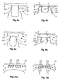
- the 10a, b shows a contact arrangement with a first contact piece 1 and a second contact piece 2.
- the first contact piece 1 has flexible contact segment 11, which a plurality side by side arranged flexible contact finger 111.112 comprises.
- the in Fig. 10a, b The six contact fingers 111, 112 shown are (in half) in two groups divided three contact fingers 111 or 112, preferably are arranged essentially mirror images. But 2, 3, 4, 5, 7, 8, 9, 10 or more, for example 12, 14, 16 or 18 contact fingers 111,112 are shown.
- the contact fingers 111, 112 are elongated trained and walking stick-shaped or in the manner of a curved finger bent.
- the ratio of length to wall thickness of the contact fingers 111, 112 is advantageously in the range from 5: 1 1 to 100: 1, particularly advantageously in the range from 12: 1 to 40: 1 or advantageously also in the range from 20: 1 to 30: 1. These length-to-wall thickness ratios are also for that other contact fingers shown in this description (see Figs. 7, 8, 9, 12). At one end are the contact fingers 111, 112 with the contact segment carrier 12 connected. At its other end (according to the handle of the walking stick or the tip of the finger) they are free. The direction of the Curvature of the contact fingers 111 (at their free end) is advantageous Curvature of the contact fingers 112 opposite. 10a is the first Switching status A (open) shown.
- each contact finger 111, 112 is advantageously chosen such that an envelope of its free Ends essentially of the surface facing the contact fingers 111, 112 of the second contact piece 2 corresponds. At least that has Envelope in the second switching state (FIG. 10b) advantageously has such a shape, so that the contact fingers 111, 112 then contact the second contact piece 2 nestle.
- the first contact piece 1 and the second contact piece 2 a plurality of contact points 5 on. It can also be a plurality of contact areas 5.
- the individual contact fingers 111, 112 of the flexible contact segment 11 are elastically deformed by the second contact piece 2.
- the flexible contact segment 11 is formed on the second contact piece 2.
- the contact fingers 111, 112 of the flexible contact segment move 11 sliding against the second contact piece 2, so that the self-cleaning effect mentioned above occurs.
- a contact arrangement according to Fig. 10a, b has the advantage that a minimum number of contact points 5 or contact areas 5 can be predetermined, so that a safe contact with low contact resistance can always be achieved is.
- FIG. 11a, b illustrate a further advantageous embodiment.
- Fig. 11a shows the first switching state A
- Fig. 11b the second Switching state B.
- the contact arrangement has three contact pieces 1, 2, 3.
- the first contact piece 1 comprises a flexible contact segment 11 and one Contact segment carrier 12.
- the third contact piece 3 comprises a flexible Contact segment 31 and a contact segment carrier 32.
- the third Contact piece 3 is preferably mirror-symmetrical to the first contact piece 1 trained and arranged.
- the second contact piece 2 comprises one rigid section and one connected to the rigid section Contact carrier 22.
- the second contact piece 2 is the driven contact piece.
- the direction of the relative movement of the second contact piece 2 opposite the contact pieces 2 and 3 is shown by a dashed line.
- the rigid section of the second contact piece 2 has two essentially flat surfaces with the direction of the relative movement of the second Contact piece 2 relative to the contact pieces 1 and 3 an angle ⁇ ' lock in.
- the second switching state B Fig. 11b
- These touch surfaces 5 in the second switching state B close with the direction of the relative Movement of the second contact piece 2 relative to the contact pieces 1 and 3 an angle ⁇ .
- This angle ⁇ is preferably in the range of about 45 ° ⁇ 30 °, especially in the range of 45 ° ⁇ 15 °. Because of the rigidity of the rigid section of the second contact piece 2 becomes the rigid section essentially not elastically deformed during switching operations. Therefore the angles ⁇ and ⁇ 'are essentially the same.
- a contact arrangement is shown, which is similar to that in Fig. 7a, b is shown. It is described on the basis of this.
- second contact piece 2 has a clear taper, in particular a waist on.
- the contact fingers 111, 112 of the flexible contact segment 11 are clear S-shaped, so that the contact segment carrier 12 further away bellies of the two "S" in the second switching state B (Fig. 12b) engage in the mentioned taper.
- the one to turn on (A to B) introductory energy to be applied and also to the Execution energy to be applied (B to A) is large.
- the Execution energy is so great that a monostable switchable contact segment carrier 12, like that shown in Fig.
- the first stable position is the natural, manufacturing-related stable position of the monostable bendable contact segment carrier 12 (Fig. 12a, switching state A).
- the second stable position (Fig. 12b, second switching state) is the inherently unstable, bent position of the bendable contact segment carrier 12, in which the contact arrangement however, the execution energy remains until appropriately is applied. Due to the flexible contact segment 11 Contact arrangement thus held in the second stable switching position B.
- the push button principle By means of the push button principle, a bistable switchable contact arrangement is created realized.
- the number of stable positions for the contact segment carrier can be increased by at least one.
- a not shown An example of a two stable position increase is one at one end clamped beam, which is flexible at its free end on each side
- Contact segments of the type of the flexible contact segment shown in Fig. 12a, b has, each of these flexible contact segments with one each another contact piece cooperates in the manner of the push button principle. This results in three stable positions of the contact segment carrier instead of just one.
- this improves, safer Contact arrangements created that due to its thin walls flexible contact segment 11 during a switching operation by means of mostly rigid second contact segment 2 is elastically deformed.
- the flexible contact segment 11 is different from the drive 4 and is not directly deformed by the drive 4.
- the flexible contact segment both when switching from the first in the second also when switching from elastically deform the second to the first switching state. It is also conceivable that one of these (re) deformations only (shortly) after the switching process (and before another switching operation) takes place, such (Re) deformation can also be induced, i.e. not by itself, but stimulated, for example by electrostatic forces.
- the contact arrangements can be made using one or more structuring methods, such as DRIE, 3D UV depth lithography, LIGA technology or other structuring processes from semiconductor manufacturing (Coating, etching).
- structuring methods such as DRIE, 3D UV depth lithography, LIGA technology or other structuring processes from semiconductor manufacturing (Coating, etching).
- Silicon carbide is particularly suitable (SiC), germanium (Ge), gallium arsenide (GaAs), gallium nitride (GaN), InSb (indium antimonide), InP (indium phosphide), quartz and diamond.
- SiC silicon carbide
- germanium Ge
- gallium arsenide GaAs
- GaN gallium nitride
- InSb indium antimonide
- InP indium phosphide
- quartz and diamond One is important high tensile strength, high abrasion resistance and low mechanical Fatigue.
- Materials with a tensile strength of at least 40 N / m 2 , more preferably at least 50 N / m 2 or even better at least 60 N / m 2 are preferably used.
- Silicon has a tensile strength of 69 N / m 2
- steel typically has 21 N / m 2 , maximum 42 N / m 2 .
- coatings can also be applied to the contact pieces, in particular to the flexible contact segment.
- Carbides, nitrides and oxides are particularly suitable for this.
- SiC has a tensile strength of 210 N / m 2 , Si 3 N 4 one of 140 N / m 2 and SiO 2 one of 84 N / m 2 .
- Hardness is an important factor in terms of abrasion resistance.
- Silicon has a Knoop hardness of 850 kg / mm 2
- stainless steel has 660 kg / mm 2
- tungsten 400 kg / mm 2 and aluminum only 130 kg / mm 2 .
- Coatings can also be advantageous for achieving improved abrasion resistance, for example with SiC (Knoop hardness 2480 kg / mm 2 ) or Si 3 N 4 (3486 kg / mm 2 ).
- the contact arrangement switches electrical currents metallic coatings to reduce contact resistance (electrical, but also thermally) is an advantage.
- the contact pieces 1,2 then point metallic surfaces, which in the second switching state B touch.
- Semiconducting materials are advantageously doped, so that they are a have good electrical conductivity.
- Monocrystalline silicon is extremely small due to its manufacture Defect density.
- the generation of smooth surfaces with single-crystal Silicon is simple. So one can, with ordinary metals like compared to polycrystalline steel or aluminum, extremely low material fatigue be achieved.
- the contact arrangements can advantageously be two, three, four, five, six or include more contact pieces.
- One, two or more of them can be driven or be agile.
- One, two or more each have one or several flexible contact segments 11, which are driven (movable) or non-driven (non-movable) contact pieces can act, and wherein one or more driven (movable) while one or more others are not driven (not movable).
- a first one provided with a flexible contact segment Contact piece and a second, essentially non-deformable Contact piece can also such a second contact piece can be used, which is a flexible contact segment or has an elastically deformable section.
- the contact pieces with a flexible contact segment each formed in one piece.
- a contact arrangement according to the invention can also have several first switching states A and / or have a plurality of second switching states B.
- first switching states A and / or have a plurality of second switching states B.
- second switching states B for example in the case of a two-way switching relay with one open and two closed States, see for example also the unpublished mentioned European patent application with the file number 02405334.0.
- the drive 4 and any other drives 4 can be electrostatic, for example, but also electromagnetic, piezoelectric or thermal work.
- the contact arrangement or the MEMS can be one act lateral structure, in which movements essentially parallel to the substrate (horizontal) run. But it can also be a vertical structure be in which movements are substantially perpendicular to the substrate.
- the contact arrangements can advantageously be used in switching devices, which are able to generate a high contact pressure, as is the case for example the case with the bendable contact segment carriers mentioned is.
- Switches and micro-relays with one according to the invention can advantageously be used Contact arrangement can be equipped.
- Switches can advantageously automated test devices (ATE, automated test equipment).
- ATE automated test devices
Landscapes
- Physics & Mathematics (AREA)
- Electromagnetism (AREA)
- Push-Button Switches (AREA)
- Slide Switches (AREA)
- Relay Circuits (AREA)
- Interface Circuits In Exchanges (AREA)
Abstract
Description
- Fig. 1
- ein erfindungsgemässes MEMS-Relais mit membranförmigem flexiblen Kontaktsegment und elektrostatischen Antrieben;
- Fig.2a
- eine erfindungsgemässe MEMS-Kontaktanordnung mit zwei Kontaktstücken und mit membranförmigem flexiblen Kontaktsegment, geöffnet;
- Fig. 2b
- wie Fig. 2a, geschlossen;
- Fig. 3a
- eine erfindungsgemässe MEMS-Kontaktanordnung mit drei Kontaktstücken, mit membranförmigem flexiblen Kontaktsegment, geöffnet;
- Fig. 3b
- wie Fig. 3a, geschlossen;
- Fig.4a
- eine erfindungsgemässe MEMS-Kontaktanordnung mit zwei Kontaktstücken und mit asymmetrischem membranförmigem flexiblen Kontaktsegment, geöffnet;
- Fig. 4b,4c
- wie Fig. 4a, geschlossen;
- Fig. 5
- eine erfindungsgemässe MEMS-Kontaktanordnung mit drei Kontaktstücken und mit membranförmigem flexiblen Kontaktsegment auf einer Basis, geöffnet;
- Fig. 6
- wie Fig. 5, zusätzlich noch mit Federmechanismus;
- Fig. 7a
- eine erfindungsgemässe MEMS-Kontaktanordnung mit zwei Kontaktstücken nach Art eines Stecker-Steckdosenpaares und mit zwei Kontaktfingern, geöffnet;
- Fig. 7b
- wie Fig. 7a, geschlossen;
- Fig. 8a
- eine erfindungsgemässe MEMS-Kontaktanordnung mit zwei Kontaktstücken nach Art eines Stecker-Steckdosenpaares und mit zwei Kontaktfingern, geöffnet;
- Fig. 8b
- wie Fig. 8a, geschlossen;
- Fig. 9a
- wie Fig. 8a, zusätzlich noch mit Basis;
- Fig. 9b
- wie Fig. 9a, geschlossen;
- Fig. 10a
- eine erfindungsgemässe MEMS-Kontaktanordnung mit zwei Kontaktstücken und mit einer Mehrzahl von spiegelsymmetrisch angeordneten Kontaktfingern, geöffnet;
- Fig. 10b
- wie Fig. 10a, geschlossen;
- Fig. 11a
- eine erfindungsgemässe MEMS-Kontaktanordnung mit drei Kontaktstücken und mit gewinkelten, reibungserzeugenden Berührungsflächen, geöffnet;
- Fig. 11b
- wie Fig. 11a, geschlossen;
- Fig. 12a
- ein erfindungsgemässes MEMS mit zwei Kontaktstücken, wobei mittels des Druckknopf-Prinzips eine bistabile Schaltbarkeit erreicht wird, geöffnet;
- Fig. 12b
- wie Fig. 12a, geschlossen;
- 1
- erstes Kontaktstück
- 11
- flexibles Kontaktsegment
- 1 11,112
- Kontaktfinger des flexiblen Kontaktsegments
- 113
- Basis des flexiblen Kontaktsegments
- 114
- Volumen
- 12
- Kontaktsegment-Träger
- 13
- Mittel zur Federung
- 2
- zweites Kontaktstück
- 22
- Kontakt-Träger des zweiten Kontaktstücks
- 3
- drittes Kontaktstück
- 31
- flexibles Kontaktsegment des dritten Kontaktstücks
- 32
- Kontaktsegment-Träger des dritten Kontaktstücks
- 4
- Antrieb
- 5,5'
- Berührungsbereich, Berührungsfläche, Berührungspunkt zwischen erstem Kontaktstück und zweitem Kontaktstück
- 6
- zusätzlicher Berührungspunkt im zweiten Schaltzustand zwischen flexiblem Kontaktsegment und Kontaktsegment-Träger oder Basis
- A
- erster Schaltzustand (geöffnet)
- B
- zweiter Schaltzustand (geschlossen)
- d
- Wanddicke (des flexiblen Abschnitts) des flexiblen Kontaktsegments
- α
- Winkel
- ε
- Winkel
Claims (17)
- MEMS-Kontaktanordnung, mit mindestens einem ersten Kontaktstück (1 ) und einem zweiten Kontaktstück (2), wobei mindestens eines der beiden Kontaktstücke (1 ;2) antreibbar ist, und wobei die MEMS-Kontaktanordnung mittels des antreibbaren Kontaktstücks (1;2) bei einem Schaltvorgang zwischen einem ersten Schaltzustand (A) und mindestens einem zweiten Schaltzustand (B) schaltbar ist, wobei die beiden Kontaktstücke (1,2) in dem ersten Schaltzustand (A) voneinander getrennt sind und in dem zweiten Schaltzustand (B) einander kontaktierend sind,
dadurch gekennzeichnet, dass mindestens das erste Kontaktstück (1) mindestens ein flexibles Kontaktsegment (11) und einen Kontaktsegment-Träger (12) aufweist, und
dass das mindestens eine flexible Kontaktsegment (11 ) mittels mindestens des zweiten Kontaktstücks (2) bei dem Schaltvorgang elastisch verformbar ist. - MEMS-Kontaktanordnung gemäss Anspruch 1, dadurch gekennzeichnet, dass das mindestens eine flexible Kontaktsegment (11 ) mittels mindestens des zweiten Kontaktstücks (2) bei einem Schaltvorgang von dem ersten Schaltzustand (A) in den zweiten Schaltzustand (B) elastisch derart verformbar ist, dass das mindestens eine flexible Kontaktsegment (1 1 ) mit dem zweiten Kontaktstück (2) in dem zweiten Schaltzustand (B) mindestens einen flächigen Berührungsbereich (5) oder eine vorgebbare Mehrzahl von Berührungspunkten (5,5') aufweist.
- MEMS-Kontaktanordnung gemäss einem der vorangehenden Ansprüche,
dadurch gekennzeichnet, dass im ersten Schaltzustand (A) die Form des flexiblen Kontaktsegments (11) verschieden ist von der Form des flexiblen Kontaktsegments (11) im zweiten Schaltzustand (B), und
dass im zweiten Schaltzustand (B) das flexible Kontaktsegment (11) dem zweiten Kontaktstück (2) angeformt ist. - MEMS-Kontaktanordnung gemäss einem der vorangehenden Ansprüche,
dadurch gekennzeichnet, dass im ersten Schaltzustand (A) die Form des flexiblen Kontaktsegments (11) verschieden ist von der Form des flexiblen Kontaktsegments (11) im zweiten Schaltzustand (B),
dass das mindestens eine flexible Kontaktsegment (11) mit dem zweiten Kontaktstück (2) in dem zweiten Schaltzustand (B) mindestens einen flächigen Berührungsbereich (5) aufweist,
dass im zweiten Schaltzustand (B) das flexible Kontaktsegment (11) in dem Berührungsbereich (5) dem zweiten Kontaktstück (2) angeformt ist, und
dass im zweiten Schaltzustand (B) das zweite Kontaktstück (2) in dem Berührungsbereich (5) von dem ersten Kontaktstück (1) flächig umschlossen ist. - MEMS-Kontaktanordnung gemäss einem der vorangehenden Ansprüche,
dadurch gekennzeichnet, dass bei dem Schaltvorgang das zweite Kontaktstück (2) gegenüber dem flexiblen Kontaktsegment (11) gleitreibend beweglich ist. - MEMS-Kontaktanordnung gemäss einem der vorangehenden Ansprüche,
dadurch gekennzeichnet, dass das flexible Kontaktsegment (11) aufgrund seiner Dünnwandigkeit flexibel und elastisch verformbar ist,
insbesondere dass das flexible Kontaktsegment (11) einen flexiblen Abschnitt mit einer Wanddicke zwischen 1 µm und 60 µm, vorzugsweise mit einer Wanddicke zwischen 5 µm und 25 µm, aufweist, und
insbesondere dass die elastischen Verformungen mindestens von der Grössenordnung der Wanddicke des flexiblen Abschnitts des flexiblen Kontaktsegments (11) sind und/oder im Bereich des 0.5- bis 20-fachen, insbesondere des 1- bis 5-fachen der Wanddicke eines flexiblen Abschnitts des flexiblen Kontaktsegments (11) liegen. - MEMS-Kontaktanordnung gemäss einem der vorangehenden Ansprüche,
dadurch gekennzeichnet, dass das erste Kontaktstück (1) einstückig ausgebildet ist. - MEMS-Kontaktanordnung gemäss einem der vorangehenden Ansprüche,
dadurch gekennzeichnet, dass das flexible Kontaktsegment (11) zusätzlich zu mindestens einem flexiblen Abschnitt noch eine dem Kontaktsegment-Träger (12) zugewandte Basis (113) beinhaltet, welche Basis (113) eine grössere Wanddicke aufweist als der mindestens eine flexible Abschnitt. - MEMS-Kontaktanordnung gemäss einem der vorangehenden Ansprüche,
dadurch gekennzeichnet, dass zur elastischen Verformung des mindestens einen flexiblen Kontaktsegments (11) mittels mindestens des zweiten Kontaktstücks (2) bei einem Schaltvorgang von dem ersten Schaltzustand (A) in den zweiten Schaltzustand (B) eine Einführungsenergie aufzubringen ist,
dass zur elastischen Verformung des mindestens einen flexiblen Kontaktsegments (11) mittels mindestens des zweiten Kontaktstücks (2) bei einem Schaltvorgang von dem zweiten Schaltzustand (B) in den ersten Schaltzustand (A) eine Ausführungsenergie aufzubringen ist, und
dass im zweiten Schaltzustand (B) von dem flexiblen Kontaktsegment (11) auf das zweite Kontaktstück (2) eine Rückhaltekraft ausübbar ist, durch welche Rückhaltekraft ein Schaltvorgang von dem zweiten Schaltzustand (B) in den ersten Schaltzustand (A) erschwert ist. - MEMS-Kontaktanordnung gemäss einem der vorangehenden Ansprüche,
dadurch gekennzeichnet, dass der Kontaktsegment-Träger (12) ein Schaltelement mit mindestens einer stabilen Position ist, und
dass das flexible Kontaktsegment (11) und das zweite Kontaktstück (2) nach Art des Druckknopf-Prinzips derart zusammenwirken, dass der Kontaktsegment-Träger (12) mindestens eine weitere stabile Position aufweist. - MEMS-Kontaktanordnung gemäss einem der vorangehenden Ansprüche,
dadurch gekennzeichnet, dass das flexible Kontaktsegment (11) und das zweite Kontaktstück (2) nach Art eines Stecker-Steckdosen-Paares ineinanderfügbar sind. - MEMS-Kontaktanordnung gemäss einem der vorangehenden Ansprüche,
dadurch gekennzeichnet, dass das flexible Kontaktsegment (11) eine Mehrzahl von elastisch verformbaren Kontaktfingern (111, 112) aufweist. - MEMS-Kontaktanordnung gemäss einem der vorangehenden Ansprüche,
dadurch gekennzeichnet, dass das mindestens eine flexible Kontaktsegment (11) in dem zweiten Schaltzustand (B) mindestens einen flächigen Berührungsbereich (5) mit dem zweiten Kontaktstück (2) aufweist,
dass die Richtung der Relativbewegung von dem flexiblen Kontaktsegment (11) und dem zweiten Kontaktstück (2) bei dem Schaltvorgang mit dem flächigen Berührungsbereich (5) im wesentlichen einen Winkel α = 45° ± 30°, insbesondere α = 45° ± 15°, einschliesst, und
dass diejenigen Flächen des flexiblen Kontaktsegments (11) und des zweiten Kontaktstücks (2), die im zweiten Schaltzustand (B) im wesentlichen parallel zueinander ausgerichtet sind und einander in dem flächigen Berührungsbereich (5) berühren, im ersten Schaltzustand (A) im wesentlichen bis auf einen Winkel ε mit 0° ≤ ε ≤ 30°, insbesondere 0° ≤ ε ≤ 10°, parallel zueinander ausgerichtet sind. - MEMS-Kontaktanordnung gemäss einem der vorangehenden Ansprüche,
dadurch gekennzeichnet, dass das flexible Kontaktsegment (11) einen membranartigen Abschnitt beinhaltet, der bei dem Schaltvorgang elastisch verformbar ist. - MEMS-Kontaktanordnung gemäss einem der vorangehenden Ansprüche,
dadurch gekennzeichnet, dass von dem flexiblen Kontaktsegment (11) oder von dem flexiblen Kontaktsegment (11) gemeinsam mit dem ersten Kontaktstück (1) ein Volumen (114) umschlossen wird, welches im wesentlichen mit einer elektrisch und thermisch leitfähigen, elastisch verformbaren Füllung gefüllt ist. - MEMS-Schaltgerät dadurch gekennzeichnet, dass das MEMS-Schaltgerät eine MEMS-Kontaktanordnung gemäss einem der vorangehenden Ansprüche beinhaltet.
- MEMS-Schaltgerät gemäss Anspruch 16, dadurch gekennzeichnet, dass das MEMS-Schaltgerät ein Mikro-Relais mit einem Antrieb (4) ist, und insbesondere dass der Antrieb (4) ein elektrostatischer Antrieb (4) ist.
Priority Applications (3)
| Application Number | Priority Date | Filing Date | Title |
|---|---|---|---|
| AT02405741T ATE349762T1 (de) | 2002-08-30 | 2002-08-30 | Mems-kontaktanordnung und mikro-relais |
| EP02405741A EP1394825B1 (de) | 2002-08-30 | 2002-08-30 | MEMS-Kontaktanordnung und Mikro-Relais |
| DE50209085T DE50209085D1 (de) | 2002-08-30 | 2002-08-30 | MEMS-Kontaktanordnung und Mikro-Relais |
Applications Claiming Priority (1)
| Application Number | Priority Date | Filing Date | Title |
|---|---|---|---|
| EP02405741A EP1394825B1 (de) | 2002-08-30 | 2002-08-30 | MEMS-Kontaktanordnung und Mikro-Relais |
Publications (2)
| Publication Number | Publication Date |
|---|---|
| EP1394825A1 true EP1394825A1 (de) | 2004-03-03 |
| EP1394825B1 EP1394825B1 (de) | 2006-12-27 |
Family
ID=31198013
Family Applications (1)
| Application Number | Title | Priority Date | Filing Date |
|---|---|---|---|
| EP02405741A Expired - Lifetime EP1394825B1 (de) | 2002-08-30 | 2002-08-30 | MEMS-Kontaktanordnung und Mikro-Relais |
Country Status (3)
| Country | Link |
|---|---|
| EP (1) | EP1394825B1 (de) |
| AT (1) | ATE349762T1 (de) |
| DE (1) | DE50209085D1 (de) |
Cited By (2)
| Publication number | Priority date | Publication date | Assignee | Title |
|---|---|---|---|---|
| DE102006043512A1 (de) * | 2006-05-22 | 2007-11-29 | Continental Teves Ag & Co. Ohg | Beschleunigungsschalter |
| WO2023135083A1 (de) * | 2022-01-13 | 2023-07-20 | Robert Bosch Gmbh | Kontaktelement eines mems-relais |
Citations (4)
| Publication number | Priority date | Publication date | Assignee | Title |
|---|---|---|---|---|
| US6020564A (en) * | 1998-06-04 | 2000-02-01 | Wang Electro-Opto Corporation | Low-voltage long life electrostatic microelectromechanical system switches for radio-frequency applications |
| DE19950964A1 (de) * | 1998-10-23 | 2000-05-18 | Fraunhofer Ges Forschung | Mikromechanisches Relais und Verfahren zur Herstellung |
| WO2002039472A1 (en) * | 2000-11-09 | 2002-05-16 | Raytheon Company | Micro-relay contact structure for rf applications |
| WO2002058089A1 (en) * | 2001-01-19 | 2002-07-25 | Massachusetts Institute Of Technology | Bistable actuation techniques, mechanisms, and applications |
-
2002
- 2002-08-30 AT AT02405741T patent/ATE349762T1/de not_active IP Right Cessation
- 2002-08-30 EP EP02405741A patent/EP1394825B1/de not_active Expired - Lifetime
- 2002-08-30 DE DE50209085T patent/DE50209085D1/de not_active Expired - Lifetime
Patent Citations (4)
| Publication number | Priority date | Publication date | Assignee | Title |
|---|---|---|---|---|
| US6020564A (en) * | 1998-06-04 | 2000-02-01 | Wang Electro-Opto Corporation | Low-voltage long life electrostatic microelectromechanical system switches for radio-frequency applications |
| DE19950964A1 (de) * | 1998-10-23 | 2000-05-18 | Fraunhofer Ges Forschung | Mikromechanisches Relais und Verfahren zur Herstellung |
| WO2002039472A1 (en) * | 2000-11-09 | 2002-05-16 | Raytheon Company | Micro-relay contact structure for rf applications |
| WO2002058089A1 (en) * | 2001-01-19 | 2002-07-25 | Massachusetts Institute Of Technology | Bistable actuation techniques, mechanisms, and applications |
Cited By (2)
| Publication number | Priority date | Publication date | Assignee | Title |
|---|---|---|---|---|
| DE102006043512A1 (de) * | 2006-05-22 | 2007-11-29 | Continental Teves Ag & Co. Ohg | Beschleunigungsschalter |
| WO2023135083A1 (de) * | 2022-01-13 | 2023-07-20 | Robert Bosch Gmbh | Kontaktelement eines mems-relais |
Also Published As
| Publication number | Publication date |
|---|---|
| DE50209085D1 (de) | 2007-02-08 |
| ATE349762T1 (de) | 2007-01-15 |
| EP1394825B1 (de) | 2006-12-27 |
Similar Documents
| Publication | Publication Date | Title |
|---|---|---|
| DE4437261C1 (de) | Mikromechanisches elektrostatisches Relais | |
| DE60105899T2 (de) | Schaltvorrichtung, insbesondere zum optischen schalten | |
| EP0938738B1 (de) | Verfahren zum herstellen eines mikromechanischen relais | |
| EP0685109A1 (de) | Mikromechanisches relais mit hybridantrieb. | |
| DE10302618B4 (de) | Elektrostatische Betätigungsvorrichtung | |
| DE19823690C1 (de) | Mikromechanisches elektrostatisches Relais | |
| EP1163692B1 (de) | Substratparallel arbeitendes mikrorelais | |
| DE102021202409A1 (de) | Kapazitiv betätigbarer MEMS-Schalter | |
| DE602004008648T2 (de) | Bistabiler mikromechanischer schalter, betätigungsverfahren und entsprechendes verfahren zu seiner realisierung | |
| DE3135652A1 (de) | Schalter mit gleitendem ueberbrueckungskontaktgeber | |
| EP1468436B1 (de) | Mikro-elektromechanisches system und verfahren zu dessen herstellung | |
| EP1394825A1 (de) | MEMS-Kontaktanordnung und Mikro-Relais | |
| EP3105770B1 (de) | Mikro-elektro-mechanisches system und verfahren zum herstellen desselben | |
| DE3421021C2 (de) | ||
| EP1246215B1 (de) | Mikrorelais mit neuem Aufbau | |
| DE10015598A1 (de) | Mikroaktoranordnung | |
| DE4113190C1 (en) | Electrostatically actuated microswitch - has armature attached to base via torsional struts to allow pivoting for contacting electrodes | |
| CH450521A (de) | Kippwerk, insbesondere für eine Schaltvorrichtung | |
| DE1960733A1 (de) | Elektrischer Schalter | |
| EP4584814A1 (de) | Transferstempel und verfahren zum erzeugen eines transferstempels | |
| DE3421806C2 (de) | ||
| DE60217802T2 (de) | Durch niedrige Spannung gesteuertes Mikroschaltbauelement | |
| EP1312100B1 (de) | Mikroschalter | |
| DE588517C (de) | Kipphebelschalter | |
| DE19950964A1 (de) | Mikromechanisches Relais und Verfahren zur Herstellung |
Legal Events
| Date | Code | Title | Description |
|---|---|---|---|
| PUAI | Public reference made under article 153(3) epc to a published international application that has entered the european phase |
Free format text: ORIGINAL CODE: 0009012 |
|
| AK | Designated contracting states |
Kind code of ref document: A1 Designated state(s): AT BE BG CH CY CZ DE DK EE ES FI FR GB GR IE IT LI LU MC NL PT SE SK TR |
|
| AX | Request for extension of the european patent |
Extension state: AL LT LV MK RO SI |
|
| 17P | Request for examination filed |
Effective date: 20040830 |
|
| AKX | Designation fees paid |
Designated state(s): AT BE BG CH CY CZ DE DK EE ES FI FR GB GR IE IT LI LU MC NL PT SE SK TR |
|
| 17Q | First examination report despatched |
Effective date: 20041213 |
|
| GRAP | Despatch of communication of intention to grant a patent |
Free format text: ORIGINAL CODE: EPIDOSNIGR1 |
|
| GRAS | Grant fee paid |
Free format text: ORIGINAL CODE: EPIDOSNIGR3 |
|
| GRAA | (expected) grant |
Free format text: ORIGINAL CODE: 0009210 |
|
| AK | Designated contracting states |
Kind code of ref document: B1 Designated state(s): AT BE BG CH CY CZ DE DK EE ES FI FR GB GR IE IT LI LU MC NL PT SE SK TR |
|
| PG25 | Lapsed in a contracting state [announced via postgrant information from national office to epo] |
Ref country code: CZ Free format text: LAPSE BECAUSE OF FAILURE TO SUBMIT A TRANSLATION OF THE DESCRIPTION OR TO PAY THE FEE WITHIN THE PRESCRIBED TIME-LIMIT Effective date: 20061227 Ref country code: IE Free format text: LAPSE BECAUSE OF FAILURE TO SUBMIT A TRANSLATION OF THE DESCRIPTION OR TO PAY THE FEE WITHIN THE PRESCRIBED TIME-LIMIT Effective date: 20061227 Ref country code: DK Free format text: LAPSE BECAUSE OF FAILURE TO SUBMIT A TRANSLATION OF THE DESCRIPTION OR TO PAY THE FEE WITHIN THE PRESCRIBED TIME-LIMIT Effective date: 20061227 Ref country code: FI Free format text: LAPSE BECAUSE OF FAILURE TO SUBMIT A TRANSLATION OF THE DESCRIPTION OR TO PAY THE FEE WITHIN THE PRESCRIBED TIME-LIMIT Effective date: 20061227 Ref country code: SK Free format text: LAPSE BECAUSE OF FAILURE TO SUBMIT A TRANSLATION OF THE DESCRIPTION OR TO PAY THE FEE WITHIN THE PRESCRIBED TIME-LIMIT Effective date: 20061227 Ref country code: NL Free format text: LAPSE BECAUSE OF FAILURE TO SUBMIT A TRANSLATION OF THE DESCRIPTION OR TO PAY THE FEE WITHIN THE PRESCRIBED TIME-LIMIT Effective date: 20061227 |
|
| REG | Reference to a national code |
Ref country code: GB Ref legal event code: FG4D Free format text: NOT ENGLISH |
|
| REG | Reference to a national code |
Ref country code: IE Ref legal event code: FG4D Free format text: LANGUAGE OF EP DOCUMENT: GERMAN |
|
| REF | Corresponds to: |
Ref document number: 50209085 Country of ref document: DE Date of ref document: 20070208 Kind code of ref document: P |
|
| PG25 | Lapsed in a contracting state [announced via postgrant information from national office to epo] |
Ref country code: SE Free format text: LAPSE BECAUSE OF FAILURE TO SUBMIT A TRANSLATION OF THE DESCRIPTION OR TO PAY THE FEE WITHIN THE PRESCRIBED TIME-LIMIT Effective date: 20070327 Ref country code: BG Free format text: LAPSE BECAUSE OF FAILURE TO SUBMIT A TRANSLATION OF THE DESCRIPTION OR TO PAY THE FEE WITHIN THE PRESCRIBED TIME-LIMIT Effective date: 20070327 |
|
| PG25 | Lapsed in a contracting state [announced via postgrant information from national office to epo] |
Ref country code: ES Free format text: LAPSE BECAUSE OF FAILURE TO SUBMIT A TRANSLATION OF THE DESCRIPTION OR TO PAY THE FEE WITHIN THE PRESCRIBED TIME-LIMIT Effective date: 20070407 |
|
| PG25 | Lapsed in a contracting state [announced via postgrant information from national office to epo] |
Ref country code: PT Free format text: LAPSE BECAUSE OF FAILURE TO SUBMIT A TRANSLATION OF THE DESCRIPTION OR TO PAY THE FEE WITHIN THE PRESCRIBED TIME-LIMIT Effective date: 20070528 |
|
| NLV1 | Nl: lapsed or annulled due to failure to fulfill the requirements of art. 29p and 29m of the patents act | ||
| GBV | Gb: ep patent (uk) treated as always having been void in accordance with gb section 77(7)/1977 [no translation filed] |
Effective date: 20061227 |
|
| ET | Fr: translation filed | ||
| PLBE | No opposition filed within time limit |
Free format text: ORIGINAL CODE: 0009261 |
|
| STAA | Information on the status of an ep patent application or granted ep patent |
Free format text: STATUS: NO OPPOSITION FILED WITHIN TIME LIMIT |
|
| PG25 | Lapsed in a contracting state [announced via postgrant information from national office to epo] |
Ref country code: GB Free format text: LAPSE BECAUSE OF FAILURE TO SUBMIT A TRANSLATION OF THE DESCRIPTION OR TO PAY THE FEE WITHIN THE PRESCRIBED TIME-LIMIT Effective date: 20061227 |
|
| 26N | No opposition filed |
Effective date: 20070928 |
|
| BERE | Be: lapsed |
Owner name: ABB RESEARCH LTD. Effective date: 20070831 |
|
| REG | Reference to a national code |
Ref country code: CH Ref legal event code: PL |
|
| PG25 | Lapsed in a contracting state [announced via postgrant information from national office to epo] |
Ref country code: MC Free format text: LAPSE BECAUSE OF NON-PAYMENT OF DUE FEES Effective date: 20070831 Ref country code: LI Free format text: LAPSE BECAUSE OF NON-PAYMENT OF DUE FEES Effective date: 20070831 Ref country code: CH Free format text: LAPSE BECAUSE OF NON-PAYMENT OF DUE FEES Effective date: 20070831 Ref country code: GR Free format text: LAPSE BECAUSE OF FAILURE TO SUBMIT A TRANSLATION OF THE DESCRIPTION OR TO PAY THE FEE WITHIN THE PRESCRIBED TIME-LIMIT Effective date: 20070328 |
|
| PG25 | Lapsed in a contracting state [announced via postgrant information from national office to epo] |
Ref country code: BE Free format text: LAPSE BECAUSE OF NON-PAYMENT OF DUE FEES Effective date: 20070831 |
|
| PG25 | Lapsed in a contracting state [announced via postgrant information from national office to epo] |
Ref country code: AT Free format text: LAPSE BECAUSE OF NON-PAYMENT OF DUE FEES Effective date: 20070830 |
|
| PG25 | Lapsed in a contracting state [announced via postgrant information from national office to epo] |
Ref country code: EE Free format text: LAPSE BECAUSE OF FAILURE TO SUBMIT A TRANSLATION OF THE DESCRIPTION OR TO PAY THE FEE WITHIN THE PRESCRIBED TIME-LIMIT Effective date: 20061227 |
|
| PG25 | Lapsed in a contracting state [announced via postgrant information from national office to epo] |
Ref country code: LU Free format text: LAPSE BECAUSE OF NON-PAYMENT OF DUE FEES Effective date: 20070830 Ref country code: CY Free format text: LAPSE BECAUSE OF FAILURE TO SUBMIT A TRANSLATION OF THE DESCRIPTION OR TO PAY THE FEE WITHIN THE PRESCRIBED TIME-LIMIT Effective date: 20061227 |
|
| PG25 | Lapsed in a contracting state [announced via postgrant information from national office to epo] |
Ref country code: TR Free format text: LAPSE BECAUSE OF FAILURE TO SUBMIT A TRANSLATION OF THE DESCRIPTION OR TO PAY THE FEE WITHIN THE PRESCRIBED TIME-LIMIT Effective date: 20061227 |
|
| PGFP | Annual fee paid to national office [announced via postgrant information from national office to epo] |
Ref country code: DE Payment date: 20100823 Year of fee payment: 9 Ref country code: FR Payment date: 20100901 Year of fee payment: 9 Ref country code: IT Payment date: 20100824 Year of fee payment: 9 |
|
| REG | Reference to a national code |
Ref country code: FR Ref legal event code: ST Effective date: 20120430 |
|
| PG25 | Lapsed in a contracting state [announced via postgrant information from national office to epo] |
Ref country code: IT Free format text: LAPSE BECAUSE OF NON-PAYMENT OF DUE FEES Effective date: 20110830 |
|
| REG | Reference to a national code |
Ref country code: DE Ref legal event code: R119 Ref document number: 50209085 Country of ref document: DE Effective date: 20120301 |
|
| PG25 | Lapsed in a contracting state [announced via postgrant information from national office to epo] |
Ref country code: FR Free format text: LAPSE BECAUSE OF NON-PAYMENT OF DUE FEES Effective date: 20110831 |
|
| PG25 | Lapsed in a contracting state [announced via postgrant information from national office to epo] |
Ref country code: DE Free format text: LAPSE BECAUSE OF NON-PAYMENT OF DUE FEES Effective date: 20120301 |