BACKGROUND OF THE INVENTION
1. Field of the Invention
The present invention relates to a copper foil
most suitable for a fine pattern circuit board,
especially for chip-on-film (COF) use or for a high-frequency
printed circuit board, and a copper foil most
suitable for an electromagnetic shield of a plasma
display panel (PDP). Further, the present invention
relates to a printed circuit board, a PDP electromagnetic
shield, and a high-frequency printed circuit board using
this copper foil.
2. Description of the Related Art
Along with the reduction in size and weight of
electronic devices, recent electronic parts have been
made highly integrated. Corresponding to this, the
circuit patterns of printed circuit boards also have had
to be made higher in density. Circuit patterns of a fine
line width and pitch are now being formed. In particular,
IC boards for driving the liquid crystal displays of
display units of personal computers, mobile phones, and
personal digital assistants (PDA) are being made
increasingly higher in density. As ICs are being directly
mounted on substrate films, these are called as "chip-on-film"
(COF) structures.
In COF mounting, the IC position is detected by
light passing through the film formed with the copper
foil interconnect patterns. However, the recognition rate
of a conventional electrodeposited copper foil for a
printed circuit board (ability to detect IC position by
light) is very poor. The reason is that the surface of
the copper foil is rough. That is, the parts of the film
through which the light penetrates are parts from which
unnecessary copper foil other than the copper circuit
parts are etched away. Unevenness of the surface of the
copper foil is transferred and remains on the surface of
the film when adhering the copper foil on the film. The
unevenness of the film surface therefore becomes larger.
Due to the unevenness, when the light passes, the amount
of the light able to proceed straight becomes smaller.
Therefore, the recognition rate becomes poor.
Conventional copper foil for printed circuit
boards is poor in this recognition rate. Therefore, a
two-layer material comprised of a polyimide film on which
copper layer is formed by sputtering (thin film
deposition process) and which is further copper plated is
used. However, this sputtered copper layer has only a
weak bonding strength to film. Therefore, there was the
possibility of the phenomenon that the etchant or plating
solution penetrates into the boundary between the copper
foil and the film, i.e., the "undercut phenomenon" during
the circuit manufacturing process. Further, due to the
weak bonding strength between sputtered copper layer and
the film, there is the danger of the copper foil peeling
off from the substrate during use as a product.
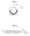
Ordinarily, electrodeposited copper foil
produced by an electrodeposited foil production apparatus
as shown in FIG. 1 is treated to prevent rust and to
roughen its surface to increase bondability by a surface
treatment apparatus as shown in FIG. 2. The
electrodeposited foil production apparatus comprises a
rotating drum-shaped cathode 2 (surface made of SUS or
titanium) and an anode 1 (lead or precious metal oxide
coated titanium electrode) arranged concentrically with
respect to the cathode 2. A current is passed across the
electrodes while circulating an electrolyte 3 to cause
the copper to deposit on the surface of the cathode 2 to
a predetermined thickness, then the copper is peeled off
from the surface of the cathode 2 as copper foil 4. In
the present specification, the copper foil at this stage
is called the "untreated copper foil 4", the surface of
the untreated copper foil 4 contacting the electrolyte 3
is called the "matt surface", and the surface contacting
the rotating drum shaped cathode 2 is called the "gloss
surface".
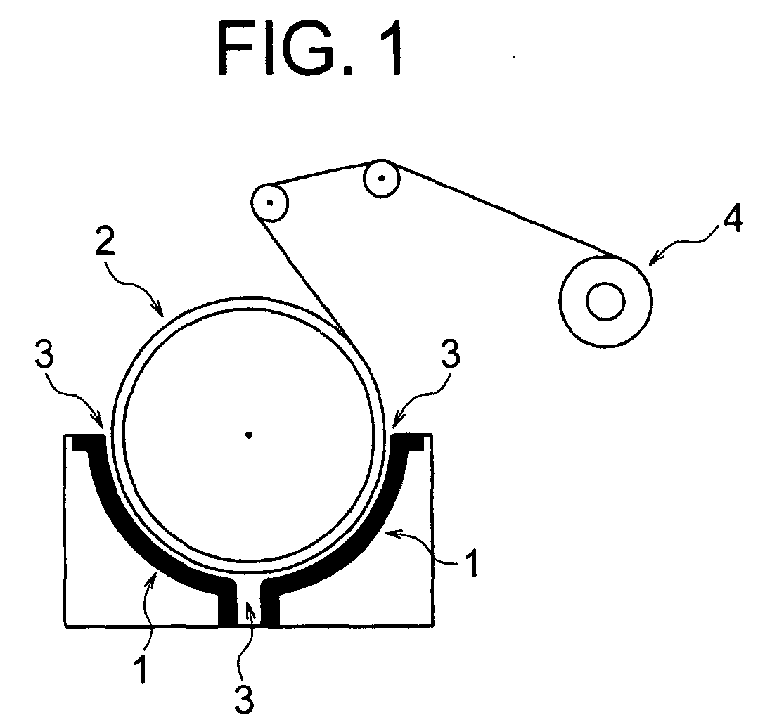
The untreated copper foil 4 is improved in
performance required for a printed circuit board, that is,
the bondability to a resin substrate, by being passed
through the surface treatment apparatus shown in FIG. 2
and subjected the continuous steps of electrochemical or
chemical surface treatment, that is, roughening, metal
plating, stainproofing, and silane coupling treatment. In
these surface treatments, the roughening is ordinarily
applied to the matt surface of the untreated copper foil.
The resultant copper foil is used as a surface treated
copper foil 8 for a printed circuit board. Note that, in
FIG. 2, reference numerals 5 and 6 indicate the
electrolyte and reference numeral 7 indicates an anode of
the surface treatment apparatus.
One of major factors influencing the etching
rate and recognition rate of the surface treated copper
foil 8 is the roughness of the copper foil surface. For
the etching rate, it is important that the roughness of
the matt surface and the gloss surface of the copper foil
both be small. For the recognition rate, it is important
that the surface roughness of the side to be bonded to
the film be small. Further, copper foil to be used for a
PDP electromagnetic shield is also required to be a
copper foil having a small surface roughness. A PDP is a
display panel using emission of light by electrodischarge
and is comprised of a glass vessel evacuated and then
filled with mercury gas etc. Voltage is applied to cause
electrodischarge. The ultraviolet light generated at this
time strikes fluorescent coating previously applied to
the inside of the glass vessel to cause emission of
visible light. PDP has mainly been used for display
applications at train stations and public facilities or
exhibitions and family restaurants, but recently demand
for household use large-scale televisions has been
increasing.
In a PDP, leakage of the electromagnetic waves
generated from the device is prevented by the arrangement
of an electromagnetic shield at the front of the display
(side close to viewer). As an electromagnetic shield for
electromagnetic waves leaking from devices used in public
facilities, use has been made of a sheet of glass
provided on its entire surface with a thin film of silver,
a fine nylon mesh material plated by copper, etc. However,
in a home television, further reduction of the
electromagnetic waves generated is required. This has
become difficult with a conventional shield. Therefore, a
type of shield comprised of a transparent film such as a
polyester film on which copper foil is bonded and etched
to leave a mesh of copper on the film has come into use.
This shield is arranged in front of the display. The
viewer views the light passing through parts without the
mesh copper. To obtain a good image quality, the mesh has
to have a good light transmission. Shields having a
copper foil mesh of a width of 10 µm and a pitch of 200
µm are now being mass produced.
Since this mesh is produced by etching, the
requirements on the copper foil for a PDP are similar to
the requirements on copper foil for a high density
printed circuit board. That is, in order to produce a
copper foil mesh having a fine width, it is necessary
that the roughness of the matt surface and the gloss
surface of the copper foil both be small. A copper foil
having a small surface roughness is required. Further,
electronic devices are not only being reduce in size and
weight, but also are being designed for further higher
frequencies along with the increase of information
transfer. Up to now, a high frequency signal over 1 GHz
had been used for restricted radio use such as
communications for aircraft and satellite communications,
but recently is being used also for familiar electronic
devices such as mobile phones and wireless LAN. The
printed circuit boards for such high frequencies have to
use a resin superior in high frequency characteristic.
The copper foil has to be one having less high-frequency
transfer loss. That is, the higher the frequency, the
more noticeable the "skin effect" where a signal passes
primarily at the surface part of a conductive layer. Due
to this, when using a conventional copper foil having a
large unevenness, the high-frequency transfer loss is
large. Therefore, it can no longer be used for such
applications.
A major factor influencing the high-frequency
transfer loss is the surface roughness. The higher the
frequency, the more noticeable the skin effect, so the
roughness of the matt surface and the gloss surface of
the copper foil both have to be small for the high-frequency
transfer loss. There are two major factors
influencing the roughness of the matt surface of the
copper foil. One is the surface roughness of the matt
surface of the untreated copper foil. Another is the
method of deposition of granular copper in the roughening.
If the surface roughness of the matt surface of the
untreated copper foil is large, the surface roughness of
the copper foil after roughening becomes large. The
amount of deposition of the granular copper in the
roughening can be adjusted by the current in the
roughening. But the surface roughness of the untreated
copper foil is primarily decided by the electrodeposition
conditions when the copper to be deposited on the above
drum-shaped cathode 2 in FIG. 1 and by the additives
added to the electrolyte 3.
General electrodeposited copper foil is
roughened on its matt surface to a surface roughness of
about 6 µm at a thickness of 12 µm and about 10 µm at a
thicker copper foil of 70 µm in terms of the surface
roughness Rz (Rz as defined in JIS B0601-1994,
"Definition and Description of Surface Roughness", 5.1
"Definition of 10-Point Average Roughness"). When the
copper foil bonding surface for bonding with the resin
substrate has a relatively large surface roughness in
this way, a high bonding strength where copper particles
which had been present on the roughened surface of the
copper foil and part of the copper foil deposited in a
branch-like manner deeply penetrate the resin substrate
is obtained. On the other hand, it takes time to dissolve
the copper particles and deposited copper in a branch-like
manner penetrating the resin substrate completely in
etching to form printed circuits resulting in the
occurrence of so-called "etching residue". As a result,
the bottom lines between the copper foil and the resin
substrate become poor in linearity and insulation between
adjacent circuits becomes poor when the distance between
circuits is made narrower. In notable cases, a circuit is
unable to be fabricated completely and the phenomenon of
bridging of adjacent circuits occurs.
Further, the gloss surface (surface of side
contacting drum) has gloss at first glance and seems to
be smooth, but becomes a replica of the drum surface. The
roughness is usually about 1.5 to 2.0 µm in terms of Rz
in average. This is because manufacture is started in a
state with the initial drum surface polished smooth, but
later the drum surface is dissolved and gradually becomes
rough along with continuance of manufacture of the
electrodeposited copper foil due to the electrolyte being
strongly acidic. If after manufacture of the
electrodeposited copper foil for a certain time the drum
surface becomes rough, the drum surface is polished again
to smooth it, but seen on an average, the roughness is
about 1.5 to 2.0 µm.
If the surface roughness is large, the
bondability of the dry film etching resist bonded to the
copper foil surface becomes locally good and locally bad.
Therefore, the circuit is sometimes formed in a wave
shape during etching. If becoming wavy in this way, the
circuit becomes poor in linearity and the problem arises
that it becomes difficult to form fine patterns. Further,
in a case of using a liquid resist, while the degree is
slight compared with a dry film resist, due to the
difference of the dissolution rate between depressions
and projections of the copper foil, the phenomenon of the
shape of the circuit becoming wavy is seen in the same
way. To deal with the requirement of increasing the
pattern fineness, in addition to the roughness of the
matt surface of the copper foil being small, it is
important that the roughness of the gloss surface also be
small.
Due to the above reasons, it is important that
the surface of the copper foil be small in surface
roughness of the side to be bonded with the film for the
recognition rate and it is important that the surface
roughness be small at both sides for a copper foil for
use in a plasma display panel and high-frequency printed
circuit board. Above, the importance of surface roughness
was described with reference to an electrodeposited
copper foil, but a rolled copper foil also has the same
problems of course.
SUMMARY OF THE INVENTION
An object of the present invention is to provide a
copper foil having a high etching factor, having superior
linearity of bottom lines of a circuit pattern, having no
copper partaicles remaining in the resin of the circuit
pattern, capable of forming fine pattern, superior in
recognition rate, and having a small high-frequency
transmission loss.
According to the present invention, there is
provided a copper foil for chip-on-film use, a plasma
display panel, or a high-frequency printed circuit board
obtained by rolling copper foil to smooth the surface to
give a surface area of not more than 1.30 times an ideal
smooth surface. The present invention is characterized by
rolling the copper foil (below, unless otherwise alluded
to, the term "copper foil" generally meaning an
electrodeposited copper foil and a rolled copper foil) to
smooth it to give a surface area as measured by a laser
microscope (made by KEYENCE Co., model number: VK-8510)
not more than 1.30 times, preferably not more than 1.20
times, of the ideal smooth surface.
Preferably, the smoothed copper foil surface is
plated by at least one metal of Ni and Zn. By smoothing
the copper foil surface by rolling and plating the smooth
surface of the copper foil by at least one metal of Ni
and Zn, it is possible to give bonding strength and
chemical resistance.
Alternatively, on the smoothed copper foil surface,
fine roughening particles of Cu or alloy particles of Cu
and Mo or alloy particles comprising Cu and at least one
element selected among a group of Ni, Co, Fe, and Cr or a
mixture of the alloy particles and an oxide of at least
one element selected among a group of V, Mo, and W are
deposited. By smoothing the copper foil surface by
rolling and making metal particles, alloy particles, or
mixtures of various particles to adhere as fine
roughening particles to the smoothed surface, fine
roughening particles are adhered to the smoothed surface
uniformly and the bonding strength with a resin substrate
is increased.
More preferably, the fine roughening particles
deposited on the smoothed surface are further provided
with at least one type of metal plating layer selected
from a group of Cu, Ni, Zn, Co, V, Mo, and W. In a copper
foil on which fine roughening particles are deposited,
depending on the deposition conditions of the fine
roughening particles, sometimes particles do not deposit
strongly on the copper foil. Further, depending on the
next step of the processing, sometimes part of the fine
roughening particles peel off during the treatment and
deposit on the facilities, therefore fine roughening
particles resistant to falling is being sought. To meet
with this requirement, it is possible to plate the
surface of the fine roughening particles as explained
above and thereby suppress this peeling phenomenon
(falling particles).
More preferably, the outermost layer surface is
treated for stainproofing.
Alternatively, the outermost layer surface is
treated for silane coupling.
More preferably, the outermost layer surface is
treated for stainproofing and silane coupling. By
treating the surface of the copper foil after rolling or
the surface of the fine roughening particles deposited on
the surface for stainproofing or for silane coupling, it
is possible to prevent oxidation and discoloration of the
copper foil.
Further, according to the present invention, there
is provided a copper foil for chip-on-film use, a plasma
display panel, or a high-frequency printed circuit board
obtained by rolling electrodeposited copper foil or
rolled copper foil using a work roll of a predetermined
surface roughness with rolling oil of a predetermined
viscosity and a speed suppressed to a range where no oil
pits occur, having a surface area of not more than 1.30
times an ideal smooth surface. By rolling
electrodeposited copper foil or rolled copper foil using
a work roll of a predetermined surface roughness with
rolling oil of a predetermined viscosity and a speed
suppressed to a range where no oil pits occur, the copper
foil having a surface area of not more than 1.30 times an
ideal smooth surface can be surely obtained.
BRIEF DESCRIPTION OF THE DRAWINGS
The above-described object and features of the
present invention will become clearer from the following
description given with reference to the accompanying
drawings, in which:
DESCRIPTION OF THE PREFERRED EMBODIMENTS
The present inventors discovered that, first, the
factors that decide the recognition rate in a COF are not
only the transparency of a film itself, but also the
surface area (surface unevenness) of the copper foil and
that the recognition rate is better the closer the
surface to the ideal smooth surface and the substantially
permitted surface area is not more than 1.30 times the
ideal smooth surface;
that, second, the point of making the pattern
fineness closer to the ideal in a PDP is the surface area
(surface unevenness) of a copper foil and the closer the
surface to the ideal smooth surface, the better the
pattern fineness, but due to the balance with the
bondability, it is preferable that the surface area be
1.30 to 1.1 times the ideal smooth surface; and
that, third the increased speed of communication and
the difference in communication speed demanded in a
copper foil for a high-frequency printed circuit board
relate to the surface area (surface unevenness), that the
closer the copper foil surface through which the radio
frequency waves pass to the ideal smooth surface, the
better the communication characteristics, and that to
draw out superior communication characteristics, the
surface area should be not more than 1.30 times the ideal
smooth surface.
Next, the case of use of the copper foil of the
present invention for a COF application will be explained.
The polyimide resin with which the copper foil is bonded
differs slightly in color, bonding strength with the
copper foil, and other aspects of performance depending
on the manufacturer. For example, the polyimide film made
by a certain manufacturer is slightly inferior in the
recognition rate of the film itself due to its deep color,
but is superior in bondability with copper foil and
enables a sufficient practical bonding strength even with
copper foil without roughening of the present invention.
In the present invention, copper foil was rolled to
decrease the surface area to not more than 1.30 times the
ideal smooth surface, was chromated for stainproofing and
treated for silane coupling, then was bonded with the
polyimide film. The circuit was formed, then the
recognition rate for confirmation of the position of the
IC and the bonding strength of the two were measured.
Satisfactory results were obtained in this case.
Here, the "ideal smooth surface" is a perfectly flat
surface without any unevenness. Further, original foil of
a surface area of up to 1.30 times the ideal smooth
surface was plated with at least one metal of Ni or Zn
and further chromated for stainproofing and treated for
silane coupling. When measuring the recognition rate,
bonding strength, etc., it was confirmed that
satisfactory results were obtained.
On the other hand, with the polyimide film made by
another manufacturer, the transparency of the film itself
is superior, but the bonding strength with the copper
foil is inferior, so measures are necessary to raise the
bonding strength. Original foil with a surface area of up
to 1.30 times the ideal smooth surface was deposited with
fine roughening particles of Cu or alloy particles of Cu
and Mo or alloy particles comprising Cu and at least one
element selected from a group of Ni, Co, Fe, and Cr or
mixture of these alloy particles and oxides of at least
one element selected among a group of V, Mo, and W, was
chromated for stainproofing and treated for silane
coupling, then was bonded with the polyimide film and
etched to form a circuit. Next, the recognition rate,
bonding strength, and other necessary characteristics
were measured. Satisfactory results were confirmed.
The fine roughening particles deposited on the
smoothed copper foil surface may be particles of Cu, but
may also be alloy particles of Cu and Mo or alloy
particles comprising Cu and at least one element (I)
selected among a group of Ni, Co, Fe and Cr (hereinafter
described as the "particles I") or a mixture of particles
I and oxides of at least one element (II) selected among
a group of V, Mo, and W (hereinafter described as the
"particles II"). With FR-4 or another epoxy resin used
for an ordinary rigid circuit board, it is possible to
obtain desired bonding strength by Cu particles or alloy
particles of Cu and Mo. However, in the case of a
polyimide used for a COF application where the particles
are smaller, it is difficult to secure the bonding
strength with Cu particles or alloy particles of Cu and
Mo, so it is effective to deposit the above-described
particles I or particles II. The reason is that these
particles I and II not only have simple anchoring effects,
but also increase the chemical bonds with the polyimide
and therefore give a high bonding strength.
As the particles I, for example particles of Cu-Ni
alloys, Cu-Co alloys, Cu-Fe alloys, Cu-Cr alloys, etc.
are preferable. The amount of the element (I) in the
above alloy particles is preferably 0.1 to 3 mg/dm2foil
per 1 mg/dm2foil of Cu, while the amount of the element
(II) in the above mixture is preferably 0.02 to 0.8
mg/dm2foil per 1 mg/dm2foil of Cu. The reason is that in
the particles I, if the amount of the element (I) is
greater than 3 mg/dm2foil per 1 mg/dm2foil of Cu in the
composition of the alloys, the problem arises that it is
difficult to dissolve except Co when etching the circuit
pattern and it remains on the resin substrate, while if
the amount of the element (I) is less than 0.1 mg/dm2foil
in the composition of the alloys, the problem arises that
an increase of bonding strength with respect to a resin
substrate, for example, a polyimide resin substrate
inferior in the bonding strength with the copper foil
cannot be expected.
Among these particles I, Cu-Ni alloy particles or
Cu-Co alloy particles are preferable because Ni or Co
itself exhibits a high bonding strength to a resin
substrate like polyimide, so the alloy particles as a
whole also exhibit a high bonding strength with the resin
substrate. In that case, C-Ni alloy particles or Cu-Co
alloy particles giving an amount (of deposition) of Cu to
the foil of 4 to 20 mg/dm2 in terms of absolute amount
and an amount (of deposition) of Ni or Co of 0.1 to 3
mg/mgCu is particularly preferable in the sense of
exhibiting an extremely high bondability.
The particles II are comprised of a mixture of the
particles I and oxide particles. When electroplating the
foil, the particles I deposit at the grain boundaries of
the crystal grains, while simultaneously the element (II),
for example, V, Mo, or W, forms oxide particles such as
V2O5, MoO3, or WO3 and deposits in a state mixed with the
particles I, whereby the particles II are formed.
Therefore, these particles II coexist in a suitable
mutually dispersed state. Note that the particles I
selectively deposit on the crystal grain boundaries of
the copper foil, but in that case, they tend not to
uniformly deposit at all grain boundaries, but to
concentrate at certain specific grain boundaries. If such
a state of deposition proceeds, even if the overall
amount of deposition increases, the particles I will not
necessarily uniformly deposit at the grains boundaries as
a whole and therefore the bonding strength with the resin
substrate will fall at undeposited locations.
However, if electroplating in the copresence of V,
Mo, W, or another element (II), while the reason is not
clear, due to the action of the oxide particles of V, Mo,
or W, the tendency of the particles I to concentrate at
certain specific grain boundaries declines and the
particles disperse to grain boundaries of a large number
of crystal grains and therefore deposit uniformly as a
whole. As a result, in the case of the particles II, the
effect is obtained that the bondability with the resin
substrate increases compared with deposition of the
particles I alone. In the particles II, when the amount
of the element (II) is greater than 0.8 mg/mgCu,
sometimes when a peeling test is performed after press
lamination on the resin substrate, oxides will remain on
the resin substrate. Conversely, when less than 0.02
mg/mgCu, the effect of addition of the element (II) does
not appear that much. Therefore, it is preferable to
select a range of 0.8 to 0.02 mg/mgCu.
Sometimes, after bonding copper foil smoothed on its
surface and deposited with fine roughening particles to
the polyimide resin film and etching it to form a circuit,
the circuit forming copper foil is tin plated. At this
time, if the temperature of the Sn plating solution is
very high, sometimes undercutting will occur where the
plating solution penetrates between the copper foil and
the film. Therefore, for such applications, it is
necessary to design the composition of the fine
roughening particles so as to prevent undercut. The
inventors also studied this point and discovered that a
composition of the fine roughening particles is
preferably 0.1 to 3.0 mg/dm2foil of Co and 0.1 to 3.0
mg/dm2foil of Ni per 1 mg/dm2foil of Cu, more preferably
1.2 to 2.2 mg/dm2foil of Co and 0.1 to 2.0 mg/dm2foil of
Ni per 1 mg/dm2foil of Cu, still more preferably 1.5 to
1.9 mg/dm2foil of Co and 1.3 to 1.7 mg/dm2foil of Ni per
1 mg/dm2foil of Cu.
The electrodeposited copper foil or rolled copper
coil used in the present invention may be any foil. It is
sufficient that the rolling result in the surface area
being reduced to not more than 1.30 times the ideal
smooth surface. It is possible to select the necessary
treatment among roughening, cover plating, Ni or Zn
treatment, stainproofing, and silane coupling treatment
depending on the type of the resin to be bonded to and
the application.
Above, the explanation was given stressing the
recognition rate and bondability in the COF field, but
this copper foil is not limited to COF applications and
can also be used as a copper foil for general fine
pattern printed circuit boards, PDP electromagnetic
shields, and high-frequency printed circuit boards.
Below, the present invention will be explained in
more detail with reference to examples, but of course the
invention is not limited to these.
Original foil 1
An untreated electrodeposited copper foil of a
thickness of 10 µm, surface roughness Rz of the matt
surface of 1.03 µm, and surface roughness Rz of the gloss
surface of 1.20 µm was cold rolled by one pass to obtain
an original foil 1 of a thickness of 9 µm. The rolling
was performed using a smooth work roll of a surface
roughness Ra (Ra as defined in JIS B0601-1994,
"Definition and Description of Surface Roughness", 3.1
"Definition of Ra") of 0.03 µm, a 4 centistoke low
viscosity rolling oil, and a speed suppressed to a range
where no oil pits occur. The matt surface after rolling
was measured for its surface area at a 80 µm x 120 µm
part (ideal smooth surface area of 9600 µm2) by a laser
microscope (made by KEYENCE Co., model number: VK-8510)
to obtain a value of the surface area of 11,403 µm2. This
value was 1.19 times the ideal smooth surface area.
Further, the matt surface before rolling was also
measured and was of 12,871 µm2 (1.34 times).
Original foil 2
An untreated electrodeposited copper foil of a
thickness of 15 µm was cold rolled by two passes to
manufacture an original foil 2 of a thickness of 12 µm.
The surface of this original foil 2 was measured by a
laser microscope (made by KEYENCE Co., model number: VK-8510).
The surface area was calculated, whereby the
surface was smoothed to 1.25 times the ideal smooth
surface.
Original foil 3
An untreated electrodeposited copper foil of a
thickness of 18 µm was cold rolled by three passes to
manufacture an original foil 3 of a thickness of 12 µm.
The surface of this original foil 3 was measured by a
laser microscope (made by KEYENCE Co., model number: VK-8510).
The surface area was calculated, whereby the
surface was smoothed to 1.22 times the ideal smooth
surface.
Original foil 4
A rolled copper foil of a thickness of 18 µm was
further cold rolled by three passes to manufacture an
original foil 4 of a thickness of 12 µm. The surface of
this original foil 4 was measured by a laser microscope
(made by KEYENCE Co., model number: VK-8510). The surface
area was calculated, whereby the surface was smoothed to
1.19 times the ideal surface.
Electroplating A (nickel plating)
| [Composition of the electroplating solution] |
| Nickel sulfate 6-hydrate |
240 g/liter |
| Nickel chloride 6-hydrate |
45 g/liter |
| Boric acid |
30 g/liter |
| Sodium hypophosphite |
10 g/liter |
| [Conditions] |
| Temperature |
20°C |
| pH |
3.5 |
| Current density |
1 A/dm2 |
| Treatment time |
0.7 second |
Electroplating B (zinc plating)
| [Composition of the electroplating solution] |
| Zinc sulfate 7-hydrate |
35 g/liter |
| Sodium hydroxide |
70 g/liter |
| [Conditions] |
| Temperature |
20°C |
| Current density |
0.25 A/dm2 |
| Treatment time |
3 seconds |
Electroplating C (fine roughening)
| [Composition of the electroplating solution] |
| Copper sulfate 5-hydrate |
20 g/liter |
| Sulfuric acid |
45 g/liter |
| Arsenic (As) |
140 mg/liter |
| [Conditions] |
| Temperature |
20°C |
| Current density |
11 A/dm2 |
| Treatment time |
3 seconds |
Electroplating D (fine roughening)
After treatment by the
electroplating solution 1,
treatment by the
electroplating solution 2 is performed.
| [Composition of electroplating solution 1] |
| Copper sulfate 5-hydrate | 98 g/liter |
| Sulfuric acid | 100 g/liter |
| Ammonium molybdate | 4 g/liter |
| [Conditions] |
| Temperature | 35°C |
| Current density | 40 A/dm2 |
| Treatment time | 3.5 seconds |
| [Composition of electroplating solution 2] |
| Copper sulfate 5-hydrate | 236 g/liter |
| Sulfuric acid | 100 g/liter |
| [Conditions] |
| Temperature | 50°C |
| Current density | 20 A/dm2 |
| Treatment time | 7 seconds |
| [Composition of the electroplating solution] |
| Copper sulfate 5-hydrate |
20 g/liter |
| Cobalt sulfate 7-hydrate |
38 g/liter |
| Nickel sulfate 6-hydrate |
36 g/liter |
| Ammonium sulfate |
40 g/liter |
| Boric acid |
20 g/liter |
| [Conditions] |
| Temperature |
40°C |
| pH |
3.5 |
| Current density |
15 A/dm2 |
| Treatment time |
3 seconds |
Electroplating F (fine roughening)
| [Composition of the electroplating solution] |
| Copper sulfate 5-hydrate |
20 g/liter |
| Nickel sulfate 6-hydrate |
54 g/liter |
| Ammonium metavanadate |
2 g/liter |
| Boric acid |
20 g/liter |
| [Conditions] |
| Temperature |
40°C |
| pH |
3.5 |
| Current density |
10 A/dm2 |
| Treatment time |
3 seconds |
Electroplating G (metal plating layer)
| [Composition of the electroplating solution] |
| Cobalt sulfate 7-hydrate |
76 g/liter |
| Boric acid |
30 g/liter |
| [Conditions] |
| Temperature |
40°C |
| pH |
3.1 |
| Current density |
5.6 A/dm2 |
| Treatment time |
5 seconds |
Electroplating H (staiproofing: cathode chromating)
| [Composition of the electroplating solution] |
| Chromium trioxide |
3 g/liter |
| [Conditions] |
| Temperature |
33°C |
| Current density |
3 A/dm2 |
| Treatment time |
1 second |
Silane coupling treatment I
| [Composition of the electroplating solution] |
| 3-glycidoxy propylmethoxysilane |
1 g/liter |
| [Conditions] |
| Temperature |
Room temperature |
| Treatment |
Dip, then squeegee, heat and dry |
Example 1
The original foil 1, original foil 2, original foil
3, and original foil 4 were treated by the electroplating
H for stainproofing and by the silane coupling treatment
I, then bonded at a high temperature and high pressure to
polyimide films. The bondability was superior. Next, dry
film etching resists were bonded to the surfaces of these
copper foils and etched to prepare COF resin substrates.
When producing the COF resin substrates, the circuits did
not become wavy in shape, the circuits became extremely
good in linearity, and fine patterns of a width of 15 µm
and a conductor pitch of 15 µm were completed. The IC
chips were positioned by recognition through the parts of
the polyimide films from which the foils were etched, but
it was also possible to easily confirm the positions of
the IC chips from above and connect IC chips and COF
circuits accurately. Further, the undercut phenomenon in
Sn plating also could not be observed.
Example 2
The original foil 1, original foil 2, original foil
3, and original foil 4 were nickel plated by the
electroplating A and zinc plated by the electroplating B,
then treated for stainproofing by the electroplating H
and subjected to the silane coupling treatment I. The
copper foils were bonded at a high temperature and high
pressure to polyimide films. The bondability was superior.
Next, dry film etching resists were bonded to the
surfaces of these copper foils and etched to prepare COF
resin substrates. When producing the COF resin substrates,
the circuits did not become wavy in shape, the circuits
became extremely good in linearity, and fine patterns of
a width of 15 µm and a conductor pitch of 15 µm were
completed. The IC chips were positioned by recognition
through the parts of the polyimide films from which the
foils were etched, but it was also possible to easily
confirm the positions of the IC chips from above and
connect IC chips and COF circuits accurately. Further,
the undercut phenomenon in Sn plating also could not be
observed.
Example 3
The original foil 1, original foil 2, original foil
3, and original foil 4 were finely roughened by
electroplating C, then treated for stainproofing by the
electroplating H and subjected to the silane coupling
treatment I. The copper foils were coated with a
polyimide resin, then heated to cure the resin to form
films. The results were then aged by heating to produce
copper-clad polyimide films. The bondability of the
copper and polyimide films in these copper-clad polyimide
films was good. Next, the copper foils were bonded with
dry film etching resists and etched to prepare COF resin
substrates. When producing the COF resin substrates, the
circuits did not become wavy in shape, the circuits
became extremely good in linearity, and fine patterns of
a width of 25 µm and a conductor pitch of 25 µm were
completed. The IC chips were positioned by recognition
through the parts of the polyimide films from which the
foils were etched, but it was also possible to easily
confirm the positions of the IC chips from above and
connect IC chips and COF circuits accurately. Further,
the undercut phenomenon in Sn plating also could not be
observed.
Example 4
The original foil 1, original foil 2, original foil
3, and original foil 4 were finely roughened by
electroplating D, then treated for stainproofing by the
electroplating H and subjected to the silane coupling
treatment I. The copper foils were coated with a
polyimide resin, then heated to cure the resin to form
films. The results were then aged by heating to produce
copper-clad polyimide films. The bondability of the
copper and polyimide films in these copper-clad polyimide
films was good. Next, the copper foils were bonded with
dry film etching resists and etched to prepare COF resin
substrates. When producing the COF resin substrates, the
circuits did not become wavy in shape, the circuits
became extremely good in linearity, and fine patterns of
a width of 25 µm and a conductor pitch of 25 µm were
completed. The IC chips were positioned by recognition
through the parts of the polyimide films from which the
foils were etched, but it was also possible to easily
confirm the positions of the IC chips from above and
connect IC chips and COF circuits accurately. Further,
the undercut phenomenon in Sn plating also could not be
observed.
Example 5
The original foil 1, original foil 2, original foil
3, and original foil 4 were finely roughened by
electroplating E, then treated for stainproofing by the
electroplating H and subjected to the silane coupling
treatment I. The copper foils were coated with a
polyimide resin, then heated to cure the resin to form
films. The results were then aged by heating to produce
copper-clad polyimide films. The bondability of the
copper and polyimide films in these copper-clad polyimide
films was good. Next, the copper foils were bonded with
dry film etching resists and etched to prepare COF resin
substrates. When producing the COF resin substrates, the
circuits did not become wavy in shape, the circuits
became extremely good in linearity, and fine patterns of
a width of 20 µm and a conductor pitch of 20 µm were
completed. The IC chips were positioned by recognition
through the parts of the polyimide films from which the
foils were etched, but it was also possible to easily
confirm the positions of the IC chips from above and
connect IC chips and COF circuits accurately. Further,
the undercut phenomenon in Sn plating also could not be
observed.
Example 6
The original foil 1, original foil 2, original foil
3, and original foil 4 were finely roughened by
electroplating F, then treated for stainproofing by the
electroplating H and subjected to the silane coupling
treatment I. The copper foils were coated with a
polyimide resin, then heated to cure the resin to form
films. The results were then aged by heating to produce
copper-clad polyimide films. The bondability of the
copper and polyimide films in these copper-clad polyimide
films was good. Next, the copper foils were bonded with
dry film etching resists and etched to prepare COF resin
substrates. When producing the COF resin substrates, the
circuits did not become wavy in shape, the circuits
became extremely good in linearity, and fine patterns of
a width of 25 µm and a conductor pitch of 25 µm were
completed. The IC chips were positioned by recognition
through the parts of the polyimide films from which the
foils were etched, but it was also possible to easily
confirm the positions of the IC chips from above and
connect IC chips and COF circuits accurately. Further,
the undercut phenomenon in Sn plating also could not be
observed.
Example 7
The original foil 1, the original foil 2, the
original foil 3, and the original foil 4 were finely
roughened by the electroplating E. With the foils in this
state, sometimes the problem arises of the fine
roughening particles being rubbed off by the guide roll
and depositing on the surface of the roll when laminating
the polyimide film during the process of production of a
PDP electromagnetic shield. In order to prevent this, the
fine roughening particles were plated with a covering Co
metal plating layer by the electroplating G. Then, the
foils were treated for stainproofing by the
electroplating H and silane coupling treatment I. The
copper foils were laminated to polyimide films. At the
time of this process, no separation of the fine
roughening particles and deposition on the guide roll
were seen at all. Next, the copper foils were coated with
a liquid etching resist and etched to prepare PDP
electromagnetic shields. These PDP electromagnetic
shields had extremely good linearity of the circuits. PDP
electromagnetic shields of fine patterns of a width of 9
µm and a conductor pitch of 200 µm were completed. These
PDP electromagnetic shields satisfied the Class B
requirements of EN5022 for electromagnetic shielding and
can be adopted for home television sets.
Example 8
The original foil 1, the original foil 2, the
original foil 3, and the original foil 4 were finely
roughened by the electroplating F, then were treated for
stainproofing by the electroplating H and silane coupling
treatment I. The surface of the copper foils were covered
with glass cloth prepregs impregnated with a high-frequency
substrate use resin and then these were hot
pressed to prepare copper-clad substrates. Next, the
copper foils were bonded with dry film etching resists
and etched to obtain high-frequency printed circuit
boards. These high-frequency printed circuit boards had
extremely good linearity of the circuits. High-frequency
printed circuit boards of patterns of a width of 100 µm
and a conductor pitch of 100 µm were completed. 4 GHz
signals were sent over 500 mm by these high-frequency
printed circuit boards, whereupon it was found that the
transmission loss was 19% less compared with a case of
using ordinary copper foil and almost no time error was
measured.
Summarizing the effects of the invention, by
smoothening the surface of the copper foil, it is
possible to provide a copper foil suitable for COF use, a
PDP, or a fine pattern printed circuit board (especially
for high-frequency).
While the invention has been described with
reference to specific embodiments chosen for purpose of
illustration, it should be apparent that numerous
modifications could be made thereto by those skilled in
the art without departing from the basic concept and
scope of the invention.