EP1132961B1 - Method for producing a circuit substrate having a mounted semiconductor element - Google Patents
Method for producing a circuit substrate having a mounted semiconductor element Download PDFInfo
- Publication number
- EP1132961B1 EP1132961B1 EP01100741A EP01100741A EP1132961B1 EP 1132961 B1 EP1132961 B1 EP 1132961B1 EP 01100741 A EP01100741 A EP 01100741A EP 01100741 A EP01100741 A EP 01100741A EP 1132961 B1 EP1132961 B1 EP 1132961B1
- Authority
- EP
- European Patent Office
- Prior art keywords
- aluminum
- foil
- roughness
- insulating layer
- copper
- Prior art date
- Legal status (The legal status is an assumption and is not a legal conclusion. Google has not performed a legal analysis and makes no representation as to the accuracy of the status listed.)
- Expired - Lifetime
Links
- 239000000758 substrate Substances 0.000 title claims description 40
- 239000004065 semiconductor Substances 0.000 title claims description 25
- 238000004519 manufacturing process Methods 0.000 title claims description 7
- 239000011888 foil Substances 0.000 claims description 96
- 229910052782 aluminium Inorganic materials 0.000 claims description 59
- XAGFODPZIPBFFR-UHFFFAOYSA-N aluminium Chemical compound [Al] XAGFODPZIPBFFR-UHFFFAOYSA-N 0.000 claims description 59
- WPPDFTBPZNZZRP-UHFFFAOYSA-N aluminum copper Chemical compound [Al].[Cu] WPPDFTBPZNZZRP-UHFFFAOYSA-N 0.000 claims description 43
- RYGMFSIKBFXOCR-UHFFFAOYSA-N Copper Chemical compound [Cu] RYGMFSIKBFXOCR-UHFFFAOYSA-N 0.000 claims description 27
- 238000000034 method Methods 0.000 claims description 17
- 239000010949 copper Substances 0.000 claims description 16
- 229910052802 copper Inorganic materials 0.000 claims description 14
- 229910000838 Al alloy Inorganic materials 0.000 claims description 12
- 238000009713 electroplating Methods 0.000 claims description 4
- 238000010030 laminating Methods 0.000 claims description 2
- 239000011889 copper foil Substances 0.000 description 16
- 230000015556 catabolic process Effects 0.000 description 12
- 239000002585 base Substances 0.000 description 9
- VYPSYNLAJGMNEJ-UHFFFAOYSA-N Silicium dioxide Chemical compound O=[Si]=O VYPSYNLAJGMNEJ-UHFFFAOYSA-N 0.000 description 8
- 238000007747 plating Methods 0.000 description 6
- 229910045601 alloy Inorganic materials 0.000 description 5
- 239000000956 alloy Substances 0.000 description 5
- 238000005530 etching Methods 0.000 description 5
- PXHVJJICTQNCMI-UHFFFAOYSA-N Nickel Chemical compound [Ni] PXHVJJICTQNCMI-UHFFFAOYSA-N 0.000 description 4
- 239000003822 epoxy resin Substances 0.000 description 4
- 229920000647 polyepoxide Polymers 0.000 description 4
- 229920005989 resin Polymers 0.000 description 4
- 239000011347 resin Substances 0.000 description 4
- 238000005096 rolling process Methods 0.000 description 4
- 239000000377 silicon dioxide Substances 0.000 description 4
- 230000003746 surface roughness Effects 0.000 description 4
- PCHJSUWPFVWCPO-UHFFFAOYSA-N gold Chemical compound [Au] PCHJSUWPFVWCPO-UHFFFAOYSA-N 0.000 description 3
- 239000000463 material Substances 0.000 description 3
- LTPBRCUWZOMYOC-UHFFFAOYSA-N Beryllium oxide Chemical compound O=[Be] LTPBRCUWZOMYOC-UHFFFAOYSA-N 0.000 description 2
- XEEYBQQBJWHFJM-UHFFFAOYSA-N Iron Chemical compound [Fe] XEEYBQQBJWHFJM-UHFFFAOYSA-N 0.000 description 2
- CPLXHLVBOLITMK-UHFFFAOYSA-N Magnesium oxide Chemical compound [Mg]=O CPLXHLVBOLITMK-UHFFFAOYSA-N 0.000 description 2
- ATJFFYVFTNAWJD-UHFFFAOYSA-N Tin Chemical compound [Sn] ATJFFYVFTNAWJD-UHFFFAOYSA-N 0.000 description 2
- HCHKCACWOHOZIP-UHFFFAOYSA-N Zinc Chemical compound [Zn] HCHKCACWOHOZIP-UHFFFAOYSA-N 0.000 description 2
- 239000000853 adhesive Substances 0.000 description 2
- 230000001070 adhesive effect Effects 0.000 description 2
- 229910052759 nickel Inorganic materials 0.000 description 2
- 239000004033 plastic Substances 0.000 description 2
- 229920003023 plastic Polymers 0.000 description 2
- 238000005498 polishing Methods 0.000 description 2
- HBMJWWWQQXIZIP-UHFFFAOYSA-N silicon carbide Chemical compound [Si+]#[C-] HBMJWWWQQXIZIP-UHFFFAOYSA-N 0.000 description 2
- 229910010271 silicon carbide Inorganic materials 0.000 description 2
- 229920002050 silicone resin Polymers 0.000 description 2
- 229910000679 solder Inorganic materials 0.000 description 2
- 238000012360 testing method Methods 0.000 description 2
- 229910052718 tin Inorganic materials 0.000 description 2
- 229910052725 zinc Inorganic materials 0.000 description 2
- 239000011701 zinc Substances 0.000 description 2
- 229910052582 BN Inorganic materials 0.000 description 1
- PZNSFCLAULLKQX-UHFFFAOYSA-N Boron nitride Chemical compound N#B PZNSFCLAULLKQX-UHFFFAOYSA-N 0.000 description 1
- 229910000881 Cu alloy Inorganic materials 0.000 description 1
- 229910021578 Iron(III) chloride Inorganic materials 0.000 description 1
- 229910052581 Si3N4 Inorganic materials 0.000 description 1
- 239000003513 alkali Substances 0.000 description 1
- PNEYBMLMFCGWSK-UHFFFAOYSA-N aluminium oxide Inorganic materials [O-2].[O-2].[O-2].[Al+3].[Al+3] PNEYBMLMFCGWSK-UHFFFAOYSA-N 0.000 description 1
- IZJSTXINDUKPRP-UHFFFAOYSA-N aluminum lead Chemical compound [Al].[Pb] IZJSTXINDUKPRP-UHFFFAOYSA-N 0.000 description 1
- 239000000919 ceramic Substances 0.000 description 1
- 238000004891 communication Methods 0.000 description 1
- 238000010276 construction Methods 0.000 description 1
- 238000007796 conventional method Methods 0.000 description 1
- PMHQVHHXPFUNSP-UHFFFAOYSA-M copper(1+);methylsulfanylmethane;bromide Chemical compound Br[Cu].CSC PMHQVHHXPFUNSP-UHFFFAOYSA-M 0.000 description 1
- 238000005260 corrosion Methods 0.000 description 1
- 230000007797 corrosion Effects 0.000 description 1
- 230000007423 decrease Effects 0.000 description 1
- BXKDSDJJOVIHMX-UHFFFAOYSA-N edrophonium chloride Chemical compound [Cl-].CC[N+](C)(C)C1=CC=CC(O)=C1 BXKDSDJJOVIHMX-UHFFFAOYSA-N 0.000 description 1
- 230000005684 electric field Effects 0.000 description 1
- 238000005868 electrolysis reaction Methods 0.000 description 1
- 229920006351 engineering plastic Polymers 0.000 description 1
- 239000003365 glass fiber Substances 0.000 description 1
- 229910052737 gold Inorganic materials 0.000 description 1
- 239000010931 gold Substances 0.000 description 1
- 239000011256 inorganic filler Substances 0.000 description 1
- 229910003475 inorganic filler Inorganic materials 0.000 description 1
- 239000011810 insulating material Substances 0.000 description 1
- 238000009413 insulation Methods 0.000 description 1
- 229910052742 iron Inorganic materials 0.000 description 1
- RBTARNINKXHZNM-UHFFFAOYSA-K iron trichloride Chemical compound Cl[Fe](Cl)Cl RBTARNINKXHZNM-UHFFFAOYSA-K 0.000 description 1
- WABPQHHGFIMREM-UHFFFAOYSA-N lead(0) Chemical compound [Pb] WABPQHHGFIMREM-UHFFFAOYSA-N 0.000 description 1
- 230000007774 longterm Effects 0.000 description 1
- 229910052749 magnesium Inorganic materials 0.000 description 1
- 239000000395 magnesium oxide Substances 0.000 description 1
- 229910052748 manganese Inorganic materials 0.000 description 1
- 238000004806 packaging method and process Methods 0.000 description 1
- 230000035515 penetration Effects 0.000 description 1
- 239000005011 phenolic resin Substances 0.000 description 1
- 229920001721 polyimide Polymers 0.000 description 1
- 239000009719 polyimide resin Substances 0.000 description 1
- 239000000843 powder Substances 0.000 description 1
- 238000007788 roughening Methods 0.000 description 1
- 238000007650 screen-printing Methods 0.000 description 1
- 238000007789 sealing Methods 0.000 description 1
- 229910052710 silicon Inorganic materials 0.000 description 1
- HQVNEWCFYHHQES-UHFFFAOYSA-N silicon nitride Chemical compound N12[Si]34N5[Si]62N3[Si]51N64 HQVNEWCFYHHQES-UHFFFAOYSA-N 0.000 description 1
- 229910001220 stainless steel Inorganic materials 0.000 description 1
- 239000010935 stainless steel Substances 0.000 description 1
- 239000011135 tin Substances 0.000 description 1
Images

Classifications
-
- H—ELECTRICITY
- H01—ELECTRIC ELEMENTS
- H01L—SEMICONDUCTOR DEVICES NOT COVERED BY CLASS H10
- H01L24/00—Arrangements for connecting or disconnecting semiconductor or solid-state bodies; Methods or apparatus related thereto
- H01L24/01—Means for bonding being attached to, or being formed on, the surface to be connected, e.g. chip-to-package, die-attach, "first-level" interconnects; Manufacturing methods related thereto
- H01L24/42—Wire connectors; Manufacturing methods related thereto
- H01L24/47—Structure, shape, material or disposition of the wire connectors after the connecting process
- H01L24/48—Structure, shape, material or disposition of the wire connectors after the connecting process of an individual wire connector
-
- H—ELECTRICITY
- H01—ELECTRIC ELEMENTS
- H01L—SEMICONDUCTOR DEVICES NOT COVERED BY CLASS H10
- H01L23/00—Details of semiconductor or other solid state devices
- H01L23/02—Containers; Seals
- H01L23/04—Containers; Seals characterised by the shape of the container or parts, e.g. caps, walls
- H01L23/053—Containers; Seals characterised by the shape of the container or parts, e.g. caps, walls the container being a hollow construction and having an insulating or insulated base as a mounting for the semiconductor body
-
- H—ELECTRICITY
- H01—ELECTRIC ELEMENTS
- H01L—SEMICONDUCTOR DEVICES NOT COVERED BY CLASS H10
- H01L23/00—Details of semiconductor or other solid state devices
- H01L23/12—Mountings, e.g. non-detachable insulating substrates
- H01L23/14—Mountings, e.g. non-detachable insulating substrates characterised by the material or its electrical properties
- H01L23/142—Metallic substrates having insulating layers
-
- H—ELECTRICITY
- H01—ELECTRIC ELEMENTS
- H01L—SEMICONDUCTOR DEVICES NOT COVERED BY CLASS H10
- H01L23/00—Details of semiconductor or other solid state devices
- H01L23/48—Arrangements for conducting electric current to or from the solid state body in operation, e.g. leads, terminal arrangements ; Selection of materials therefor
- H01L23/488—Arrangements for conducting electric current to or from the solid state body in operation, e.g. leads, terminal arrangements ; Selection of materials therefor consisting of soldered or bonded constructions
- H01L23/498—Leads, i.e. metallisations or lead-frames on insulating substrates, e.g. chip carriers
- H01L23/49811—Additional leads joined to the metallisation on the insulating substrate, e.g. pins, bumps, wires, flat leads
-
- H—ELECTRICITY
- H05—ELECTRIC TECHNIQUES NOT OTHERWISE PROVIDED FOR
- H05K—PRINTED CIRCUITS; CASINGS OR CONSTRUCTIONAL DETAILS OF ELECTRIC APPARATUS; MANUFACTURE OF ASSEMBLAGES OF ELECTRICAL COMPONENTS
- H05K1/00—Printed circuits
- H05K1/02—Details
- H05K1/09—Use of materials for the conductive, e.g. metallic pattern
-
- H—ELECTRICITY
- H01—ELECTRIC ELEMENTS
- H01L—SEMICONDUCTOR DEVICES NOT COVERED BY CLASS H10
- H01L2224/00—Indexing scheme for arrangements for connecting or disconnecting semiconductor or solid-state bodies and methods related thereto as covered by H01L24/00
- H01L2224/01—Means for bonding being attached to, or being formed on, the surface to be connected, e.g. chip-to-package, die-attach, "first-level" interconnects; Manufacturing methods related thereto
- H01L2224/02—Bonding areas; Manufacturing methods related thereto
- H01L2224/04—Structure, shape, material or disposition of the bonding areas prior to the connecting process
- H01L2224/05—Structure, shape, material or disposition of the bonding areas prior to the connecting process of an individual bonding area
- H01L2224/0554—External layer
- H01L2224/05599—Material
- H01L2224/056—Material with a principal constituent of the material being a metal or a metalloid, e.g. boron [B], silicon [Si], germanium [Ge], arsenic [As], antimony [Sb], tellurium [Te] and polonium [Po], and alloys thereof
- H01L2224/05617—Material with a principal constituent of the material being a metal or a metalloid, e.g. boron [B], silicon [Si], germanium [Ge], arsenic [As], antimony [Sb], tellurium [Te] and polonium [Po], and alloys thereof the principal constituent melting at a temperature of greater than or equal to 400°C and less than 950°C
- H01L2224/05624—Aluminium [Al] as principal constituent
-
- H—ELECTRICITY
- H01—ELECTRIC ELEMENTS
- H01L—SEMICONDUCTOR DEVICES NOT COVERED BY CLASS H10
- H01L2224/00—Indexing scheme for arrangements for connecting or disconnecting semiconductor or solid-state bodies and methods related thereto as covered by H01L24/00
- H01L2224/01—Means for bonding being attached to, or being formed on, the surface to be connected, e.g. chip-to-package, die-attach, "first-level" interconnects; Manufacturing methods related thereto
- H01L2224/26—Layer connectors, e.g. plate connectors, solder or adhesive layers; Manufacturing methods related thereto
- H01L2224/31—Structure, shape, material or disposition of the layer connectors after the connecting process
- H01L2224/32—Structure, shape, material or disposition of the layer connectors after the connecting process of an individual layer connector
- H01L2224/321—Disposition
- H01L2224/32151—Disposition the layer connector connecting between a semiconductor or solid-state body and an item not being a semiconductor or solid-state body, e.g. chip-to-substrate, chip-to-passive
- H01L2224/32221—Disposition the layer connector connecting between a semiconductor or solid-state body and an item not being a semiconductor or solid-state body, e.g. chip-to-substrate, chip-to-passive the body and the item being stacked
- H01L2224/32225—Disposition the layer connector connecting between a semiconductor or solid-state body and an item not being a semiconductor or solid-state body, e.g. chip-to-substrate, chip-to-passive the body and the item being stacked the item being non-metallic, e.g. insulating substrate with or without metallisation
-
- H—ELECTRICITY
- H01—ELECTRIC ELEMENTS
- H01L—SEMICONDUCTOR DEVICES NOT COVERED BY CLASS H10
- H01L2224/00—Indexing scheme for arrangements for connecting or disconnecting semiconductor or solid-state bodies and methods related thereto as covered by H01L24/00
- H01L2224/01—Means for bonding being attached to, or being formed on, the surface to be connected, e.g. chip-to-package, die-attach, "first-level" interconnects; Manufacturing methods related thereto
- H01L2224/42—Wire connectors; Manufacturing methods related thereto
- H01L2224/44—Structure, shape, material or disposition of the wire connectors prior to the connecting process
- H01L2224/45—Structure, shape, material or disposition of the wire connectors prior to the connecting process of an individual wire connector
- H01L2224/45001—Core members of the connector
- H01L2224/4501—Shape
- H01L2224/45012—Cross-sectional shape
- H01L2224/45015—Cross-sectional shape being circular
-
- H—ELECTRICITY
- H01—ELECTRIC ELEMENTS
- H01L—SEMICONDUCTOR DEVICES NOT COVERED BY CLASS H10
- H01L2224/00—Indexing scheme for arrangements for connecting or disconnecting semiconductor or solid-state bodies and methods related thereto as covered by H01L24/00
- H01L2224/01—Means for bonding being attached to, or being formed on, the surface to be connected, e.g. chip-to-package, die-attach, "first-level" interconnects; Manufacturing methods related thereto
- H01L2224/42—Wire connectors; Manufacturing methods related thereto
- H01L2224/44—Structure, shape, material or disposition of the wire connectors prior to the connecting process
- H01L2224/45—Structure, shape, material or disposition of the wire connectors prior to the connecting process of an individual wire connector
- H01L2224/45001—Core members of the connector
- H01L2224/45099—Material
- H01L2224/451—Material with a principal constituent of the material being a metal or a metalloid, e.g. boron (B), silicon (Si), germanium (Ge), arsenic (As), antimony (Sb), tellurium (Te) and polonium (Po), and alloys thereof
- H01L2224/45101—Material with a principal constituent of the material being a metal or a metalloid, e.g. boron (B), silicon (Si), germanium (Ge), arsenic (As), antimony (Sb), tellurium (Te) and polonium (Po), and alloys thereof the principal constituent melting at a temperature of less than 400°C
- H01L2224/45116—Lead (Pb) as principal constituent
-
- H—ELECTRICITY
- H01—ELECTRIC ELEMENTS
- H01L—SEMICONDUCTOR DEVICES NOT COVERED BY CLASS H10
- H01L2224/00—Indexing scheme for arrangements for connecting or disconnecting semiconductor or solid-state bodies and methods related thereto as covered by H01L24/00
- H01L2224/01—Means for bonding being attached to, or being formed on, the surface to be connected, e.g. chip-to-package, die-attach, "first-level" interconnects; Manufacturing methods related thereto
- H01L2224/42—Wire connectors; Manufacturing methods related thereto
- H01L2224/44—Structure, shape, material or disposition of the wire connectors prior to the connecting process
- H01L2224/45—Structure, shape, material or disposition of the wire connectors prior to the connecting process of an individual wire connector
- H01L2224/45001—Core members of the connector
- H01L2224/45099—Material
- H01L2224/451—Material with a principal constituent of the material being a metal or a metalloid, e.g. boron (B), silicon (Si), germanium (Ge), arsenic (As), antimony (Sb), tellurium (Te) and polonium (Po), and alloys thereof
- H01L2224/45117—Material with a principal constituent of the material being a metal or a metalloid, e.g. boron (B), silicon (Si), germanium (Ge), arsenic (As), antimony (Sb), tellurium (Te) and polonium (Po), and alloys thereof the principal constituent melting at a temperature of greater than or equal to 400°C and less than 950°C
- H01L2224/45124—Aluminium (Al) as principal constituent
-
- H—ELECTRICITY
- H01—ELECTRIC ELEMENTS
- H01L—SEMICONDUCTOR DEVICES NOT COVERED BY CLASS H10
- H01L2224/00—Indexing scheme for arrangements for connecting or disconnecting semiconductor or solid-state bodies and methods related thereto as covered by H01L24/00
- H01L2224/01—Means for bonding being attached to, or being formed on, the surface to be connected, e.g. chip-to-package, die-attach, "first-level" interconnects; Manufacturing methods related thereto
- H01L2224/42—Wire connectors; Manufacturing methods related thereto
- H01L2224/44—Structure, shape, material or disposition of the wire connectors prior to the connecting process
- H01L2224/45—Structure, shape, material or disposition of the wire connectors prior to the connecting process of an individual wire connector
- H01L2224/45001—Core members of the connector
- H01L2224/45099—Material
- H01L2224/451—Material with a principal constituent of the material being a metal or a metalloid, e.g. boron (B), silicon (Si), germanium (Ge), arsenic (As), antimony (Sb), tellurium (Te) and polonium (Po), and alloys thereof
- H01L2224/45138—Material with a principal constituent of the material being a metal or a metalloid, e.g. boron (B), silicon (Si), germanium (Ge), arsenic (As), antimony (Sb), tellurium (Te) and polonium (Po), and alloys thereof the principal constituent melting at a temperature of greater than or equal to 950°C and less than 1550°C
- H01L2224/45144—Gold (Au) as principal constituent
-
- H—ELECTRICITY
- H01—ELECTRIC ELEMENTS
- H01L—SEMICONDUCTOR DEVICES NOT COVERED BY CLASS H10
- H01L2224/00—Indexing scheme for arrangements for connecting or disconnecting semiconductor or solid-state bodies and methods related thereto as covered by H01L24/00
- H01L2224/01—Means for bonding being attached to, or being formed on, the surface to be connected, e.g. chip-to-package, die-attach, "first-level" interconnects; Manufacturing methods related thereto
- H01L2224/42—Wire connectors; Manufacturing methods related thereto
- H01L2224/47—Structure, shape, material or disposition of the wire connectors after the connecting process
- H01L2224/48—Structure, shape, material or disposition of the wire connectors after the connecting process of an individual wire connector
- H01L2224/4805—Shape
- H01L2224/4807—Shape of bonding interfaces, e.g. interlocking features
-
- H—ELECTRICITY
- H01—ELECTRIC ELEMENTS
- H01L—SEMICONDUCTOR DEVICES NOT COVERED BY CLASS H10
- H01L2224/00—Indexing scheme for arrangements for connecting or disconnecting semiconductor or solid-state bodies and methods related thereto as covered by H01L24/00
- H01L2224/01—Means for bonding being attached to, or being formed on, the surface to be connected, e.g. chip-to-package, die-attach, "first-level" interconnects; Manufacturing methods related thereto
- H01L2224/42—Wire connectors; Manufacturing methods related thereto
- H01L2224/47—Structure, shape, material or disposition of the wire connectors after the connecting process
- H01L2224/48—Structure, shape, material or disposition of the wire connectors after the connecting process of an individual wire connector
- H01L2224/4805—Shape
- H01L2224/4809—Loop shape
- H01L2224/48091—Arched
-
- H—ELECTRICITY
- H01—ELECTRIC ELEMENTS
- H01L—SEMICONDUCTOR DEVICES NOT COVERED BY CLASS H10
- H01L2224/00—Indexing scheme for arrangements for connecting or disconnecting semiconductor or solid-state bodies and methods related thereto as covered by H01L24/00
- H01L2224/01—Means for bonding being attached to, or being formed on, the surface to be connected, e.g. chip-to-package, die-attach, "first-level" interconnects; Manufacturing methods related thereto
- H01L2224/42—Wire connectors; Manufacturing methods related thereto
- H01L2224/47—Structure, shape, material or disposition of the wire connectors after the connecting process
- H01L2224/48—Structure, shape, material or disposition of the wire connectors after the connecting process of an individual wire connector
- H01L2224/481—Disposition
- H01L2224/48151—Connecting between a semiconductor or solid-state body and an item not being a semiconductor or solid-state body, e.g. chip-to-substrate, chip-to-passive
- H01L2224/48221—Connecting between a semiconductor or solid-state body and an item not being a semiconductor or solid-state body, e.g. chip-to-substrate, chip-to-passive the body and the item being stacked
- H01L2224/48225—Connecting between a semiconductor or solid-state body and an item not being a semiconductor or solid-state body, e.g. chip-to-substrate, chip-to-passive the body and the item being stacked the item being non-metallic, e.g. insulating substrate with or without metallisation
- H01L2224/48227—Connecting between a semiconductor or solid-state body and an item not being a semiconductor or solid-state body, e.g. chip-to-substrate, chip-to-passive the body and the item being stacked the item being non-metallic, e.g. insulating substrate with or without metallisation connecting the wire to a bond pad of the item
-
- H—ELECTRICITY
- H01—ELECTRIC ELEMENTS
- H01L—SEMICONDUCTOR DEVICES NOT COVERED BY CLASS H10
- H01L2224/00—Indexing scheme for arrangements for connecting or disconnecting semiconductor or solid-state bodies and methods related thereto as covered by H01L24/00
- H01L2224/01—Means for bonding being attached to, or being formed on, the surface to be connected, e.g. chip-to-package, die-attach, "first-level" interconnects; Manufacturing methods related thereto
- H01L2224/42—Wire connectors; Manufacturing methods related thereto
- H01L2224/47—Structure, shape, material or disposition of the wire connectors after the connecting process
- H01L2224/48—Structure, shape, material or disposition of the wire connectors after the connecting process of an individual wire connector
- H01L2224/484—Connecting portions
- H01L2224/4845—Details of ball bonds
- H01L2224/48451—Shape
- H01L2224/48453—Shape of the interface with the bonding area
-
- H—ELECTRICITY
- H01—ELECTRIC ELEMENTS
- H01L—SEMICONDUCTOR DEVICES NOT COVERED BY CLASS H10
- H01L2224/00—Indexing scheme for arrangements for connecting or disconnecting semiconductor or solid-state bodies and methods related thereto as covered by H01L24/00
- H01L2224/01—Means for bonding being attached to, or being formed on, the surface to be connected, e.g. chip-to-package, die-attach, "first-level" interconnects; Manufacturing methods related thereto
- H01L2224/42—Wire connectors; Manufacturing methods related thereto
- H01L2224/47—Structure, shape, material or disposition of the wire connectors after the connecting process
- H01L2224/48—Structure, shape, material or disposition of the wire connectors after the connecting process of an individual wire connector
- H01L2224/484—Connecting portions
- H01L2224/48463—Connecting portions the connecting portion on the bonding area of the semiconductor or solid-state body being a ball bond
-
- H—ELECTRICITY
- H01—ELECTRIC ELEMENTS
- H01L—SEMICONDUCTOR DEVICES NOT COVERED BY CLASS H10
- H01L2224/00—Indexing scheme for arrangements for connecting or disconnecting semiconductor or solid-state bodies and methods related thereto as covered by H01L24/00
- H01L2224/01—Means for bonding being attached to, or being formed on, the surface to be connected, e.g. chip-to-package, die-attach, "first-level" interconnects; Manufacturing methods related thereto
- H01L2224/42—Wire connectors; Manufacturing methods related thereto
- H01L2224/47—Structure, shape, material or disposition of the wire connectors after the connecting process
- H01L2224/48—Structure, shape, material or disposition of the wire connectors after the connecting process of an individual wire connector
- H01L2224/484—Connecting portions
- H01L2224/4847—Connecting portions the connecting portion on the bonding area of the semiconductor or solid-state body being a wedge bond
- H01L2224/48472—Connecting portions the connecting portion on the bonding area of the semiconductor or solid-state body being a wedge bond the other connecting portion not on the bonding area also being a wedge bond, i.e. wedge-to-wedge
-
- H—ELECTRICITY
- H01—ELECTRIC ELEMENTS
- H01L—SEMICONDUCTOR DEVICES NOT COVERED BY CLASS H10
- H01L2224/00—Indexing scheme for arrangements for connecting or disconnecting semiconductor or solid-state bodies and methods related thereto as covered by H01L24/00
- H01L2224/01—Means for bonding being attached to, or being formed on, the surface to be connected, e.g. chip-to-package, die-attach, "first-level" interconnects; Manufacturing methods related thereto
- H01L2224/42—Wire connectors; Manufacturing methods related thereto
- H01L2224/47—Structure, shape, material or disposition of the wire connectors after the connecting process
- H01L2224/48—Structure, shape, material or disposition of the wire connectors after the connecting process of an individual wire connector
- H01L2224/485—Material
- H01L2224/48505—Material at the bonding interface
- H01L2224/48599—Principal constituent of the connecting portion of the wire connector being Gold (Au)
- H01L2224/486—Principal constituent of the connecting portion of the wire connector being Gold (Au) with a principal constituent of the bonding area being a metal or a metalloid, e.g. boron (B), silicon (Si), germanium (Ge), arsenic (As), antimony (Sb), tellurium (Te) and polonium (Po), and alloys thereof
- H01L2224/48617—Principal constituent of the connecting portion of the wire connector being Gold (Au) with a principal constituent of the bonding area being a metal or a metalloid, e.g. boron (B), silicon (Si), germanium (Ge), arsenic (As), antimony (Sb), tellurium (Te) and polonium (Po), and alloys thereof the principal constituent melting at a temperature of greater than or equal to 400°C and less than 950 °C
- H01L2224/48624—Aluminium (Al) as principal constituent
-
- H—ELECTRICITY
- H01—ELECTRIC ELEMENTS
- H01L—SEMICONDUCTOR DEVICES NOT COVERED BY CLASS H10
- H01L2224/00—Indexing scheme for arrangements for connecting or disconnecting semiconductor or solid-state bodies and methods related thereto as covered by H01L24/00
- H01L2224/01—Means for bonding being attached to, or being formed on, the surface to be connected, e.g. chip-to-package, die-attach, "first-level" interconnects; Manufacturing methods related thereto
- H01L2224/42—Wire connectors; Manufacturing methods related thereto
- H01L2224/47—Structure, shape, material or disposition of the wire connectors after the connecting process
- H01L2224/48—Structure, shape, material or disposition of the wire connectors after the connecting process of an individual wire connector
- H01L2224/485—Material
- H01L2224/48505—Material at the bonding interface
- H01L2224/48699—Principal constituent of the connecting portion of the wire connector being Aluminium (Al)
- H01L2224/487—Principal constituent of the connecting portion of the wire connector being Aluminium (Al) with a principal constituent of the bonding area being a metal or a metalloid, e.g. boron (B), silicon (Si), germanium (Ge), arsenic (As), antimony (Sb), tellurium (Te) and polonium (Po), and alloys thereof
- H01L2224/48717—Principal constituent of the connecting portion of the wire connector being Aluminium (Al) with a principal constituent of the bonding area being a metal or a metalloid, e.g. boron (B), silicon (Si), germanium (Ge), arsenic (As), antimony (Sb), tellurium (Te) and polonium (Po), and alloys thereof the principal constituent melting at a temperature of greater than or equal to 400°C and less than 950 °C
- H01L2224/48724—Aluminium (Al) as principal constituent
-
- H—ELECTRICITY
- H01—ELECTRIC ELEMENTS
- H01L—SEMICONDUCTOR DEVICES NOT COVERED BY CLASS H10
- H01L2224/00—Indexing scheme for arrangements for connecting or disconnecting semiconductor or solid-state bodies and methods related thereto as covered by H01L24/00
- H01L2224/73—Means for bonding being of different types provided for in two or more of groups H01L2224/10, H01L2224/18, H01L2224/26, H01L2224/34, H01L2224/42, H01L2224/50, H01L2224/63, H01L2224/71
- H01L2224/732—Location after the connecting process
- H01L2224/73251—Location after the connecting process on different surfaces
- H01L2224/73265—Layer and wire connectors
-
- H—ELECTRICITY
- H01—ELECTRIC ELEMENTS
- H01L—SEMICONDUCTOR DEVICES NOT COVERED BY CLASS H10
- H01L2224/00—Indexing scheme for arrangements for connecting or disconnecting semiconductor or solid-state bodies and methods related thereto as covered by H01L24/00
- H01L2224/80—Methods for connecting semiconductor or other solid state bodies using means for bonding being attached to, or being formed on, the surface to be connected
- H01L2224/85—Methods for connecting semiconductor or other solid state bodies using means for bonding being attached to, or being formed on, the surface to be connected using a wire connector
- H01L2224/8538—Bonding interfaces outside the semiconductor or solid-state body
- H01L2224/85385—Shape, e.g. interlocking features
-
- H—ELECTRICITY
- H01—ELECTRIC ELEMENTS
- H01L—SEMICONDUCTOR DEVICES NOT COVERED BY CLASS H10
- H01L2224/00—Indexing scheme for arrangements for connecting or disconnecting semiconductor or solid-state bodies and methods related thereto as covered by H01L24/00
- H01L2224/80—Methods for connecting semiconductor or other solid state bodies using means for bonding being attached to, or being formed on, the surface to be connected
- H01L2224/85—Methods for connecting semiconductor or other solid state bodies using means for bonding being attached to, or being formed on, the surface to be connected using a wire connector
- H01L2224/8538—Bonding interfaces outside the semiconductor or solid-state body
- H01L2224/85399—Material
- H01L2224/854—Material with a principal constituent of the material being a metal or a metalloid, e.g. boron (B), silicon (Si), germanium (Ge), arsenic (As), antimony (Sb), tellurium (Te) and polonium (Po), and alloys thereof
- H01L2224/85417—Material with a principal constituent of the material being a metal or a metalloid, e.g. boron (B), silicon (Si), germanium (Ge), arsenic (As), antimony (Sb), tellurium (Te) and polonium (Po), and alloys thereof the principal constituent melting at a temperature of greater than or equal to 400°C and less than 950°C
- H01L2224/85424—Aluminium (Al) as principal constituent
-
- H—ELECTRICITY
- H01—ELECTRIC ELEMENTS
- H01L—SEMICONDUCTOR DEVICES NOT COVERED BY CLASS H10
- H01L24/00—Arrangements for connecting or disconnecting semiconductor or solid-state bodies; Methods or apparatus related thereto
- H01L24/01—Means for bonding being attached to, or being formed on, the surface to be connected, e.g. chip-to-package, die-attach, "first-level" interconnects; Manufacturing methods related thereto
- H01L24/42—Wire connectors; Manufacturing methods related thereto
- H01L24/44—Structure, shape, material or disposition of the wire connectors prior to the connecting process
- H01L24/45—Structure, shape, material or disposition of the wire connectors prior to the connecting process of an individual wire connector
-
- H—ELECTRICITY
- H01—ELECTRIC ELEMENTS
- H01L—SEMICONDUCTOR DEVICES NOT COVERED BY CLASS H10
- H01L2924/00—Indexing scheme for arrangements or methods for connecting or disconnecting semiconductor or solid-state bodies as covered by H01L24/00
- H01L2924/01—Chemical elements
- H01L2924/01005—Boron [B]
-
- H—ELECTRICITY
- H01—ELECTRIC ELEMENTS
- H01L—SEMICONDUCTOR DEVICES NOT COVERED BY CLASS H10
- H01L2924/00—Indexing scheme for arrangements or methods for connecting or disconnecting semiconductor or solid-state bodies as covered by H01L24/00
- H01L2924/01—Chemical elements
- H01L2924/01006—Carbon [C]
-
- H—ELECTRICITY
- H01—ELECTRIC ELEMENTS
- H01L—SEMICONDUCTOR DEVICES NOT COVERED BY CLASS H10
- H01L2924/00—Indexing scheme for arrangements or methods for connecting or disconnecting semiconductor or solid-state bodies as covered by H01L24/00
- H01L2924/01—Chemical elements
- H01L2924/01012—Magnesium [Mg]
-
- H—ELECTRICITY
- H01—ELECTRIC ELEMENTS
- H01L—SEMICONDUCTOR DEVICES NOT COVERED BY CLASS H10
- H01L2924/00—Indexing scheme for arrangements or methods for connecting or disconnecting semiconductor or solid-state bodies as covered by H01L24/00
- H01L2924/01—Chemical elements
- H01L2924/01013—Aluminum [Al]
-
- H—ELECTRICITY
- H01—ELECTRIC ELEMENTS
- H01L—SEMICONDUCTOR DEVICES NOT COVERED BY CLASS H10
- H01L2924/00—Indexing scheme for arrangements or methods for connecting or disconnecting semiconductor or solid-state bodies as covered by H01L24/00
- H01L2924/01—Chemical elements
- H01L2924/01014—Silicon [Si]
-
- H—ELECTRICITY
- H01—ELECTRIC ELEMENTS
- H01L—SEMICONDUCTOR DEVICES NOT COVERED BY CLASS H10
- H01L2924/00—Indexing scheme for arrangements or methods for connecting or disconnecting semiconductor or solid-state bodies as covered by H01L24/00
- H01L2924/01—Chemical elements
- H01L2924/01015—Phosphorus [P]
-
- H—ELECTRICITY
- H01—ELECTRIC ELEMENTS
- H01L—SEMICONDUCTOR DEVICES NOT COVERED BY CLASS H10
- H01L2924/00—Indexing scheme for arrangements or methods for connecting or disconnecting semiconductor or solid-state bodies as covered by H01L24/00
- H01L2924/01—Chemical elements
- H01L2924/01023—Vanadium [V]
-
- H—ELECTRICITY
- H01—ELECTRIC ELEMENTS
- H01L—SEMICONDUCTOR DEVICES NOT COVERED BY CLASS H10
- H01L2924/00—Indexing scheme for arrangements or methods for connecting or disconnecting semiconductor or solid-state bodies as covered by H01L24/00
- H01L2924/01—Chemical elements
- H01L2924/01025—Manganese [Mn]
-
- H—ELECTRICITY
- H01—ELECTRIC ELEMENTS
- H01L—SEMICONDUCTOR DEVICES NOT COVERED BY CLASS H10
- H01L2924/00—Indexing scheme for arrangements or methods for connecting or disconnecting semiconductor or solid-state bodies as covered by H01L24/00
- H01L2924/01—Chemical elements
- H01L2924/01028—Nickel [Ni]
-
- H—ELECTRICITY
- H01—ELECTRIC ELEMENTS
- H01L—SEMICONDUCTOR DEVICES NOT COVERED BY CLASS H10
- H01L2924/00—Indexing scheme for arrangements or methods for connecting or disconnecting semiconductor or solid-state bodies as covered by H01L24/00
- H01L2924/01—Chemical elements
- H01L2924/01029—Copper [Cu]
-
- H—ELECTRICITY
- H01—ELECTRIC ELEMENTS
- H01L—SEMICONDUCTOR DEVICES NOT COVERED BY CLASS H10
- H01L2924/00—Indexing scheme for arrangements or methods for connecting or disconnecting semiconductor or solid-state bodies as covered by H01L24/00
- H01L2924/01—Chemical elements
- H01L2924/0103—Zinc [Zn]
-
- H—ELECTRICITY
- H01—ELECTRIC ELEMENTS
- H01L—SEMICONDUCTOR DEVICES NOT COVERED BY CLASS H10
- H01L2924/00—Indexing scheme for arrangements or methods for connecting or disconnecting semiconductor or solid-state bodies as covered by H01L24/00
- H01L2924/01—Chemical elements
- H01L2924/0105—Tin [Sn]
-
- H—ELECTRICITY
- H01—ELECTRIC ELEMENTS
- H01L—SEMICONDUCTOR DEVICES NOT COVERED BY CLASS H10
- H01L2924/00—Indexing scheme for arrangements or methods for connecting or disconnecting semiconductor or solid-state bodies as covered by H01L24/00
- H01L2924/01—Chemical elements
- H01L2924/01078—Platinum [Pt]
-
- H—ELECTRICITY
- H01—ELECTRIC ELEMENTS
- H01L—SEMICONDUCTOR DEVICES NOT COVERED BY CLASS H10
- H01L2924/00—Indexing scheme for arrangements or methods for connecting or disconnecting semiconductor or solid-state bodies as covered by H01L24/00
- H01L2924/01—Chemical elements
- H01L2924/01079—Gold [Au]
-
- H—ELECTRICITY
- H01—ELECTRIC ELEMENTS
- H01L—SEMICONDUCTOR DEVICES NOT COVERED BY CLASS H10
- H01L2924/00—Indexing scheme for arrangements or methods for connecting or disconnecting semiconductor or solid-state bodies as covered by H01L24/00
- H01L2924/013—Alloys
- H01L2924/014—Solder alloys
-
- H—ELECTRICITY
- H01—ELECTRIC ELEMENTS
- H01L—SEMICONDUCTOR DEVICES NOT COVERED BY CLASS H10
- H01L2924/00—Indexing scheme for arrangements or methods for connecting or disconnecting semiconductor or solid-state bodies as covered by H01L24/00
- H01L2924/10—Details of semiconductor or other solid state devices to be connected
- H01L2924/11—Device type
- H01L2924/14—Integrated circuits
-
- H—ELECTRICITY
- H01—ELECTRIC ELEMENTS
- H01L—SEMICONDUCTOR DEVICES NOT COVERED BY CLASS H10
- H01L2924/00—Indexing scheme for arrangements or methods for connecting or disconnecting semiconductor or solid-state bodies as covered by H01L24/00
- H01L2924/15—Details of package parts other than the semiconductor or other solid state devices to be connected
- H01L2924/161—Cap
- H01L2924/1615—Shape
- H01L2924/16152—Cap comprising a cavity for hosting the device, e.g. U-shaped cap
-
- H—ELECTRICITY
- H01—ELECTRIC ELEMENTS
- H01L—SEMICONDUCTOR DEVICES NOT COVERED BY CLASS H10
- H01L2924/00—Indexing scheme for arrangements or methods for connecting or disconnecting semiconductor or solid-state bodies as covered by H01L24/00
- H01L2924/19—Details of hybrid assemblies other than the semiconductor or other solid state devices to be connected
- H01L2924/1901—Structure
- H01L2924/1904—Component type
- H01L2924/19043—Component type being a resistor
-
- H—ELECTRICITY
- H01—ELECTRIC ELEMENTS
- H01L—SEMICONDUCTOR DEVICES NOT COVERED BY CLASS H10
- H01L2924/00—Indexing scheme for arrangements or methods for connecting or disconnecting semiconductor or solid-state bodies as covered by H01L24/00
- H01L2924/20—Parameters
- H01L2924/207—Diameter ranges
- H01L2924/20752—Diameter ranges larger or equal to 20 microns less than 30 microns
-
- H—ELECTRICITY
- H05—ELECTRIC TECHNIQUES NOT OTHERWISE PROVIDED FOR
- H05K—PRINTED CIRCUITS; CASINGS OR CONSTRUCTIONAL DETAILS OF ELECTRIC APPARATUS; MANUFACTURE OF ASSEMBLAGES OF ELECTRICAL COMPONENTS
- H05K1/00—Printed circuits
- H05K1/02—Details
- H05K1/03—Use of materials for the substrate
- H05K1/05—Insulated conductive substrates, e.g. insulated metal substrate
- H05K1/056—Insulated conductive substrates, e.g. insulated metal substrate the metal substrate being covered by an organic insulating layer
-
- H—ELECTRICITY
- H05—ELECTRIC TECHNIQUES NOT OTHERWISE PROVIDED FOR
- H05K—PRINTED CIRCUITS; CASINGS OR CONSTRUCTIONAL DETAILS OF ELECTRIC APPARATUS; MANUFACTURE OF ASSEMBLAGES OF ELECTRICAL COMPONENTS
- H05K2201/00—Indexing scheme relating to printed circuits covered by H05K1/00
- H05K2201/03—Conductive materials
- H05K2201/0332—Structure of the conductor
- H05K2201/0335—Layered conductors or foils
- H05K2201/0338—Layered conductor, e.g. layered metal substrate, layered finish layer or layered thin film adhesion layer
-
- H—ELECTRICITY
- H05—ELECTRIC TECHNIQUES NOT OTHERWISE PROVIDED FOR
- H05K—PRINTED CIRCUITS; CASINGS OR CONSTRUCTIONAL DETAILS OF ELECTRIC APPARATUS; MANUFACTURE OF ASSEMBLAGES OF ELECTRICAL COMPONENTS
- H05K2201/00—Indexing scheme relating to printed circuits covered by H05K1/00
- H05K2201/03—Conductive materials
- H05K2201/0332—Structure of the conductor
- H05K2201/0335—Layered conductors or foils
- H05K2201/0355—Metal foils
Definitions
- the present invention relates to a method for producing a circuit substrate having a mounted semiconductor element used for electric devices, communicating devices and automobiles. More particularly, the present invention relates to a method for producing a highly reliable circuit substrate having a mounted semiconductor element having an improved bonding strength between a metallic foil for forming a circuit and an insulating layer; a high resistance to voltage, and excellent wire bonding property.
- a method for preparing a hybrid integrated circuit by laminating an aluminum-copper clad foil on an insulating layer and connecting a semiconductor element to an aluminum circuit through a wire is known from GB-A 2 125 618 .
- JP-A- 59158544 discloses the roughening of the back of an aluminum foil for improving an adhesive property to an insulating adhesive applied onto a substrate made of aluminum.
- JP-A 02025045 discloses a method wherein the surface of an insulating film under a bonding pad is formed into a specified rough surface and the bonding pad is formed on the rough surface prossessing its rough surface to correspond to the rough surface.
- the inventors of this application have studied on the roughness of the surface in contact with the insulating layer of the aluminum-copper clad foil, the roughness of the surface of the foil in contact with a bonding wire and the quality of an aluminum foil, which are factors influencing the above-mentioned characteristics, and have achieved the present invention by finding a circuit substrate of high reliability.
- a method for producing a circuit substrate having a mounted semiconductor element having an aluminum-copper clad foil laminated on a metallic base plate by interposing an insulating layer characterized in that the roughness in average of the surface in contact with the insulating layer of the aluminum-copper clad foil is in a range of from 0.5 ⁇ m to 50 ⁇ m as further defined by claim 1.
- the aluminum-copper clad foil is such one that a copper foil is formed on an aluminum foil by electrolytic plating, or the clad foil is prepared by a rolling method.
- the aluminum foil is made of pure aluminum including more than 99.0% by weight of aluminum or made of an aluminum alloy.
- the roughness in average of the surface opposing the surface in contact with the insulating layer of the aluminum-copper clad foil is 1 ⁇ m to 10 ⁇ m
- a power module in which a semiconductor element is mounted on a circuit substrate comprising an aluminum-copper clad foil whose roughness in average of the surface in contact with the insulating layer is in a range of from 0.5 ⁇ m to 50 ⁇ m, the semiconductor element and a circuit formed in the circuit element are connected by wire bonding and arranged in a package such as a plastic material, and are sealed with an insulating material such as silicone resin.
- the roughness in average of the surface is expressed by Rz which is defined in JIS (Japanese Industrial Standard) -B0601.
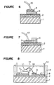
- Figure 1 is an enlarged cross-sectional view of a circuit substrate obtainable according to the present circuit substrate the present invention.
- an aluminum-copper clad foil 3 is laminated on a metallic base plate 1 by interposing an insulating layer 2 with an aluminum foil 5 being formed at the uppermost layer, wherein the aluminum-copper clad foil 3 has a roughness 4 in average of the surface in contact with the insulating layer.
- an aluminum-copper clad foil 3 is formed on the base plate 1 by interposing the insulating layer with a copper foil 6 disposing at the uppermost layer, wherein the clad foil has a roughness 4 in average at the surface in contact with the insulating layer.
- Figure 3 is an enlarged cross-sectional view showing a circuit substrate for mounting a semiconductor element wherein a semiconductor element and other electric devices are mounted on it.
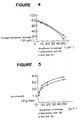
- Figures 4 and 5 respectively show relations among the voltage breakdown strength, the peel strength and the roughness Rz in average of the surfaces in contact with the insulating layer of the aluminum-copper clad foils.
- metallic base plate 1 used for the circuit substrate of the present invention aluminum, aluminum alloy, copper, copper alloy, iron, stainless steel and so on having good thermal conductivity can be used.
- a metallic base plate 1 having a thickness in a range of 0.5 mm-3.0 mm is generally used, but it is not limited thereto.
- the insulating layer 2 used for the present invention may be an insulating layer of high molecular resin which may contain ceramics or inorganic filler, a high molecular resin layer containing glass fibers or a heat-resisting an insulating layer of high molecular resin.
- the thickness of the insulating layer 2 is not particularly limited unless failure of insulation takes place. Generally, an insulating layer having a thickness of 20 ⁇ m or more is used.
- inorganic powder used for the insulating layer 2 alumina, silica, beryllia, boron nitride, magnesia, silicon nitride, aluminum nitride, silicon carbide or the like may be used.
- As the high molecular resin epoxy resin, phenol resin, polyimide resin and various kinds of engineering plastics may be used.
- pure aluminum and aluminum alloy used for an extensible material of aluminum alloy in the JIS Rule (Aluminum Handbook, edited by Shadan Hojin Keikinzoku Kyokai, The 4th Edition, 1990, p.15, Table 2.1 ) can be used.
- the major elements incorporated in the aluminum alloy are Cu, Mn, Si, Mg and so on.
- alloy which comprises at least one selected from the group consisting of an alloy containing Cu of 0.30-7.0% by weight, an alloy containing Mn of 0.1-2.0% by weight, an alloy containing Si of 2.0-15% by weight and an alloy containing Mg of 0.5-6.0% by weight.
- the hardness of pure aluminum is soft and the extension property is high, it deforms at the time of wire bonding and there causes sinking of the wire used.
- an aluminum alloy foil is used, an amount of sinking of the aluminum alloy foil is small. Accordingly, it is possible to connect a lead wire under wide wire bonding conditions (an output and a bonding time).
- the aluminum-copper clad foil is prepared by a plating method or a rolling method.
- plating method zinc, tin or nickel may be plated between an aluminum layer and a copper layer in order to increase the bonding strength between aluminum and copper.
- zinc or tin is subjected to substituting plating with a thickness of 10 ⁇ -1 ⁇ m as a substituting layer between the aluminum layer and the copper layer, and then copper plating is conducted at a thickness of about 5 ⁇ m-900 ⁇ m, an excellent bonding force is obtainable between the aluminum layer and the copper layer in comparison with a technique that nickel plating is conducted between the aluminum layer and the copper layer.
- a highly reliable electric conductive circuit can be formed.
- the roughness of the surface of the copper layer can be adjusted by adjusting the density of an electric current supplied.
- an electrolytic copper foil having an average roughness of 0.5 ⁇ m-50 ⁇ m can be formed by feeding a current having a density of 4 A/dcm 2 or lower.
- an electrolytic copper foil having an average roughness of 20 ⁇ m can be formed by supplying a current having a density of 3 A/dcm 2 .
- an electrolytic copper foil having an average roughness of 10 ⁇ m can be formed by feeding a current having a density of 2 A/dcm 2 .
- the aluminum-copper clad foil is prepared by a rolling method, it is possible to obtain a clad foil having a large thickness which is suitable for a large current. Further, the rolling method provides a clad foil having a high bonding strength at the interface and durable to corrosion at the interface and a clad foil comprising a copper foil of high purity.
- the thickness of the aluminum-copper clad foil 3 of the present invention is not in particular limited.
- the thickness of the clad foil is preferably in a range of 35 ⁇ m-1,000 ⁇ m for use for a large current.
- the thickness of the clad foil is desirably in a range of 9 ⁇ m-70 ⁇ m for use for a small current.
- the thickness of the aluminum foil is preferably in a range of 20 ⁇ m-80 ⁇ m for a large current use.
- the thickness of the aluminum foil is preferably less than 10 ⁇ m and the thickness of the copper foil is preferably in a range of 1 ⁇ m-100 ⁇ m.
- the thickness of the aluminum foil is more than 10 ⁇ m, accuracy in the width of a circuit is poor, whereby it is difficult to form a fine circuit because an amount of side etching in an etching operation is large.
- the roughness in average of the surface in contact with the insulating layer of the aluminum-copper clad foil 3 used for the present invention is in a range of 0.5 ⁇ m-50 ⁇ m.
- the roughness in average is less than 0.5 ⁇ m, the bonding strength to the insulating layer 2 is small, and the aluminum-copper clad foil 3 is easily peeled off.
- the roughness exceeds 50 ⁇ m, there occurs concentration of an electric field at the top of projections of concave and recess portions of the surface of the clad foil, and the voltage breakdown characteristic is greatly reduced.
- the roughness in average of the surface in contact with the insulating layer of the aluminum-copper clad foil 3 is in a range of 10 ⁇ m-50 ⁇ m.
- the roughness in average of the surface in contact with the insulating layer of the clad foil is in a range of 0.5 ⁇ m-20 ⁇ m. In particular, it is preferable that the roughness in a range of 0.5 ⁇ m-10 ⁇ m in use for a high voltage.
- the roughness in average is in a range of 10 ⁇ m-20 ⁇ m.
- the thickness of the surface of the clad foil can be adjusted by controlling the density of an electric current when the copper foil is formed by the electrolytic plating as described above. Further, the roughness can be adjusted by mechanically polishing or chemically polishing. In particular, the latter methods are used for forming a roughened surface of the aluminum foil because electrolytic plating is not used for the aluminum foil.
- a wire bonding portion of the aluminum-copper clad foil in the circuit substrate for mounting a semiconductor element of the present invention is classified into two cases: the aluminum foil being placed at the top surface ( Figure 6 ) and the copper foil being placed at the top surface ( Figure 7 ).
- the bonding portion is formed of a bonding wire and an aluminum foil.
- the roughness in average of the surface of the aluminum foil is 10 ⁇ m-1 ⁇ m.
- a molten portion at the bonding portion of the bonding wire can not completely fill the uneven surface at the bonding portion of the aluminum foil, whereby there takes place a non-melt portion. This may cause failure of bonding and reliability on the bonding decreases.
- the roughness is less than 1 ⁇ m, the surface area of contact between the molten portion of the bonding wire and the bonding area of the aluminum foil is small. The penetration of the molten portion into the bonding area of the aluminum foil is insufficient and the bonding strength is small. Accordingly, reliability is low.
- Figure 3 is a cross-sectional view of a circuit substrate for mounting a semiconductor element, on which a semiconductor element and other electrical devices are mounted.
- the circuit substrate was prepared by applying silica-containing epoxy resin as an insulating layer 2 at a thickness of 100 ⁇ m on an aluminum substrate as a metallic base plate 1 having a thickness of 1.5 mm, and by bonding an aluminum-copper clad foil 3 comprising 40 ⁇ m of an aluminum foil - 85 ⁇ m of a copper foil so as to place an aluminum foil 5 at the top surface.
- the clad foil used was such one that the copper is formed on the aluminum foil by electrolysis and the roughness in average (Rz) of the surface in contact with the insulating layer was 15 ⁇ m (measured by a surface roughness tester "Surfcoder", manufactured by Kosaka Kenkyusho).
- a resist was applied by a screen printing method on the circuit substrate having the same construction as in Figure 1 (the thickness of the aluminum substrate: 1.5 mm, the thickness of insulating layer: 100 ⁇ m and the thickness of the aluminum-copper clad foil: 40 ⁇ m-85 ⁇ m).
- Etching is conducted with ferric chloride to the aluminum-copper clad foil 3 to form a circuit.
- the resist was removed.
- a resist was again applied to portions which require an aluminum pad.
- An etching solution capable of selectively dissolving aluminum such as an alkali etching solution was used to remove unnecessary aluminum portions to expose copper foil portions.
- a semiconductor, a tip resistor and so on were mounted on copper conductive portions 8 of the circuit by means of solder 7, and the semiconductor element 11 and the aluminum pad 9 were connected by a wire 10 as an aluminum lead wire by using an ultrasonic vibration method.
- Silica-containing epoxy resin as the insulating layer 2 was applied to each of metallic base plates 1 of aluminum of 1.5 mm thick at a thickness of 100 ⁇ m.
- Electrolytic clad foils comprising aluminum 40 ⁇ m-copper 85 ⁇ m and rolled clad foils 3 are respectively bonded to the circuit substrates so as to place aluminum foils 5 at the top surface.
- the voltage breakdown strength of the samples were measured by using model TOS 8700 (Kikusui Denshi Kogyo Kabushiki Kaisha) in accordance with JIS C-2110.
- Figure 4 shows the relation between the roughness in average of the surface in contact with the insulating layer of the clad foil and voltage breakdown strength.
- Silica-containing epoxy resin as the insulating layer 2 was coated at a thickness of 100 ⁇ m on each of metallic base plates of the aluminum having a thickness of 1.5 mm.
- Electrolytic clad foils comprising aluminum 40 ⁇ m-copper 85 ⁇ m and rolled clad foils 3 were respectively bonded on the metallic base plates 1 so as to place aluminum foils 5 at the top surface to prepare samples of circuit substrates.
- the peel strength was measured for each of the samples by using Tensilon U-1160 (Toyo Boldwin Kabushiki kaisha) in accordance with JIS C-6481.
- Figure 5 shows the relation of the roughness in average of the surface in contact with the insulating layer of the clad foils and the voltage breakdown strength.
- the surface of the aluminum foils of the circuit substrates prepared in accordance with Example 3 was polished by using a SiC buff roll (tradename, Ultrasuper) manufactured by Kurenoton.
- the surface roughness of the samples were measured in the same manner as in Example 1.
- the roughness in average Rz was 9.2 ⁇ m.
- semiconductor elements were mounted on the samples and wire bonding of 10,000 aluminum wires of 300 ⁇ m thick was conducted by using an ultrasonic wire bonder (wire bonder USW-5Z60S by Choonpa Kogyo Kaisha). As a result of tests, there was found no failure of bonding.
- Samples of circuit substrate in which the roughness in average Rz of the aluminum surface was 12 ⁇ m were prepared in the same manner as in Example 3.
- Semiconductor elements were mounted on the samples and wire bonding of 10,000 gold wires of 25 ⁇ m thick was conducted. As a result of testing, there were found 80 numbers of failure of wire bonding.
- Circuit substrates of Example 3 were prepared.
- a transistor bare chip 11 was attached to the circuit through a heat sink 12 by means of solder 7. Further, an electrode terminal 13 was soldered, and then, the transistor bare chip 11 was bonded to the bonding surface 9 of aluminum foil with an aluminum wire 10 of 300 ⁇ m thick by ultrasonic bonding.
- a plastic package was put on the circuit substrate with an adhesive agent, and silicone resin was used for sealing.
- transistor power modules 15 were used as controlling modules for inverter air conditioners by supplying power of AC 200 V and 20 A. As a result, they were able to withstand for a long term use without breakdown.
- a circuit substrate for mounting a semiconductor element having a high peel strength and/or a high voltage breakdown characteristic can be obtained by specifying the surface roughness of the surface in contact with the insulating layer of the aluminum-copper clad foil. Further, such circuit substrate having high reliability of wire bonding can be obtained by specifying the surface roughness of the surface opposing the insulating layer of the aluminum-copper clad foil. Further, a power module for a high voltage and a high current and operable for a long time use can be obtained by using such circuit substrate for mounting a semiconductor element.
Landscapes
- Engineering & Computer Science (AREA)
- Microelectronics & Electronic Packaging (AREA)
- Computer Hardware Design (AREA)
- Power Engineering (AREA)
- Physics & Mathematics (AREA)
- Condensed Matter Physics & Semiconductors (AREA)
- General Physics & Mathematics (AREA)
- Parts Printed On Printed Circuit Boards (AREA)
- Insulated Metal Substrates For Printed Circuits (AREA)
Description
- The present invention relates to a method for producing a circuit substrate having a mounted semiconductor element used for electric devices, communicating devices and automobiles. More particularly, the present invention relates to a method for producing a highly reliable circuit substrate having a mounted semiconductor element having an improved bonding strength between a metallic foil for forming a circuit and an insulating layer; a high resistance to voltage, and excellent wire bonding property.
- A method for preparing a hybrid integrated circuit by laminating an aluminum-copper clad foil on an insulating layer and connecting a semiconductor element to an aluminum circuit through a wire is known from
GB-A 2 125 618 -
JP-A- 59158544 -
JP-A 02025045 - There have been used a copper foil, a nickel-plated copper foil and an aluminum-copper clad foil as an electric conductive foil used for a circuit substrate for mounting a semiconductor element which is used mainly for electric devices, communication devices and automobiles. In recent years, these foils have been used in various fields, and there are demands of circuit substrates capable of high density packaging, and having a high voltage resistance property, excellent wire bonding property and providing high reliability. For instance,
U.S. Patent No. 4,521,476 discloses a process for preparing a hybrid integrated circuit substrate having a circuit which is formed of an aluminum-copper clad foil laminated on a metallic base plate through an insulating layer. Japanese Examined Patent Publication No.15153/1989 108347/1991 - It is an object of the present invention to provide a method for producing a circuit substrate having a mounted semiconductor element having a large bonding strength between a circuit of an aluminum-copper clad foil and an insulating layer, an improved voltage breakdown strength characteristic and reliable strength of wire bonding. The inventors of this application have studied on the roughness of the surface in contact with the insulating layer of the aluminum-copper clad foil, the roughness of the surface of the foil in contact with a bonding wire and the quality of an aluminum foil, which are factors influencing the above-mentioned characteristics, and have achieved the present invention by finding a circuit substrate of high reliability.
- Namely, in accordance with the present invention, there is provided a method for producing a circuit substrate having a mounted semiconductor element having an aluminum-copper clad foil laminated on a metallic base plate by interposing an insulating layer, characterized in that the roughness in average of the surface in contact with the insulating layer of the aluminum-copper clad foil is in a range of from 0.5 µm to 50 µm as further defined by
claim 1. - In the present invention, the aluminum-copper clad foil is such one that a copper foil is formed on an aluminum foil by electrolytic plating, or the clad foil is prepared by a rolling method. The aluminum foil is made of pure aluminum including more than 99.0% by weight of aluminum or made of an aluminum alloy.
- The roughness in average of the surface opposing the surface in contact with the insulating layer of the aluminum-copper clad foil is 1 µm to 10 µm
- Further, there is provided a power module in which a semiconductor element is mounted on a circuit substrate comprising an aluminum-copper clad foil whose roughness in average of the surface in contact with the insulating layer is in a range of from 0.5 µm to 50 µm, the semiconductor element and a circuit formed in the circuit element are connected by wire bonding and arranged in a package such as a plastic material, and are sealed with an insulating material such as silicone resin.
- In drawings:
-
Figure 1 is an enlarged cross-sectional view of a circuit substrate comprising an aluminum-copper clad foil in which an aluminum foil is formed at the top surface; -
Figure 2 is an enlarged cross-sectional view of another circuit substrate comprising an aluminum-copper clad foil in which a copper foil is formed at the top surface; -
Figure 3 is an enlarged cross-sectional view of a circuit substrate on which an electric conductive circuit is formed and a semiconductor element is mounted; -
Figure 4 is a graph showing relations between voltage breakdown strength and roughness in average of surfaces in contact with the insulating layer of aluminum-copper clad foils; -
Figure 5 is a graph showing relations between peel strength and roughness in average of surfaces in contact with the insulating layer of aluminum-copper clad foils; -
Figure 6 is an enlarged cross-sectional view showing a wire bonded portion of the aluminum-copper clad foil (an aluminum layer at the top) of the present invention; -
Figure 7 is an enlarged cross-sectional view showing a wire bonded portion of the aluminum-copper clad foil (copper foil at the top) of the present invention; and -
Figure 8 is an enlarged cross-sectional view showing a power module obtainable according to the present invention. - In the following, preferred embodiments of the invention will be described in more detail with reference to the drawings.
- In description, the roughness in average of the surface is expressed by Rz which is defined in JIS (Japanese Industrial Standard) -B0601.
-
Figure 1 is an enlarged cross-sectional view of a circuit substrate obtainable according to the present circuit substrate the present invention. InFigure 1 , an aluminum-copper clad foil 3 is laminated on ametallic base plate 1 by interposing aninsulating layer 2 with analuminum foil 5 being formed at the uppermost layer, wherein the aluminum-copper clad foil 3 has aroughness 4 in average of the surface in contact with the insulating layer. - In
Figure 2 , an aluminum-copper clad foil 3 is formed on thebase plate 1 by interposing the insulating layer with acopper foil 6 disposing at the uppermost layer, wherein the clad foil has aroughness 4 in average at the surface in contact with the insulating layer. -
Figure 3 is an enlarged cross-sectional view showing a circuit substrate for mounting a semiconductor element wherein a semiconductor element and other electric devices are mounted on it.Figures 4 and 5 respectively show relations among the voltage breakdown strength, the peel strength and the roughness Rz in average of the surfaces in contact with the insulating layer of the aluminum-copper clad foils. - As a
metallic base plate 1 used for the circuit substrate of the present invention, aluminum, aluminum alloy, copper, copper alloy, iron, stainless steel and so on having good thermal conductivity can be used. Ametallic base plate 1 having a thickness in a range of 0.5 mm-3.0 mm is generally used, but it is not limited thereto. - The
insulating layer 2 used for the present invention may be an insulating layer of high molecular resin which may contain ceramics or inorganic filler, a high molecular resin layer containing glass fibers or a heat-resisting an insulating layer of high molecular resin. The thickness of theinsulating layer 2 is not particularly limited unless failure of insulation takes place. Generally, an insulating layer having a thickness of 20 µm or more is used. As inorganic powder used for theinsulating layer 2, alumina, silica, beryllia, boron nitride, magnesia, silicon nitride, aluminum nitride, silicon carbide or the like may be used. As the high molecular resin, epoxy resin, phenol resin, polyimide resin and various kinds of engineering plastics may be used. - As the material of aluminum of the aluminum-
copper clad foil 3 used for the present invention, pure aluminum and aluminum alloy used for an extensible material of aluminum alloy in the JIS Rule (Aluminum Handbook, edited by Shadan Hojin Keikinzoku Kyokai, The 4th Edition, 1990, p.15, Table 2.1) can be used. The major elements incorporated in the aluminum alloy are Cu, Mn, Si, Mg and so on. There can be used alloy which comprises at least one selected from the group consisting of an alloy containing Cu of 0.30-7.0% by weight, an alloy containing Mn of 0.1-2.0% by weight, an alloy containing Si of 2.0-15% by weight and an alloy containing Mg of 0.5-6.0% by weight. - Since the hardness of pure aluminum is soft and the extension property is high, it deforms at the time of wire bonding and there causes sinking of the wire used. When an aluminum alloy foil is used, an amount of sinking of the aluminum alloy foil is small. Accordingly, it is possible to connect a lead wire under wide wire bonding conditions (an output and a bonding time).
- The aluminum-copper clad foil is prepared by a plating method or a rolling method. In the case of plating method, zinc, tin or nickel may be plated between an aluminum layer and a copper layer in order to increase the bonding strength between aluminum and copper. When zinc or tin is subjected to substituting plating with a thickness of 10 Å-1 µm as a substituting layer between the aluminum layer and the copper layer, and then copper plating is conducted at a thickness of about 5 µm-900 µm, an excellent bonding force is obtainable between the aluminum layer and the copper layer in comparison with a technique that nickel plating is conducted between the aluminum layer and the copper layer. Thus, a highly reliable electric conductive circuit can be formed.
- When the copper foil is formed by electrolytics plating, the roughness of the surface of the copper layer can be adjusted by adjusting the density of an electric current supplied. For instance, an electrolytic copper foil having an average roughness of 0.5 µm-50 µm can be formed by feeding a current having a density of 4 A/dcm2 or lower. Further, an electrolytic copper foil having an average roughness of 20 µm can be formed by supplying a current having a density of 3 A/dcm2. Further, an electrolytic copper foil having an average roughness of 10 µm can be formed by feeding a current having a density of 2 A/dcm2.
- When the aluminum-copper clad foil is prepared by a rolling method, it is possible to obtain a clad foil having a large thickness which is suitable for a large current. Further, the rolling method provides a clad foil having a high bonding strength at the interface and durable to corrosion at the interface and a clad foil comprising a copper foil of high purity.
- The thickness of the aluminum-
copper clad foil 3 of the present invention is not in particular limited. For instance, the thickness of the clad foil is preferably in a range of 35 µm-1,000 µm for use for a large current. On the other hand, the thickness of the clad foil is desirably in a range of 9 µm-70 µm for use for a small current. The thickness of the aluminum foil is preferably in a range of 20 µm-80 µm for a large current use. However, when a fine circuit having the width of circuit of 200 µm or less is to be prepared, the thickness of the aluminum foil is preferably less than 10 µm and the thickness of the copper foil is preferably in a range of 1 µm-100 µm. - When the thickness of the aluminum foil is more than 10 µm, accuracy in the width of a circuit is poor, whereby it is difficult to form a fine circuit because an amount of side etching in an etching operation is large.
- The roughness in average of the surface in contact with the insulating layer of the aluminum-copper clad
foil 3 used for the present invention is in a range of 0.5 µm-50 µm. When the roughness in average is less than 0.5 µm, the bonding strength to the insulatinglayer 2 is small, and the aluminum-copper cladfoil 3 is easily peeled off. On the other hand, when the roughness exceeds 50 µm, there occurs concentration of an electric field at the top of projections of concave and recess portions of the surface of the clad foil, and the voltage breakdown characteristic is greatly reduced. - When the aluminum-copper clad foil is used for a field which requires a high peel strength, it is preferably that the roughness in average of the surface in contact with the insulating layer of the aluminum-copper clad
foil 3 is in a range of 10 µm-50 µm. On the other hand, when it is used for a field requiring a high voltage breakdown characteristic, it is preferable that the roughness in average of the surface in contact with the insulating layer of the clad foil is in a range of 0.5 µm-20 µm. In particular, it is preferable that the roughness in a range of 0.5 µm-10 µm in use for a high voltage. On the other hand, when both peel strength and voltage breakdown characteristics are required, it is preferable that the roughness in average is in a range of 10 µm-20 µm. The thickness of the surface of the clad foil can be adjusted by controlling the density of an electric current when the copper foil is formed by the electrolytic plating as described above. Further, the roughness can be adjusted by mechanically polishing or chemically polishing. In particular, the latter methods are used for forming a roughened surface of the aluminum foil because electrolytic plating is not used for the aluminum foil. - A wire bonding portion of the aluminum-copper clad foil in the circuit substrate for mounting a semiconductor element of the present invention is classified into two cases: the aluminum foil being placed at the top surface (
Figure 6 ) and the copper foil being placed at the top surface (Figure 7 ). In either case, the bonding portion is formed of a bonding wire and an aluminum foil. However, there is no change in the relation among the roughness in average of the surface in contact with the insulating layer of the aluminum-copper clad foil, the voltage breakdown characteristic and the bonding strength. The roughness in average of the surface of the aluminum foil is 10 µm-1 µm. When the roughness exceeds 10 µm, a molten portion at the bonding portion of the bonding wire can not completely fill the uneven surface at the bonding portion of the aluminum foil, whereby there takes place a non-melt portion. This may cause failure of bonding and reliability on the bonding decreases. On the other hand, when the roughness is less than 1 µm, the surface area of contact between the molten portion of the bonding wire and the bonding area of the aluminum foil is small. The penetration of the molten portion into the bonding area of the aluminum foil is insufficient and the bonding strength is small. Accordingly, reliability is low. -
Figure 3 is a cross-sectional view of a circuit substrate for mounting a semiconductor element, on which a semiconductor element and other electrical devices are mounted. - The circuit substrate was prepared by applying silica-containing epoxy resin as an insulating
layer 2 at a thickness of 100 µm on an aluminum substrate as ametallic base plate 1 having a thickness of 1.5 mm, and by bonding an aluminum-copper cladfoil 3 comprising 40 µm of an aluminum foil - 85 µm of a copper foil so as to place analuminum foil 5 at the top surface. The clad foil used was such one that the copper is formed on the aluminum foil by electrolysis and the roughness in average (Rz) of the surface in contact with the insulating layer was 15 µm (measured by a surface roughness tester "Surfcoder", manufactured by Kosaka Kenkyusho). - Then, a resist was applied by a screen printing method on the circuit substrate having the same construction as in
Figure 1 (the thickness of the aluminum substrate: 1.5 mm, the thickness of insulating layer: 100 µm and the thickness of the aluminum-copper clad foil: 40 µm-85 µm). Etching is conducted with ferric chloride to the aluminum-copper cladfoil 3 to form a circuit. The resist was removed. A resist was again applied to portions which require an aluminum pad. An etching solution capable of selectively dissolving aluminum such as an alkali etching solution was used to remove unnecessary aluminum portions to expose copper foil portions. After the resist was removed, a semiconductor, a tip resistor and so on were mounted on copperconductive portions 8 of the circuit by means ofsolder 7, and thesemiconductor element 11 and thealuminum pad 9 were connected by awire 10 as an aluminum lead wire by using an ultrasonic vibration method. - Silica-containing epoxy resin as the insulating
layer 2 was applied to each ofmetallic base plates 1 of aluminum of 1.5 mm thick at a thickness of 100 µm. Electrolytic cladfoils comprising aluminum 40 µm-copper 85 µm and rolledclad foils 3 are respectively bonded to the circuit substrates so as to place aluminum foils 5 at the top surface. The voltage breakdown strength of the samples were measured by using model TOS 8700 (Kikusui Denshi Kogyo Kabushiki Kaisha) in accordance with JIS C-2110.Figure 4 shows the relation between the roughness in average of the surface in contact with the insulating layer of the clad foil and voltage breakdown strength. - Silica-containing epoxy resin as the insulating
layer 2 was coated at a thickness of 100 µm on each of metallic base plates of the aluminum having a thickness of 1.5 mm. Electrolytic cladfoils comprising aluminum 40 µm-copper 85 µm and rolledclad foils 3 were respectively bonded on themetallic base plates 1 so as to place aluminum foils 5 at the top surface to prepare samples of circuit substrates. The peel strength was measured for each of the samples by using Tensilon U-1160 (Toyo Boldwin Kabushiki kaisha) in accordance with JIS C-6481.Figure 5 shows the relation of the roughness in average of the surface in contact with the insulating layer of the clad foils and the voltage breakdown strength. - The surface of the aluminum foils of the circuit substrates prepared in accordance with Example 3 was polished by using a SiC buff roll (tradename, Ultrasuper) manufactured by Kurenoton. The surface roughness of the samples were measured in the same manner as in Example 1. As a result, the roughness in average Rz was 9.2 µm. Then, semiconductor elements were mounted on the samples and wire bonding of 10,000 aluminum wires of 300 µm thick was conducted by using an ultrasonic wire bonder (wire bonder USW-5Z60S by Choonpa Kogyo Kaisha). As a result of tests, there was found no failure of bonding.
- Samples of circuit substrate in which the roughness in average Rz of the aluminum surface was 12 µm were prepared in the same manner as in Example 3. Semiconductor elements were mounted on the samples and wire bonding of 10,000 gold wires of 25 µm thick was conducted. As a result of testing, there were found 80 numbers of failure of wire bonding.
- Circuit substrates of Example 3 were prepared. A transistor
bare chip 11 was attached to the circuit through aheat sink 12 by means ofsolder 7. Further, anelectrode terminal 13 was soldered, and then, the transistorbare chip 11 was bonded to thebonding surface 9 of aluminum foil with analuminum wire 10 of 300 µm thick by ultrasonic bonding. A plastic package was put on the circuit substrate with an adhesive agent, and silicone resin was used for sealing. Thus obtainedtransistor power modules 15 were used as controlling modules for inverter air conditioners by supplying power ofAC 200 V and 20 A. As a result, they were able to withstand for a long term use without breakdown. - In accordance with the present invention, a circuit substrate for mounting a semiconductor element having a high peel strength and/or a high voltage breakdown characteristic can be obtained by specifying the surface roughness of the surface in contact with the insulating layer of the aluminum-copper clad foil. Further, such circuit substrate having high reliability of wire bonding can be obtained by specifying the surface roughness of the surface opposing the insulating layer of the aluminum-copper clad foil. Further, a power module for a high voltage and a high current and operable for a long time use can be obtained by using such circuit substrate for mounting a semiconductor element.
Claims (4)
- A method for producing a circuit substrate having a mounted semiconductor element reliably wire bonded to the circuit substrate, whereby said method comprises the following steps:(a) providing a circuit substrate by laminating an aluminum-copper clad foil (3) on a metallic base plate (1) by interposing an insulating layer (2) between said aluminum-copper clad foil and said metallic base plate, whereby the roughness (4) according to JIS B0601 in average of a surface of the aluminum-copper clad foil, which surface is contacted with the insulating layer (2), is in a range of from 0.5 µm to 50 µm;(b) providing a wire bonding portion on the exposed portion of the aluminum foil;(c) providing the surface of the wire bonding portion of the aluminum foil included in the aluminum-copper clad foil (3), which surface is opposite to said surface contacted with the insulating layer,with a roughness according to JIS B0601 in average being in a range of from 1.0 µm to 10 µm(d) mounting the semiconductor element on the circuit substrate; and(e) connecting said semiconductor element to said circuit substrate by wire bonding to said surface of the aluminum foil having the roughness according to JIS B0601 in average in a range of from 1.0 µm to 10µm.
- The method according to Claim 1, wherein the roughness in average of the surface in contact with the insulating layer of the aluminum-copper clad foil is in a range of from 0.5 µm to 20 µm.
- The method according to Claim 1 or 2, wherein the aluminum-copper clad foil is a clad foil obtained by electrolytic plating a copper layer on an aluminum foil.
- The method according to any one of Claims 1 to 3, wherein aluminum in the aluminum-copper clad foil is an aluminum alloy which comprises at least one selected from the group consisting of an aluminum alloy containing Cu of 0.30 to 7.0 % by weight, an aluminum alloy containing Mn of 0.1 to 2.0 % by weight, an aluminum alloy containing Si of 2.0 to 15 % by weight and an aluminum alloy containing Mg of 0.5 to 6.0 % by weight.
Applications Claiming Priority (9)
| Application Number | Priority Date | Filing Date | Title |
|---|---|---|---|
| JP20614691 | 1991-07-24 | ||
| JP20614691A JP3156798B2 (en) | 1991-07-24 | 1991-07-24 | Circuit board for semiconductor mounting |
| JP20615191 | 1991-07-24 | ||
| JP3206151A JPH0529371A (en) | 1991-07-24 | 1991-07-24 | Hybrid integrated circuit |
| JP3208780A JP2899143B2 (en) | 1991-07-26 | 1991-07-26 | Semiconductor mounted circuit board |
| JP20878091 | 1991-07-26 | ||
| JP3730792 | 1992-01-28 | ||
| JP3730792A JP2957791B2 (en) | 1992-01-28 | 1992-01-28 | Semiconductor mounted circuit board |
| EP92112599A EP0525644A1 (en) | 1991-07-24 | 1992-07-23 | Circuit substrate for mounting a semiconductor element |
Related Parent Applications (2)
| Application Number | Title | Priority Date | Filing Date |
|---|---|---|---|
| EP92112599.3 Division | 1992-07-23 | ||
| EP92112599A Division EP0525644A1 (en) | 1991-07-24 | 1992-07-23 | Circuit substrate for mounting a semiconductor element |
Publications (2)
| Publication Number | Publication Date |
|---|---|
| EP1132961A1 EP1132961A1 (en) | 2001-09-12 |
| EP1132961B1 true EP1132961B1 (en) | 2011-01-05 |
Family
ID=27460395
Family Applications (2)
| Application Number | Title | Priority Date | Filing Date |
|---|---|---|---|
| EP92112599A Ceased EP0525644A1 (en) | 1991-07-24 | 1992-07-23 | Circuit substrate for mounting a semiconductor element |
| EP01100741A Expired - Lifetime EP1132961B1 (en) | 1991-07-24 | 1992-07-23 | Method for producing a circuit substrate having a mounted semiconductor element |
Family Applications Before (1)
| Application Number | Title | Priority Date | Filing Date |
|---|---|---|---|
| EP92112599A Ceased EP0525644A1 (en) | 1991-07-24 | 1992-07-23 | Circuit substrate for mounting a semiconductor element |
Country Status (3)
| Country | Link |
|---|---|
| US (1) | US5362926A (en) |
| EP (2) | EP0525644A1 (en) |
| DE (1) | DE69233801D1 (en) |
Families Citing this family (35)
| Publication number | Priority date | Publication date | Assignee | Title |
|---|---|---|---|---|
| DE4123911C1 (en) * | 1991-07-18 | 1993-01-14 | Doduco Gmbh + Co Dr. Eugen Duerrwaechter, 7530 Pforzheim, De | |
| US5673695A (en) * | 1995-08-02 | 1997-10-07 | Ep Technologies, Inc. | Methods for locating and ablating accessory pathways in the heart |
| US6175084B1 (en) * | 1995-04-12 | 2001-01-16 | Denki Kagaku Kogyo Kabushiki Kaisha | Metal-base multilayer circuit substrate having a heat conductive adhesive layer |
| DE19722355A1 (en) * | 1997-05-28 | 1998-12-03 | Bosch Gmbh Robert | Method of manufacturing electrical assemblies and electrical assembly |
| US6204454B1 (en) * | 1997-12-27 | 2001-03-20 | Tdk Corporation | Wiring board and process for the production thereof |
| WO2001050822A1 (en) * | 1999-12-30 | 2001-07-12 | Lear Automotive (Eeds) Spain, S.L. | Composite material for obtaining printed circuits, production method thereof and printed circuit board obtained from said composite material |
| US20040231141A1 (en) * | 2001-07-06 | 2004-11-25 | Masaru Nishinaka | Laminate and its producing method |
| TW200404484A (en) * | 2002-09-02 | 2004-03-16 | Furukawa Circuit Foil | Copper foil for soft circuit board package module, for plasma display, or for radio-frequency printed circuit board |
| JP3740116B2 (en) * | 2002-11-11 | 2006-02-01 | 三菱電機株式会社 | Molded resin encapsulated power semiconductor device and manufacturing method thereof |
| SG157957A1 (en) * | 2003-01-29 | 2010-01-29 | Interplex Qlp Inc | Package for integrated circuit die |
| JP4346333B2 (en) * | 2003-03-26 | 2009-10-21 | 新光電気工業株式会社 | Method for manufacturing multilayer circuit board incorporating semiconductor element |
| DE10341453A1 (en) * | 2003-09-09 | 2005-03-31 | Robert Bosch Gmbh | circuit support |
| US20060006526A1 (en) * | 2004-07-06 | 2006-01-12 | Coronati John M | Thermal interposer for cooled electrical packages |
| KR100646093B1 (en) | 2004-12-17 | 2006-11-15 | 엘지이노텍 주식회사 | Light emitting device package |
| JP4595665B2 (en) * | 2005-05-13 | 2010-12-08 | 富士電機システムズ株式会社 | Wiring board manufacturing method |
| US7972710B2 (en) | 2006-08-31 | 2011-07-05 | Antaya Technologies Corporation | Clad aluminum connector |
| JP5192163B2 (en) * | 2007-03-23 | 2013-05-08 | 住友電工デバイス・イノベーション株式会社 | Semiconductor device |
| JP4498378B2 (en) * | 2007-03-30 | 2010-07-07 | 三洋電機株式会社 | Substrate and manufacturing method thereof, circuit device and manufacturing method thereof |
| KR100881695B1 (en) * | 2007-08-17 | 2009-02-06 | 삼성전기주식회사 | Printed circuit board with embedded capacitors and method for manufacturing thereof |
| US8132321B2 (en) * | 2008-08-13 | 2012-03-13 | Unimicron Technology Corp. | Method for making embedded circuit structure |
| WO2010117023A1 (en) * | 2009-04-09 | 2010-10-14 | 日本発條株式会社 | Metal-based circuit board and method for producing same |
| DE102009033029A1 (en) * | 2009-07-02 | 2011-01-05 | Electrovac Ag | Electronic device |
| EP2315242A1 (en) * | 2009-10-23 | 2011-04-27 | ABB Technology AG | Circuit arrangement and manufacturing method thereof |
| FR2969899B1 (en) * | 2010-12-23 | 2012-12-21 | Valeo Sys Controle Moteur Sas | PRINTED CIRCUIT WITH INSULATED METAL SUBSTRATE |
| JP6144003B2 (en) * | 2011-08-29 | 2017-06-07 | 富士通株式会社 | Wiring structure and manufacturing method thereof, electronic device and manufacturing method thereof |
| DE102012102090A1 (en) * | 2012-01-31 | 2013-08-01 | Curamik Electronics Gmbh | Thermoelectric generator module, metal-ceramic substrate and method for producing a metal-ceramic substrate |
| KR20140008923A (en) * | 2012-07-13 | 2014-01-22 | 삼성전기주식회사 | Coreless substrate and method of manufacturing the same |
| JP6099453B2 (en) * | 2012-11-28 | 2017-03-22 | Dowaメタルテック株式会社 | Electronic component mounting substrate and manufacturing method thereof |
| JP6192561B2 (en) * | 2014-02-17 | 2017-09-06 | 三菱電機株式会社 | Power semiconductor device |
| JP2015220341A (en) * | 2014-05-19 | 2015-12-07 | 三菱電機株式会社 | Metal base substrate, power module, and manufacturing method of metal base substrate |
| JP6867102B2 (en) * | 2014-10-22 | 2021-04-28 | Jx金属株式会社 | Manufacturing method of copper heat dissipation material, copper foil with carrier, connector, terminal, laminate, shield material, printed wiring board, metal processing member, electronic device, and printed wiring board |
| US9408301B2 (en) * | 2014-11-06 | 2016-08-02 | Semiconductor Components Industries, Llc | Substrate structures and methods of manufacture |
| US9397017B2 (en) * | 2014-11-06 | 2016-07-19 | Semiconductor Components Industries, Llc | Substrate structures and methods of manufacture |
| DE102015111667A1 (en) | 2015-07-17 | 2017-01-19 | Rogers Germany Gmbh | Substrate for electrical circuits and method for producing such a substrate |
| CN111825947B (en) * | 2019-04-22 | 2021-08-27 | 广东生益科技股份有限公司 | Resin composition for metal substrate, resin glue solution containing resin composition and metal-based copper-clad laminate |
Citations (2)
| Publication number | Priority date | Publication date | Assignee | Title |
|---|---|---|---|---|
| JPS5739548A (en) * | 1980-08-21 | 1982-03-04 | Toshiba Corp | Semiconductor device |
| JPH0225045A (en) * | 1988-07-13 | 1990-01-26 | Oki Electric Ind Co Ltd | Semiconductor device |
Family Cites Families (13)
| Publication number | Priority date | Publication date | Assignee | Title |
|---|---|---|---|---|
| US3328275A (en) * | 1963-12-18 | 1967-06-27 | Revere Copper & Brass Inc | Treatment of copper to form a dendritic surface |
| JPS5933894A (en) * | 1982-08-19 | 1984-02-23 | 電気化学工業株式会社 | Method of producing hybrid integrated circuit board |
| JPS59158544A (en) * | 1983-03-01 | 1984-09-08 | Niles Parts Co Ltd | Circuit substrate and manufacture thereof |
| US4767674A (en) * | 1984-01-27 | 1988-08-30 | Dainichi-Nippon Cables, Ltd. | Metal cored board and method for manufacturing same |
| JPS61207044A (en) * | 1985-03-12 | 1986-09-13 | Showa Denko Kk | Formation of circuit of thermal spraying substrate |
| JPS6254947A (en) * | 1985-09-04 | 1987-03-10 | Hitachi Cable Ltd | Metal strip for lead frame |
| JPH0639155B2 (en) * | 1986-02-21 | 1994-05-25 | 名幸電子工業株式会社 | Method for manufacturing copper clad laminate |
| DE3786600T2 (en) * | 1986-05-30 | 1993-11-04 | Furukawa Electric Co Ltd | MULTILAYER PRINTED CIRCUIT AND METHOD FOR THEIR PRODUCTION. |
| JPH064143B2 (en) * | 1987-07-08 | 1994-01-19 | 川崎重工業株式会社 | Discharge structure of ball mill for coal / water slurry |
| JPH01101697A (en) * | 1987-10-14 | 1989-04-19 | Sumitomo Electric Ind Ltd | Manufacture of flexible printed wiring board |
| JPH01272183A (en) * | 1988-04-25 | 1989-10-31 | Toshiba Corp | Ceramics circuit board |
| JP2501126B2 (en) * | 1989-09-22 | 1996-05-29 | 電気化学工業株式会社 | Bonding method of gold wire to aluminum lead terminal |
| JP2801732B2 (en) * | 1990-03-22 | 1998-09-21 | 株式会社東芝 | Cladding material for substrate wiring and method of manufacturing the same |
-
1992
- 1992-07-23 DE DE69233801T patent/DE69233801D1/en not_active Expired - Lifetime
- 1992-07-23 EP EP92112599A patent/EP0525644A1/en not_active Ceased
- 1992-07-23 EP EP01100741A patent/EP1132961B1/en not_active Expired - Lifetime
- 1992-07-24 US US07/917,971 patent/US5362926A/en not_active Expired - Lifetime
Patent Citations (2)
| Publication number | Priority date | Publication date | Assignee | Title |
|---|---|---|---|---|
| JPS5739548A (en) * | 1980-08-21 | 1982-03-04 | Toshiba Corp | Semiconductor device |
| JPH0225045A (en) * | 1988-07-13 | 1990-01-26 | Oki Electric Ind Co Ltd | Semiconductor device |
Also Published As
| Publication number | Publication date |
|---|---|
| EP1132961A1 (en) | 2001-09-12 |
| US5362926A (en) | 1994-11-08 |
| DE69233801D1 (en) | 2011-02-17 |
| EP0525644A1 (en) | 1993-02-03 |
Similar Documents
| Publication | Publication Date | Title |
|---|---|---|
| EP1132961B1 (en) | Method for producing a circuit substrate having a mounted semiconductor element | |
| EP0702408A2 (en) | Package for mounting a semiconductor device | |
| KR100382631B1 (en) | Metal-based multilayer circuit board and semiconductor module having the same | |
| EP0502887B1 (en) | Metal pin grid array package including dielectric polymer sealant | |
| EP0052920B1 (en) | Electronic circuit interconnection system | |
| JP4015023B2 (en) | ELECTRONIC CIRCUIT MEMBER, ITS MANUFACTURING METHOD, AND ELECTRONIC COMPONENT | |
| EP0249755B1 (en) | Hybrid integrated circuit apparatus | |
| EP0537965B1 (en) | Process of manufacturing a heat-conductive material | |
| US5736790A (en) | Semiconductor chip, package and semiconductor device | |
| US20030150109A1 (en) | Method of manufacturing a circuit board | |
| JP4206651B2 (en) | Circuit board with heat sink | |
| JPS59198790A (en) | Printed circuit board | |
| JP3156798B2 (en) | Circuit board for semiconductor mounting | |
| JPH0613723A (en) | Hybrid integrated circuit | |
| JP3257953B2 (en) | Method for manufacturing substrate for hybrid integrated circuit | |
| JP3174026B2 (en) | Metal-based multilayer circuit board | |
| Chung et al. | Z-axis conductive adhesive for TAB and fine pitch interconnects | |
| JP3167360B2 (en) | Manufacturing method of substrate for hybrid integrated circuit | |
| JP3420469B2 (en) | Wiring board | |
| EP4174929A1 (en) | Circuit board | |
| JPH0382142A (en) | Semiconductor device | |
| JP4318374B2 (en) | Metal base circuit board | |
| JPH10335769A (en) | Hybrid integrated circuit substrate | |
| EP0366338A2 (en) | A substrate for an electrical circuit system and a circuit system using that substrate | |
| JP2672349B2 (en) | IC lead member |
Legal Events
| Date | Code | Title | Description |
|---|---|---|---|
| PUAI | Public reference made under article 153(3) epc to a published international application that has entered the european phase |
Free format text: ORIGINAL CODE: 0009012 |
|
| 17P | Request for examination filed |
Effective date: 20010112 |
|
| AC | Divisional application: reference to earlier application |
Ref document number: 525644 Country of ref document: EP |
|
| AK | Designated contracting states |
Kind code of ref document: A1 Designated state(s): DE FR GB |
|
| AKX | Designation fees paid |
Free format text: DE FR GB |
|
| 17Q | First examination report despatched |
Effective date: 20030219 |
|
| GRAP | Despatch of communication of intention to grant a patent |
Free format text: ORIGINAL CODE: EPIDOSNIGR1 |
|
| RTI1 | Title (correction) |
Free format text: METHOD FOR PRODUCING A CIRCUIT SUBSTRATE HAVING A MOUNTED SEMICONDUCTOR ELEMENT |
|
| GRAS | Grant fee paid |
Free format text: ORIGINAL CODE: EPIDOSNIGR3 |
|
| GRAA | (expected) grant |
Free format text: ORIGINAL CODE: 0009210 |
|
| AC | Divisional application: reference to earlier application |
Ref document number: 0525644 Country of ref document: EP Kind code of ref document: P |
|
| AK | Designated contracting states |
Kind code of ref document: B1 Designated state(s): DE FR GB |
|
| REG | Reference to a national code |
Ref country code: GB Ref legal event code: FG4D |
|
| REF | Corresponds to: |
Ref document number: 69233801 Country of ref document: DE Date of ref document: 20110217 Kind code of ref document: P |
|
| REG | Reference to a national code |
Ref country code: DE Ref legal event code: R096 Ref document number: 69233801 Country of ref document: DE Effective date: 20110217 |
|
| PGFP | Annual fee paid to national office [announced via postgrant information from national office to epo] |
Ref country code: FR Payment date: 20110727 Year of fee payment: 20 |
|
| PLBE | No opposition filed within time limit |
Free format text: ORIGINAL CODE: 0009261 |
|
| STAA | Information on the status of an ep patent application or granted ep patent |
Free format text: STATUS: NO OPPOSITION FILED WITHIN TIME LIMIT |
|
| PGFP | Annual fee paid to national office [announced via postgrant information from national office to epo] |
Ref country code: GB Payment date: 20110720 Year of fee payment: 20 Ref country code: DE Payment date: 20110720 Year of fee payment: 20 |
|
| 26N | No opposition filed |
Effective date: 20111006 |
|
| REG | Reference to a national code |
Ref country code: DE Ref legal event code: R097 Ref document number: 69233801 Country of ref document: DE Effective date: 20111006 |
|
| REG | Reference to a national code |
Ref country code: DE Ref legal event code: R071 Ref document number: 69233801 Country of ref document: DE |
|
| REG | Reference to a national code |
Ref country code: DE Ref legal event code: R071 Ref document number: 69233801 Country of ref document: DE |
|
| REG | Reference to a national code |
Ref country code: GB Ref legal event code: PE20 Expiry date: 20120722 |
|
| PG25 | Lapsed in a contracting state [announced via postgrant information from national office to epo] |
Ref country code: GB Free format text: LAPSE BECAUSE OF EXPIRATION OF PROTECTION Effective date: 20120722 Ref country code: DE Free format text: LAPSE BECAUSE OF EXPIRATION OF PROTECTION Effective date: 20120724 |