JP5192163B2 - Semiconductor device - Google Patents
Semiconductor device Download PDFInfo
- Publication number
- JP5192163B2 JP5192163B2 JP2007075858A JP2007075858A JP5192163B2 JP 5192163 B2 JP5192163 B2 JP 5192163B2 JP 2007075858 A JP2007075858 A JP 2007075858A JP 2007075858 A JP2007075858 A JP 2007075858A JP 5192163 B2 JP5192163 B2 JP 5192163B2
- Authority
- JP
- Japan
- Prior art keywords
- layer
- pad
- wiring layer
- wiring
- semiconductor device
- Prior art date
- Legal status (The legal status is an assumption and is not a legal conclusion. Google has not performed a legal analysis and makes no representation as to the accuracy of the status listed.)
- Active
Links
- 239000004065 semiconductor Substances 0.000 title claims description 68
- 230000004888 barrier function Effects 0.000 claims description 39
- 150000001875 compounds Chemical class 0.000 claims description 17
- 229910008807 WSiN Inorganic materials 0.000 claims description 3
- ATJFFYVFTNAWJD-UHFFFAOYSA-N Tin Chemical compound [Sn] ATJFFYVFTNAWJD-UHFFFAOYSA-N 0.000 claims 1
- 239000010410 layer Substances 0.000 description 188
- 239000010931 gold Substances 0.000 description 67
- 229910052737 gold Inorganic materials 0.000 description 27
- 229910052782 aluminium Inorganic materials 0.000 description 26
- 238000006243 chemical reaction Methods 0.000 description 21
- 229910002601 GaN Inorganic materials 0.000 description 10
- JMASRVWKEDWRBT-UHFFFAOYSA-N Gallium nitride Chemical compound [Ga]#N JMASRVWKEDWRBT-UHFFFAOYSA-N 0.000 description 10
- 238000010586 diagram Methods 0.000 description 9
- 239000000758 substrate Substances 0.000 description 9
- NRTOMJZYCJJWKI-UHFFFAOYSA-N Titanium nitride Chemical compound [Ti]#N NRTOMJZYCJJWKI-UHFFFAOYSA-N 0.000 description 5
- PXHVJJICTQNCMI-UHFFFAOYSA-N nickel Substances [Ni] PXHVJJICTQNCMI-UHFFFAOYSA-N 0.000 description 4
- KDLHZDBZIXYQEI-UHFFFAOYSA-N palladium Substances [Pd] KDLHZDBZIXYQEI-UHFFFAOYSA-N 0.000 description 4
- 239000011347 resin Substances 0.000 description 4
- 229920005989 resin Polymers 0.000 description 4
- 238000007789 sealing Methods 0.000 description 4
- 239000010936 titanium Substances 0.000 description 4
- 230000015556 catabolic process Effects 0.000 description 3
- 229910052802 copper Inorganic materials 0.000 description 3
- 239000010949 copper Substances 0.000 description 3
- MZLGASXMSKOWSE-UHFFFAOYSA-N tantalum nitride Chemical compound [Ta]#N MZLGASXMSKOWSE-UHFFFAOYSA-N 0.000 description 3
- 229910001218 Gallium arsenide Inorganic materials 0.000 description 2
- 206010035148 Plague Diseases 0.000 description 2
- XUIMIQQOPSSXEZ-UHFFFAOYSA-N Silicon Chemical compound [Si] XUIMIQQOPSSXEZ-UHFFFAOYSA-N 0.000 description 2
- 241000607479 Yersinia pestis Species 0.000 description 2
- 230000000052 comparative effect Effects 0.000 description 2
- 238000005530 etching Methods 0.000 description 2
- 230000009477 glass transition Effects 0.000 description 2
- 239000012535 impurity Substances 0.000 description 2
- 229910000765 intermetallic Inorganic materials 0.000 description 2
- 229910052741 iridium Inorganic materials 0.000 description 2
- 238000004519 manufacturing process Methods 0.000 description 2
- 239000000463 material Substances 0.000 description 2
- 229910052759 nickel Inorganic materials 0.000 description 2
- 229910052710 silicon Inorganic materials 0.000 description 2
- 239000010703 silicon Substances 0.000 description 2
- HBMJWWWQQXIZIP-UHFFFAOYSA-N silicon carbide Chemical compound [Si+]#[C-] HBMJWWWQQXIZIP-UHFFFAOYSA-N 0.000 description 2
- 229910010271 silicon carbide Inorganic materials 0.000 description 2
- 229910052715 tantalum Inorganic materials 0.000 description 2
- 229910052719 titanium Inorganic materials 0.000 description 2
- 229910052721 tungsten Inorganic materials 0.000 description 2
- 239000010937 tungsten Substances 0.000 description 2
- -1 tungsten nitride Chemical class 0.000 description 2
- RYGMFSIKBFXOCR-UHFFFAOYSA-N Copper Chemical compound [Cu] RYGMFSIKBFXOCR-UHFFFAOYSA-N 0.000 description 1
- ZOKXTWBITQBERF-UHFFFAOYSA-N Molybdenum Chemical compound [Mo] ZOKXTWBITQBERF-UHFFFAOYSA-N 0.000 description 1
- 229910052581 Si3N4 Inorganic materials 0.000 description 1
- VYPSYNLAJGMNEJ-UHFFFAOYSA-N Silicium dioxide Chemical compound O=[Si]=O VYPSYNLAJGMNEJ-UHFFFAOYSA-N 0.000 description 1
- RTAQQCXQSZGOHL-UHFFFAOYSA-N Titanium Chemical compound [Ti] RTAQQCXQSZGOHL-UHFFFAOYSA-N 0.000 description 1
- XAGFODPZIPBFFR-UHFFFAOYSA-N aluminium Chemical compound [Al] XAGFODPZIPBFFR-UHFFFAOYSA-N 0.000 description 1
- QVGXLLKOCUKJST-UHFFFAOYSA-N atomic oxygen Chemical compound [O] QVGXLLKOCUKJST-UHFFFAOYSA-N 0.000 description 1
- 230000015572 biosynthetic process Effects 0.000 description 1
- 230000009194 climbing Effects 0.000 description 1
- 230000006378 damage Effects 0.000 description 1
- 238000000354 decomposition reaction Methods 0.000 description 1
- 230000006866 deterioration Effects 0.000 description 1
- 238000011161 development Methods 0.000 description 1
- 230000005669 field effect Effects 0.000 description 1
- PCHJSUWPFVWCPO-UHFFFAOYSA-N gold Chemical compound [Au] PCHJSUWPFVWCPO-UHFFFAOYSA-N 0.000 description 1
- 238000009413 insulation Methods 0.000 description 1
- 239000011229 interlayer Substances 0.000 description 1
- 150000002500 ions Chemical class 0.000 description 1
- GKOZUEZYRPOHIO-UHFFFAOYSA-N iridium atom Chemical compound [Ir] GKOZUEZYRPOHIO-UHFFFAOYSA-N 0.000 description 1
- 230000005012 migration Effects 0.000 description 1
- 238000013508 migration Methods 0.000 description 1
- 238000012986 modification Methods 0.000 description 1
- 230000004048 modification Effects 0.000 description 1
- 229910052750 molybdenum Inorganic materials 0.000 description 1
- 239000011733 molybdenum Substances 0.000 description 1
- 229910052760 oxygen Inorganic materials 0.000 description 1
- 239000001301 oxygen Substances 0.000 description 1
- 229910052763 palladium Inorganic materials 0.000 description 1
- 238000012545 processing Methods 0.000 description 1
- 230000001681 protective effect Effects 0.000 description 1
- 229910052594 sapphire Inorganic materials 0.000 description 1
- 239000010980 sapphire Substances 0.000 description 1
- HQVNEWCFYHHQES-UHFFFAOYSA-N silicon nitride Chemical compound N12[Si]34N5[Si]62N3[Si]51N64 HQVNEWCFYHHQES-UHFFFAOYSA-N 0.000 description 1
- 229910052814 silicon oxide Inorganic materials 0.000 description 1
- GUVRBAGPIYLISA-UHFFFAOYSA-N tantalum atom Chemical compound [Ta] GUVRBAGPIYLISA-UHFFFAOYSA-N 0.000 description 1
- WFKWXMTUELFFGS-UHFFFAOYSA-N tungsten Chemical compound [W] WFKWXMTUELFFGS-UHFFFAOYSA-N 0.000 description 1
- 229910021342 tungsten silicide Inorganic materials 0.000 description 1
Images


Classifications
-
- H—ELECTRICITY
- H01—ELECTRIC ELEMENTS
- H01L—SEMICONDUCTOR DEVICES NOT COVERED BY CLASS H10
- H01L24/00—Arrangements for connecting or disconnecting semiconductor or solid-state bodies; Methods or apparatus related thereto
- H01L24/01—Means for bonding being attached to, or being formed on, the surface to be connected, e.g. chip-to-package, die-attach, "first-level" interconnects; Manufacturing methods related thereto
- H01L24/02—Bonding areas ; Manufacturing methods related thereto
- H01L24/03—Manufacturing methods
-
- H—ELECTRICITY
- H01—ELECTRIC ELEMENTS
- H01L—SEMICONDUCTOR DEVICES NOT COVERED BY CLASS H10
- H01L24/00—Arrangements for connecting or disconnecting semiconductor or solid-state bodies; Methods or apparatus related thereto
- H01L24/01—Means for bonding being attached to, or being formed on, the surface to be connected, e.g. chip-to-package, die-attach, "first-level" interconnects; Manufacturing methods related thereto
- H01L24/02—Bonding areas ; Manufacturing methods related thereto
- H01L24/04—Structure, shape, material or disposition of the bonding areas prior to the connecting process
- H01L24/05—Structure, shape, material or disposition of the bonding areas prior to the connecting process of an individual bonding area
-
- H—ELECTRICITY
- H01—ELECTRIC ELEMENTS
- H01L—SEMICONDUCTOR DEVICES NOT COVERED BY CLASS H10
- H01L24/00—Arrangements for connecting or disconnecting semiconductor or solid-state bodies; Methods or apparatus related thereto
- H01L24/01—Means for bonding being attached to, or being formed on, the surface to be connected, e.g. chip-to-package, die-attach, "first-level" interconnects; Manufacturing methods related thereto
- H01L24/02—Bonding areas ; Manufacturing methods related thereto
- H01L24/04—Structure, shape, material or disposition of the bonding areas prior to the connecting process
- H01L24/06—Structure, shape, material or disposition of the bonding areas prior to the connecting process of a plurality of bonding areas
-
- H—ELECTRICITY
- H01—ELECTRIC ELEMENTS
- H01L—SEMICONDUCTOR DEVICES NOT COVERED BY CLASS H10
- H01L24/00—Arrangements for connecting or disconnecting semiconductor or solid-state bodies; Methods or apparatus related thereto
- H01L24/01—Means for bonding being attached to, or being formed on, the surface to be connected, e.g. chip-to-package, die-attach, "first-level" interconnects; Manufacturing methods related thereto
- H01L24/42—Wire connectors; Manufacturing methods related thereto
- H01L24/47—Structure, shape, material or disposition of the wire connectors after the connecting process
- H01L24/48—Structure, shape, material or disposition of the wire connectors after the connecting process of an individual wire connector
-
- H—ELECTRICITY
- H01—ELECTRIC ELEMENTS
- H01L—SEMICONDUCTOR DEVICES NOT COVERED BY CLASS H10
- H01L2224/00—Indexing scheme for arrangements for connecting or disconnecting semiconductor or solid-state bodies and methods related thereto as covered by H01L24/00
- H01L2224/01—Means for bonding being attached to, or being formed on, the surface to be connected, e.g. chip-to-package, die-attach, "first-level" interconnects; Manufacturing methods related thereto
- H01L2224/02—Bonding areas; Manufacturing methods related thereto
- H01L2224/0212—Auxiliary members for bonding areas, e.g. spacers
- H01L2224/02122—Auxiliary members for bonding areas, e.g. spacers being formed on the semiconductor or solid-state body
- H01L2224/02163—Auxiliary members for bonding areas, e.g. spacers being formed on the semiconductor or solid-state body on the bonding area
- H01L2224/02165—Reinforcing structures
- H01L2224/02166—Collar structures
-
- H—ELECTRICITY
- H01—ELECTRIC ELEMENTS
- H01L—SEMICONDUCTOR DEVICES NOT COVERED BY CLASS H10
- H01L2224/00—Indexing scheme for arrangements for connecting or disconnecting semiconductor or solid-state bodies and methods related thereto as covered by H01L24/00
- H01L2224/01—Means for bonding being attached to, or being formed on, the surface to be connected, e.g. chip-to-package, die-attach, "first-level" interconnects; Manufacturing methods related thereto
- H01L2224/02—Bonding areas; Manufacturing methods related thereto
- H01L2224/023—Redistribution layers [RDL] for bonding areas
-
- H—ELECTRICITY
- H01—ELECTRIC ELEMENTS
- H01L—SEMICONDUCTOR DEVICES NOT COVERED BY CLASS H10
- H01L2224/00—Indexing scheme for arrangements for connecting or disconnecting semiconductor or solid-state bodies and methods related thereto as covered by H01L24/00
- H01L2224/01—Means for bonding being attached to, or being formed on, the surface to be connected, e.g. chip-to-package, die-attach, "first-level" interconnects; Manufacturing methods related thereto
- H01L2224/02—Bonding areas; Manufacturing methods related thereto
- H01L2224/04—Structure, shape, material or disposition of the bonding areas prior to the connecting process
- H01L2224/04042—Bonding areas specifically adapted for wire connectors, e.g. wirebond pads
-
- H—ELECTRICITY
- H01—ELECTRIC ELEMENTS
- H01L—SEMICONDUCTOR DEVICES NOT COVERED BY CLASS H10
- H01L2224/00—Indexing scheme for arrangements for connecting or disconnecting semiconductor or solid-state bodies and methods related thereto as covered by H01L24/00
- H01L2224/01—Means for bonding being attached to, or being formed on, the surface to be connected, e.g. chip-to-package, die-attach, "first-level" interconnects; Manufacturing methods related thereto
- H01L2224/02—Bonding areas; Manufacturing methods related thereto
- H01L2224/04—Structure, shape, material or disposition of the bonding areas prior to the connecting process
- H01L2224/05—Structure, shape, material or disposition of the bonding areas prior to the connecting process of an individual bonding area
- H01L2224/05001—Internal layers
- H01L2224/05099—Material
- H01L2224/051—Material with a principal constituent of the material being a metal or a metalloid, e.g. boron [B], silicon [Si], germanium [Ge], arsenic [As], antimony [Sb], tellurium [Te] and polonium [Po], and alloys thereof
- H01L2224/05138—Material with a principal constituent of the material being a metal or a metalloid, e.g. boron [B], silicon [Si], germanium [Ge], arsenic [As], antimony [Sb], tellurium [Te] and polonium [Po], and alloys thereof the principal constituent melting at a temperature of greater than or equal to 950°C and less than 1550°C
- H01L2224/05155—Nickel [Ni] as principal constituent
-
- H—ELECTRICITY
- H01—ELECTRIC ELEMENTS
- H01L—SEMICONDUCTOR DEVICES NOT COVERED BY CLASS H10
- H01L2224/00—Indexing scheme for arrangements for connecting or disconnecting semiconductor or solid-state bodies and methods related thereto as covered by H01L24/00
- H01L2224/01—Means for bonding being attached to, or being formed on, the surface to be connected, e.g. chip-to-package, die-attach, "first-level" interconnects; Manufacturing methods related thereto
- H01L2224/02—Bonding areas; Manufacturing methods related thereto
- H01L2224/04—Structure, shape, material or disposition of the bonding areas prior to the connecting process
- H01L2224/05—Structure, shape, material or disposition of the bonding areas prior to the connecting process of an individual bonding area
- H01L2224/05001—Internal layers
- H01L2224/05099—Material
- H01L2224/051—Material with a principal constituent of the material being a metal or a metalloid, e.g. boron [B], silicon [Si], germanium [Ge], arsenic [As], antimony [Sb], tellurium [Te] and polonium [Po], and alloys thereof
- H01L2224/05163—Material with a principal constituent of the material being a metal or a metalloid, e.g. boron [B], silicon [Si], germanium [Ge], arsenic [As], antimony [Sb], tellurium [Te] and polonium [Po], and alloys thereof the principal constituent melting at a temperature of greater than 1550°C
- H01L2224/05164—Palladium [Pd] as principal constituent
-
- H—ELECTRICITY
- H01—ELECTRIC ELEMENTS
- H01L—SEMICONDUCTOR DEVICES NOT COVERED BY CLASS H10
- H01L2224/00—Indexing scheme for arrangements for connecting or disconnecting semiconductor or solid-state bodies and methods related thereto as covered by H01L24/00
- H01L2224/01—Means for bonding being attached to, or being formed on, the surface to be connected, e.g. chip-to-package, die-attach, "first-level" interconnects; Manufacturing methods related thereto
- H01L2224/02—Bonding areas; Manufacturing methods related thereto
- H01L2224/04—Structure, shape, material or disposition of the bonding areas prior to the connecting process
- H01L2224/05—Structure, shape, material or disposition of the bonding areas prior to the connecting process of an individual bonding area
- H01L2224/05001—Internal layers
- H01L2224/05099—Material
- H01L2224/051—Material with a principal constituent of the material being a metal or a metalloid, e.g. boron [B], silicon [Si], germanium [Ge], arsenic [As], antimony [Sb], tellurium [Te] and polonium [Po], and alloys thereof
- H01L2224/05163—Material with a principal constituent of the material being a metal or a metalloid, e.g. boron [B], silicon [Si], germanium [Ge], arsenic [As], antimony [Sb], tellurium [Te] and polonium [Po], and alloys thereof the principal constituent melting at a temperature of greater than 1550°C
- H01L2224/05166—Titanium [Ti] as principal constituent
-
- H—ELECTRICITY
- H01—ELECTRIC ELEMENTS
- H01L—SEMICONDUCTOR DEVICES NOT COVERED BY CLASS H10
- H01L2224/00—Indexing scheme for arrangements for connecting or disconnecting semiconductor or solid-state bodies and methods related thereto as covered by H01L24/00
- H01L2224/01—Means for bonding being attached to, or being formed on, the surface to be connected, e.g. chip-to-package, die-attach, "first-level" interconnects; Manufacturing methods related thereto
- H01L2224/02—Bonding areas; Manufacturing methods related thereto
- H01L2224/04—Structure, shape, material or disposition of the bonding areas prior to the connecting process
- H01L2224/05—Structure, shape, material or disposition of the bonding areas prior to the connecting process of an individual bonding area
- H01L2224/05001—Internal layers
- H01L2224/05099—Material
- H01L2224/051—Material with a principal constituent of the material being a metal or a metalloid, e.g. boron [B], silicon [Si], germanium [Ge], arsenic [As], antimony [Sb], tellurium [Te] and polonium [Po], and alloys thereof
- H01L2224/05163—Material with a principal constituent of the material being a metal or a metalloid, e.g. boron [B], silicon [Si], germanium [Ge], arsenic [As], antimony [Sb], tellurium [Te] and polonium [Po], and alloys thereof the principal constituent melting at a temperature of greater than 1550°C
- H01L2224/05178—Iridium [Ir] as principal constituent
-
- H—ELECTRICITY
- H01—ELECTRIC ELEMENTS
- H01L—SEMICONDUCTOR DEVICES NOT COVERED BY CLASS H10
- H01L2224/00—Indexing scheme for arrangements for connecting or disconnecting semiconductor or solid-state bodies and methods related thereto as covered by H01L24/00
- H01L2224/01—Means for bonding being attached to, or being formed on, the surface to be connected, e.g. chip-to-package, die-attach, "first-level" interconnects; Manufacturing methods related thereto
- H01L2224/02—Bonding areas; Manufacturing methods related thereto
- H01L2224/04—Structure, shape, material or disposition of the bonding areas prior to the connecting process
- H01L2224/05—Structure, shape, material or disposition of the bonding areas prior to the connecting process of an individual bonding area
- H01L2224/05001—Internal layers
- H01L2224/05099—Material
- H01L2224/051—Material with a principal constituent of the material being a metal or a metalloid, e.g. boron [B], silicon [Si], germanium [Ge], arsenic [As], antimony [Sb], tellurium [Te] and polonium [Po], and alloys thereof
- H01L2224/05163—Material with a principal constituent of the material being a metal or a metalloid, e.g. boron [B], silicon [Si], germanium [Ge], arsenic [As], antimony [Sb], tellurium [Te] and polonium [Po], and alloys thereof the principal constituent melting at a temperature of greater than 1550°C
- H01L2224/05181—Tantalum [Ta] as principal constituent
-
- H—ELECTRICITY
- H01—ELECTRIC ELEMENTS
- H01L—SEMICONDUCTOR DEVICES NOT COVERED BY CLASS H10
- H01L2224/00—Indexing scheme for arrangements for connecting or disconnecting semiconductor or solid-state bodies and methods related thereto as covered by H01L24/00
- H01L2224/01—Means for bonding being attached to, or being formed on, the surface to be connected, e.g. chip-to-package, die-attach, "first-level" interconnects; Manufacturing methods related thereto
- H01L2224/02—Bonding areas; Manufacturing methods related thereto
- H01L2224/04—Structure, shape, material or disposition of the bonding areas prior to the connecting process
- H01L2224/05—Structure, shape, material or disposition of the bonding areas prior to the connecting process of an individual bonding area
- H01L2224/0554—External layer
- H01L2224/0555—Shape
- H01L2224/05552—Shape in top view
-
- H—ELECTRICITY
- H01—ELECTRIC ELEMENTS
- H01L—SEMICONDUCTOR DEVICES NOT COVERED BY CLASS H10
- H01L2224/00—Indexing scheme for arrangements for connecting or disconnecting semiconductor or solid-state bodies and methods related thereto as covered by H01L24/00
- H01L2224/01—Means for bonding being attached to, or being formed on, the surface to be connected, e.g. chip-to-package, die-attach, "first-level" interconnects; Manufacturing methods related thereto
- H01L2224/02—Bonding areas; Manufacturing methods related thereto
- H01L2224/04—Structure, shape, material or disposition of the bonding areas prior to the connecting process
- H01L2224/05—Structure, shape, material or disposition of the bonding areas prior to the connecting process of an individual bonding area
- H01L2224/0554—External layer
- H01L2224/05599—Material
- H01L2224/056—Material with a principal constituent of the material being a metal or a metalloid, e.g. boron [B], silicon [Si], germanium [Ge], arsenic [As], antimony [Sb], tellurium [Te] and polonium [Po], and alloys thereof
- H01L2224/05617—Material with a principal constituent of the material being a metal or a metalloid, e.g. boron [B], silicon [Si], germanium [Ge], arsenic [As], antimony [Sb], tellurium [Te] and polonium [Po], and alloys thereof the principal constituent melting at a temperature of greater than or equal to 400°C and less than 950°C
- H01L2224/05624—Aluminium [Al] as principal constituent
-
- H—ELECTRICITY
- H01—ELECTRIC ELEMENTS
- H01L—SEMICONDUCTOR DEVICES NOT COVERED BY CLASS H10
- H01L2224/00—Indexing scheme for arrangements for connecting or disconnecting semiconductor or solid-state bodies and methods related thereto as covered by H01L24/00
- H01L2224/01—Means for bonding being attached to, or being formed on, the surface to be connected, e.g. chip-to-package, die-attach, "first-level" interconnects; Manufacturing methods related thereto
- H01L2224/02—Bonding areas; Manufacturing methods related thereto
- H01L2224/04—Structure, shape, material or disposition of the bonding areas prior to the connecting process
- H01L2224/05—Structure, shape, material or disposition of the bonding areas prior to the connecting process of an individual bonding area
- H01L2224/0554—External layer
- H01L2224/05599—Material
- H01L2224/056—Material with a principal constituent of the material being a metal or a metalloid, e.g. boron [B], silicon [Si], germanium [Ge], arsenic [As], antimony [Sb], tellurium [Te] and polonium [Po], and alloys thereof
- H01L2224/05638—Material with a principal constituent of the material being a metal or a metalloid, e.g. boron [B], silicon [Si], germanium [Ge], arsenic [As], antimony [Sb], tellurium [Te] and polonium [Po], and alloys thereof the principal constituent melting at a temperature of greater than or equal to 950°C and less than 1550°C
- H01L2224/05644—Gold [Au] as principal constituent
-
- H—ELECTRICITY
- H01—ELECTRIC ELEMENTS
- H01L—SEMICONDUCTOR DEVICES NOT COVERED BY CLASS H10
- H01L2224/00—Indexing scheme for arrangements for connecting or disconnecting semiconductor or solid-state bodies and methods related thereto as covered by H01L24/00
- H01L2224/01—Means for bonding being attached to, or being formed on, the surface to be connected, e.g. chip-to-package, die-attach, "first-level" interconnects; Manufacturing methods related thereto
- H01L2224/02—Bonding areas; Manufacturing methods related thereto
- H01L2224/04—Structure, shape, material or disposition of the bonding areas prior to the connecting process
- H01L2224/05—Structure, shape, material or disposition of the bonding areas prior to the connecting process of an individual bonding area
- H01L2224/0554—External layer
- H01L2224/05599—Material
- H01L2224/056—Material with a principal constituent of the material being a metal or a metalloid, e.g. boron [B], silicon [Si], germanium [Ge], arsenic [As], antimony [Sb], tellurium [Te] and polonium [Po], and alloys thereof
- H01L2224/05638—Material with a principal constituent of the material being a metal or a metalloid, e.g. boron [B], silicon [Si], germanium [Ge], arsenic [As], antimony [Sb], tellurium [Te] and polonium [Po], and alloys thereof the principal constituent melting at a temperature of greater than or equal to 950°C and less than 1550°C
- H01L2224/05647—Copper [Cu] as principal constituent
-
- H—ELECTRICITY
- H01—ELECTRIC ELEMENTS
- H01L—SEMICONDUCTOR DEVICES NOT COVERED BY CLASS H10
- H01L2224/00—Indexing scheme for arrangements for connecting or disconnecting semiconductor or solid-state bodies and methods related thereto as covered by H01L24/00
- H01L2224/01—Means for bonding being attached to, or being formed on, the surface to be connected, e.g. chip-to-package, die-attach, "first-level" interconnects; Manufacturing methods related thereto
- H01L2224/02—Bonding areas; Manufacturing methods related thereto
- H01L2224/04—Structure, shape, material or disposition of the bonding areas prior to the connecting process
- H01L2224/05—Structure, shape, material or disposition of the bonding areas prior to the connecting process of an individual bonding area
- H01L2224/0554—External layer
- H01L2224/05599—Material
- H01L2224/056—Material with a principal constituent of the material being a metal or a metalloid, e.g. boron [B], silicon [Si], germanium [Ge], arsenic [As], antimony [Sb], tellurium [Te] and polonium [Po], and alloys thereof
- H01L2224/05663—Material with a principal constituent of the material being a metal or a metalloid, e.g. boron [B], silicon [Si], germanium [Ge], arsenic [As], antimony [Sb], tellurium [Te] and polonium [Po], and alloys thereof the principal constituent melting at a temperature of greater than 1550°C
- H01L2224/0568—Molybdenum [Mo] as principal constituent
-
- H—ELECTRICITY
- H01—ELECTRIC ELEMENTS
- H01L—SEMICONDUCTOR DEVICES NOT COVERED BY CLASS H10
- H01L2224/00—Indexing scheme for arrangements for connecting or disconnecting semiconductor or solid-state bodies and methods related thereto as covered by H01L24/00
- H01L2224/01—Means for bonding being attached to, or being formed on, the surface to be connected, e.g. chip-to-package, die-attach, "first-level" interconnects; Manufacturing methods related thereto
- H01L2224/02—Bonding areas; Manufacturing methods related thereto
- H01L2224/04—Structure, shape, material or disposition of the bonding areas prior to the connecting process
- H01L2224/06—Structure, shape, material or disposition of the bonding areas prior to the connecting process of a plurality of bonding areas
- H01L2224/0601—Structure
- H01L2224/0603—Bonding areas having different sizes, e.g. different heights or widths
-
- H—ELECTRICITY
- H01—ELECTRIC ELEMENTS
- H01L—SEMICONDUCTOR DEVICES NOT COVERED BY CLASS H10
- H01L2224/00—Indexing scheme for arrangements for connecting or disconnecting semiconductor or solid-state bodies and methods related thereto as covered by H01L24/00
- H01L2224/01—Means for bonding being attached to, or being formed on, the surface to be connected, e.g. chip-to-package, die-attach, "first-level" interconnects; Manufacturing methods related thereto
- H01L2224/42—Wire connectors; Manufacturing methods related thereto
- H01L2224/44—Structure, shape, material or disposition of the wire connectors prior to the connecting process
- H01L2224/45—Structure, shape, material or disposition of the wire connectors prior to the connecting process of an individual wire connector
- H01L2224/45001—Core members of the connector
- H01L2224/4501—Shape
- H01L2224/45012—Cross-sectional shape
- H01L2224/45015—Cross-sectional shape being circular
-
- H—ELECTRICITY
- H01—ELECTRIC ELEMENTS
- H01L—SEMICONDUCTOR DEVICES NOT COVERED BY CLASS H10
- H01L2224/00—Indexing scheme for arrangements for connecting or disconnecting semiconductor or solid-state bodies and methods related thereto as covered by H01L24/00
- H01L2224/01—Means for bonding being attached to, or being formed on, the surface to be connected, e.g. chip-to-package, die-attach, "first-level" interconnects; Manufacturing methods related thereto
- H01L2224/42—Wire connectors; Manufacturing methods related thereto
- H01L2224/44—Structure, shape, material or disposition of the wire connectors prior to the connecting process
- H01L2224/45—Structure, shape, material or disposition of the wire connectors prior to the connecting process of an individual wire connector
- H01L2224/45001—Core members of the connector
- H01L2224/45099—Material
- H01L2224/451—Material with a principal constituent of the material being a metal or a metalloid, e.g. boron (B), silicon (Si), germanium (Ge), arsenic (As), antimony (Sb), tellurium (Te) and polonium (Po), and alloys thereof
- H01L2224/45117—Material with a principal constituent of the material being a metal or a metalloid, e.g. boron (B), silicon (Si), germanium (Ge), arsenic (As), antimony (Sb), tellurium (Te) and polonium (Po), and alloys thereof the principal constituent melting at a temperature of greater than or equal to 400°C and less than 950°C
- H01L2224/45124—Aluminium (Al) as principal constituent
-
- H—ELECTRICITY
- H01—ELECTRIC ELEMENTS
- H01L—SEMICONDUCTOR DEVICES NOT COVERED BY CLASS H10
- H01L2224/00—Indexing scheme for arrangements for connecting or disconnecting semiconductor or solid-state bodies and methods related thereto as covered by H01L24/00
- H01L2224/01—Means for bonding being attached to, or being formed on, the surface to be connected, e.g. chip-to-package, die-attach, "first-level" interconnects; Manufacturing methods related thereto
- H01L2224/42—Wire connectors; Manufacturing methods related thereto
- H01L2224/44—Structure, shape, material or disposition of the wire connectors prior to the connecting process
- H01L2224/45—Structure, shape, material or disposition of the wire connectors prior to the connecting process of an individual wire connector
- H01L2224/45001—Core members of the connector
- H01L2224/45099—Material
- H01L2224/451—Material with a principal constituent of the material being a metal or a metalloid, e.g. boron (B), silicon (Si), germanium (Ge), arsenic (As), antimony (Sb), tellurium (Te) and polonium (Po), and alloys thereof
- H01L2224/45138—Material with a principal constituent of the material being a metal or a metalloid, e.g. boron (B), silicon (Si), germanium (Ge), arsenic (As), antimony (Sb), tellurium (Te) and polonium (Po), and alloys thereof the principal constituent melting at a temperature of greater than or equal to 950°C and less than 1550°C
- H01L2224/45144—Gold (Au) as principal constituent
-
- H—ELECTRICITY
- H01—ELECTRIC ELEMENTS
- H01L—SEMICONDUCTOR DEVICES NOT COVERED BY CLASS H10
- H01L2224/00—Indexing scheme for arrangements for connecting or disconnecting semiconductor or solid-state bodies and methods related thereto as covered by H01L24/00
- H01L2224/01—Means for bonding being attached to, or being formed on, the surface to be connected, e.g. chip-to-package, die-attach, "first-level" interconnects; Manufacturing methods related thereto
- H01L2224/42—Wire connectors; Manufacturing methods related thereto
- H01L2224/47—Structure, shape, material or disposition of the wire connectors after the connecting process
- H01L2224/48—Structure, shape, material or disposition of the wire connectors after the connecting process of an individual wire connector
- H01L2224/484—Connecting portions
- H01L2224/48463—Connecting portions the connecting portion on the bonding area of the semiconductor or solid-state body being a ball bond
-
- H—ELECTRICITY
- H01—ELECTRIC ELEMENTS
- H01L—SEMICONDUCTOR DEVICES NOT COVERED BY CLASS H10
- H01L2224/00—Indexing scheme for arrangements for connecting or disconnecting semiconductor or solid-state bodies and methods related thereto as covered by H01L24/00
- H01L2224/01—Means for bonding being attached to, or being formed on, the surface to be connected, e.g. chip-to-package, die-attach, "first-level" interconnects; Manufacturing methods related thereto
- H01L2224/42—Wire connectors; Manufacturing methods related thereto
- H01L2224/47—Structure, shape, material or disposition of the wire connectors after the connecting process
- H01L2224/48—Structure, shape, material or disposition of the wire connectors after the connecting process of an individual wire connector
- H01L2224/485—Material
- H01L2224/48505—Material at the bonding interface
- H01L2224/48599—Principal constituent of the connecting portion of the wire connector being Gold (Au)
- H01L2224/486—Principal constituent of the connecting portion of the wire connector being Gold (Au) with a principal constituent of the bonding area being a metal or a metalloid, e.g. boron (B), silicon (Si), germanium (Ge), arsenic (As), antimony (Sb), tellurium (Te) and polonium (Po), and alloys thereof
- H01L2224/48617—Principal constituent of the connecting portion of the wire connector being Gold (Au) with a principal constituent of the bonding area being a metal or a metalloid, e.g. boron (B), silicon (Si), germanium (Ge), arsenic (As), antimony (Sb), tellurium (Te) and polonium (Po), and alloys thereof the principal constituent melting at a temperature of greater than or equal to 400°C and less than 950 °C
- H01L2224/48624—Aluminium (Al) as principal constituent
-
- H—ELECTRICITY
- H01—ELECTRIC ELEMENTS
- H01L—SEMICONDUCTOR DEVICES NOT COVERED BY CLASS H10
- H01L2224/00—Indexing scheme for arrangements for connecting or disconnecting semiconductor or solid-state bodies and methods related thereto as covered by H01L24/00
- H01L2224/01—Means for bonding being attached to, or being formed on, the surface to be connected, e.g. chip-to-package, die-attach, "first-level" interconnects; Manufacturing methods related thereto
- H01L2224/42—Wire connectors; Manufacturing methods related thereto
- H01L2224/47—Structure, shape, material or disposition of the wire connectors after the connecting process
- H01L2224/48—Structure, shape, material or disposition of the wire connectors after the connecting process of an individual wire connector
- H01L2224/485—Material
- H01L2224/48505—Material at the bonding interface
- H01L2224/48599—Principal constituent of the connecting portion of the wire connector being Gold (Au)
- H01L2224/486—Principal constituent of the connecting portion of the wire connector being Gold (Au) with a principal constituent of the bonding area being a metal or a metalloid, e.g. boron (B), silicon (Si), germanium (Ge), arsenic (As), antimony (Sb), tellurium (Te) and polonium (Po), and alloys thereof
- H01L2224/48638—Principal constituent of the connecting portion of the wire connector being Gold (Au) with a principal constituent of the bonding area being a metal or a metalloid, e.g. boron (B), silicon (Si), germanium (Ge), arsenic (As), antimony (Sb), tellurium (Te) and polonium (Po), and alloys thereof the principal constituent melting at a temperature of greater than or equal to 950°C and less than 1550°C
- H01L2224/48644—Gold (Au) as principal constituent
-
- H—ELECTRICITY
- H01—ELECTRIC ELEMENTS
- H01L—SEMICONDUCTOR DEVICES NOT COVERED BY CLASS H10
- H01L2224/00—Indexing scheme for arrangements for connecting or disconnecting semiconductor or solid-state bodies and methods related thereto as covered by H01L24/00
- H01L2224/01—Means for bonding being attached to, or being formed on, the surface to be connected, e.g. chip-to-package, die-attach, "first-level" interconnects; Manufacturing methods related thereto
- H01L2224/42—Wire connectors; Manufacturing methods related thereto
- H01L2224/47—Structure, shape, material or disposition of the wire connectors after the connecting process
- H01L2224/48—Structure, shape, material or disposition of the wire connectors after the connecting process of an individual wire connector
- H01L2224/485—Material
- H01L2224/48505—Material at the bonding interface
- H01L2224/48599—Principal constituent of the connecting portion of the wire connector being Gold (Au)
- H01L2224/486—Principal constituent of the connecting portion of the wire connector being Gold (Au) with a principal constituent of the bonding area being a metal or a metalloid, e.g. boron (B), silicon (Si), germanium (Ge), arsenic (As), antimony (Sb), tellurium (Te) and polonium (Po), and alloys thereof
- H01L2224/48638—Principal constituent of the connecting portion of the wire connector being Gold (Au) with a principal constituent of the bonding area being a metal or a metalloid, e.g. boron (B), silicon (Si), germanium (Ge), arsenic (As), antimony (Sb), tellurium (Te) and polonium (Po), and alloys thereof the principal constituent melting at a temperature of greater than or equal to 950°C and less than 1550°C
- H01L2224/48647—Copper (Cu) as principal constituent
-
- H—ELECTRICITY
- H01—ELECTRIC ELEMENTS
- H01L—SEMICONDUCTOR DEVICES NOT COVERED BY CLASS H10
- H01L2224/00—Indexing scheme for arrangements for connecting or disconnecting semiconductor or solid-state bodies and methods related thereto as covered by H01L24/00
- H01L2224/01—Means for bonding being attached to, or being formed on, the surface to be connected, e.g. chip-to-package, die-attach, "first-level" interconnects; Manufacturing methods related thereto
- H01L2224/42—Wire connectors; Manufacturing methods related thereto
- H01L2224/47—Structure, shape, material or disposition of the wire connectors after the connecting process
- H01L2224/48—Structure, shape, material or disposition of the wire connectors after the connecting process of an individual wire connector
- H01L2224/485—Material
- H01L2224/48505—Material at the bonding interface
- H01L2224/48599—Principal constituent of the connecting portion of the wire connector being Gold (Au)
- H01L2224/486—Principal constituent of the connecting portion of the wire connector being Gold (Au) with a principal constituent of the bonding area being a metal or a metalloid, e.g. boron (B), silicon (Si), germanium (Ge), arsenic (As), antimony (Sb), tellurium (Te) and polonium (Po), and alloys thereof
- H01L2224/48663—Principal constituent of the connecting portion of the wire connector being Gold (Au) with a principal constituent of the bonding area being a metal or a metalloid, e.g. boron (B), silicon (Si), germanium (Ge), arsenic (As), antimony (Sb), tellurium (Te) and polonium (Po), and alloys thereof the principal constituent melting at a temperature of greater than 1550°C
- H01L2224/4868—Molybdenum (Mo) as principal constituent
-
- H—ELECTRICITY
- H01—ELECTRIC ELEMENTS
- H01L—SEMICONDUCTOR DEVICES NOT COVERED BY CLASS H10
- H01L2224/00—Indexing scheme for arrangements for connecting or disconnecting semiconductor or solid-state bodies and methods related thereto as covered by H01L24/00
- H01L2224/01—Means for bonding being attached to, or being formed on, the surface to be connected, e.g. chip-to-package, die-attach, "first-level" interconnects; Manufacturing methods related thereto
- H01L2224/42—Wire connectors; Manufacturing methods related thereto
- H01L2224/47—Structure, shape, material or disposition of the wire connectors after the connecting process
- H01L2224/48—Structure, shape, material or disposition of the wire connectors after the connecting process of an individual wire connector
- H01L2224/485—Material
- H01L2224/48505—Material at the bonding interface
- H01L2224/48699—Principal constituent of the connecting portion of the wire connector being Aluminium (Al)
- H01L2224/487—Principal constituent of the connecting portion of the wire connector being Aluminium (Al) with a principal constituent of the bonding area being a metal or a metalloid, e.g. boron (B), silicon (Si), germanium (Ge), arsenic (As), antimony (Sb), tellurium (Te) and polonium (Po), and alloys thereof
- H01L2224/48717—Principal constituent of the connecting portion of the wire connector being Aluminium (Al) with a principal constituent of the bonding area being a metal or a metalloid, e.g. boron (B), silicon (Si), germanium (Ge), arsenic (As), antimony (Sb), tellurium (Te) and polonium (Po), and alloys thereof the principal constituent melting at a temperature of greater than or equal to 400°C and less than 950 °C
- H01L2224/48724—Aluminium (Al) as principal constituent
-
- H—ELECTRICITY
- H01—ELECTRIC ELEMENTS
- H01L—SEMICONDUCTOR DEVICES NOT COVERED BY CLASS H10
- H01L2224/00—Indexing scheme for arrangements for connecting or disconnecting semiconductor or solid-state bodies and methods related thereto as covered by H01L24/00
- H01L2224/01—Means for bonding being attached to, or being formed on, the surface to be connected, e.g. chip-to-package, die-attach, "first-level" interconnects; Manufacturing methods related thereto
- H01L2224/42—Wire connectors; Manufacturing methods related thereto
- H01L2224/47—Structure, shape, material or disposition of the wire connectors after the connecting process
- H01L2224/48—Structure, shape, material or disposition of the wire connectors after the connecting process of an individual wire connector
- H01L2224/485—Material
- H01L2224/48505—Material at the bonding interface
- H01L2224/48699—Principal constituent of the connecting portion of the wire connector being Aluminium (Al)
- H01L2224/487—Principal constituent of the connecting portion of the wire connector being Aluminium (Al) with a principal constituent of the bonding area being a metal or a metalloid, e.g. boron (B), silicon (Si), germanium (Ge), arsenic (As), antimony (Sb), tellurium (Te) and polonium (Po), and alloys thereof
- H01L2224/48738—Principal constituent of the connecting portion of the wire connector being Aluminium (Al) with a principal constituent of the bonding area being a metal or a metalloid, e.g. boron (B), silicon (Si), germanium (Ge), arsenic (As), antimony (Sb), tellurium (Te) and polonium (Po), and alloys thereof the principal constituent melting at a temperature of greater than or equal to 950°C and less than 1550°C
- H01L2224/48747—Copper (Cu) as principal constituent
-
- H—ELECTRICITY
- H01—ELECTRIC ELEMENTS
- H01L—SEMICONDUCTOR DEVICES NOT COVERED BY CLASS H10
- H01L2224/00—Indexing scheme for arrangements for connecting or disconnecting semiconductor or solid-state bodies and methods related thereto as covered by H01L24/00
- H01L2224/01—Means for bonding being attached to, or being formed on, the surface to be connected, e.g. chip-to-package, die-attach, "first-level" interconnects; Manufacturing methods related thereto
- H01L2224/42—Wire connectors; Manufacturing methods related thereto
- H01L2224/47—Structure, shape, material or disposition of the wire connectors after the connecting process
- H01L2224/48—Structure, shape, material or disposition of the wire connectors after the connecting process of an individual wire connector
- H01L2224/485—Material
- H01L2224/48505—Material at the bonding interface
- H01L2224/48699—Principal constituent of the connecting portion of the wire connector being Aluminium (Al)
- H01L2224/487—Principal constituent of the connecting portion of the wire connector being Aluminium (Al) with a principal constituent of the bonding area being a metal or a metalloid, e.g. boron (B), silicon (Si), germanium (Ge), arsenic (As), antimony (Sb), tellurium (Te) and polonium (Po), and alloys thereof
- H01L2224/48763—Principal constituent of the connecting portion of the wire connector being Aluminium (Al) with a principal constituent of the bonding area being a metal or a metalloid, e.g. boron (B), silicon (Si), germanium (Ge), arsenic (As), antimony (Sb), tellurium (Te) and polonium (Po), and alloys thereof the principal constituent melting at a temperature of greater than 1550°C
- H01L2224/4878—Molybdenum (Mo) as principal constituent
-
- H—ELECTRICITY
- H01—ELECTRIC ELEMENTS
- H01L—SEMICONDUCTOR DEVICES NOT COVERED BY CLASS H10
- H01L2224/00—Indexing scheme for arrangements for connecting or disconnecting semiconductor or solid-state bodies and methods related thereto as covered by H01L24/00
- H01L2224/01—Means for bonding being attached to, or being formed on, the surface to be connected, e.g. chip-to-package, die-attach, "first-level" interconnects; Manufacturing methods related thereto
- H01L2224/42—Wire connectors; Manufacturing methods related thereto
- H01L2224/47—Structure, shape, material or disposition of the wire connectors after the connecting process
- H01L2224/49—Structure, shape, material or disposition of the wire connectors after the connecting process of a plurality of wire connectors
- H01L2224/491—Disposition
- H01L2224/4911—Disposition the connectors being bonded to at least one common bonding area, e.g. daisy chain
- H01L2224/49111—Disposition the connectors being bonded to at least one common bonding area, e.g. daisy chain the connectors connecting two common bonding areas, e.g. Litz or braid wires
-
- H—ELECTRICITY
- H01—ELECTRIC ELEMENTS
- H01L—SEMICONDUCTOR DEVICES NOT COVERED BY CLASS H10
- H01L2224/00—Indexing scheme for arrangements for connecting or disconnecting semiconductor or solid-state bodies and methods related thereto as covered by H01L24/00
- H01L2224/01—Means for bonding being attached to, or being formed on, the surface to be connected, e.g. chip-to-package, die-attach, "first-level" interconnects; Manufacturing methods related thereto
- H01L2224/42—Wire connectors; Manufacturing methods related thereto
- H01L2224/47—Structure, shape, material or disposition of the wire connectors after the connecting process
- H01L2224/49—Structure, shape, material or disposition of the wire connectors after the connecting process of a plurality of wire connectors
- H01L2224/491—Disposition
- H01L2224/4912—Layout
- H01L2224/49175—Parallel arrangements
-
- H—ELECTRICITY
- H01—ELECTRIC ELEMENTS
- H01L—SEMICONDUCTOR DEVICES NOT COVERED BY CLASS H10
- H01L2224/00—Indexing scheme for arrangements for connecting or disconnecting semiconductor or solid-state bodies and methods related thereto as covered by H01L24/00
- H01L2224/80—Methods for connecting semiconductor or other solid state bodies using means for bonding being attached to, or being formed on, the surface to be connected
- H01L2224/85—Methods for connecting semiconductor or other solid state bodies using means for bonding being attached to, or being formed on, the surface to be connected using a wire connector
- H01L2224/852—Applying energy for connecting
- H01L2224/85201—Compression bonding
- H01L2224/85203—Thermocompression bonding
-
- H—ELECTRICITY
- H01—ELECTRIC ELEMENTS
- H01L—SEMICONDUCTOR DEVICES NOT COVERED BY CLASS H10
- H01L2224/00—Indexing scheme for arrangements for connecting or disconnecting semiconductor or solid-state bodies and methods related thereto as covered by H01L24/00
- H01L2224/80—Methods for connecting semiconductor or other solid state bodies using means for bonding being attached to, or being formed on, the surface to be connected
- H01L2224/85—Methods for connecting semiconductor or other solid state bodies using means for bonding being attached to, or being formed on, the surface to be connected using a wire connector
- H01L2224/852—Applying energy for connecting
- H01L2224/85201—Compression bonding
- H01L2224/85205—Ultrasonic bonding
-
- H—ELECTRICITY
- H01—ELECTRIC ELEMENTS
- H01L—SEMICONDUCTOR DEVICES NOT COVERED BY CLASS H10
- H01L24/00—Arrangements for connecting or disconnecting semiconductor or solid-state bodies; Methods or apparatus related thereto
- H01L24/01—Means for bonding being attached to, or being formed on, the surface to be connected, e.g. chip-to-package, die-attach, "first-level" interconnects; Manufacturing methods related thereto
- H01L24/42—Wire connectors; Manufacturing methods related thereto
- H01L24/44—Structure, shape, material or disposition of the wire connectors prior to the connecting process
- H01L24/45—Structure, shape, material or disposition of the wire connectors prior to the connecting process of an individual wire connector
-
- H—ELECTRICITY
- H01—ELECTRIC ELEMENTS
- H01L—SEMICONDUCTOR DEVICES NOT COVERED BY CLASS H10
- H01L24/00—Arrangements for connecting or disconnecting semiconductor or solid-state bodies; Methods or apparatus related thereto
- H01L24/01—Means for bonding being attached to, or being formed on, the surface to be connected, e.g. chip-to-package, die-attach, "first-level" interconnects; Manufacturing methods related thereto
- H01L24/42—Wire connectors; Manufacturing methods related thereto
- H01L24/47—Structure, shape, material or disposition of the wire connectors after the connecting process
- H01L24/49—Structure, shape, material or disposition of the wire connectors after the connecting process of a plurality of wire connectors
-
- H—ELECTRICITY
- H01—ELECTRIC ELEMENTS
- H01L—SEMICONDUCTOR DEVICES NOT COVERED BY CLASS H10
- H01L2924/00—Indexing scheme for arrangements or methods for connecting or disconnecting semiconductor or solid-state bodies as covered by H01L24/00
- H01L2924/01—Chemical elements
- H01L2924/01005—Boron [B]
-
- H—ELECTRICITY
- H01—ELECTRIC ELEMENTS
- H01L—SEMICONDUCTOR DEVICES NOT COVERED BY CLASS H10
- H01L2924/00—Indexing scheme for arrangements or methods for connecting or disconnecting semiconductor or solid-state bodies as covered by H01L24/00
- H01L2924/01—Chemical elements
- H01L2924/01006—Carbon [C]
-
- H—ELECTRICITY
- H01—ELECTRIC ELEMENTS
- H01L—SEMICONDUCTOR DEVICES NOT COVERED BY CLASS H10
- H01L2924/00—Indexing scheme for arrangements or methods for connecting or disconnecting semiconductor or solid-state bodies as covered by H01L24/00
- H01L2924/01—Chemical elements
- H01L2924/01013—Aluminum [Al]
-
- H—ELECTRICITY
- H01—ELECTRIC ELEMENTS
- H01L—SEMICONDUCTOR DEVICES NOT COVERED BY CLASS H10
- H01L2924/00—Indexing scheme for arrangements or methods for connecting or disconnecting semiconductor or solid-state bodies as covered by H01L24/00
- H01L2924/01—Chemical elements
- H01L2924/01014—Silicon [Si]
-
- H—ELECTRICITY
- H01—ELECTRIC ELEMENTS
- H01L—SEMICONDUCTOR DEVICES NOT COVERED BY CLASS H10
- H01L2924/00—Indexing scheme for arrangements or methods for connecting or disconnecting semiconductor or solid-state bodies as covered by H01L24/00
- H01L2924/01—Chemical elements
- H01L2924/01022—Titanium [Ti]
-
- H—ELECTRICITY
- H01—ELECTRIC ELEMENTS
- H01L—SEMICONDUCTOR DEVICES NOT COVERED BY CLASS H10
- H01L2924/00—Indexing scheme for arrangements or methods for connecting or disconnecting semiconductor or solid-state bodies as covered by H01L24/00
- H01L2924/01—Chemical elements
- H01L2924/01023—Vanadium [V]
-
- H—ELECTRICITY
- H01—ELECTRIC ELEMENTS
- H01L—SEMICONDUCTOR DEVICES NOT COVERED BY CLASS H10
- H01L2924/00—Indexing scheme for arrangements or methods for connecting or disconnecting semiconductor or solid-state bodies as covered by H01L24/00
- H01L2924/01—Chemical elements
- H01L2924/01028—Nickel [Ni]
-
- H—ELECTRICITY
- H01—ELECTRIC ELEMENTS
- H01L—SEMICONDUCTOR DEVICES NOT COVERED BY CLASS H10
- H01L2924/00—Indexing scheme for arrangements or methods for connecting or disconnecting semiconductor or solid-state bodies as covered by H01L24/00
- H01L2924/01—Chemical elements
- H01L2924/01029—Copper [Cu]
-
- H—ELECTRICITY
- H01—ELECTRIC ELEMENTS
- H01L—SEMICONDUCTOR DEVICES NOT COVERED BY CLASS H10
- H01L2924/00—Indexing scheme for arrangements or methods for connecting or disconnecting semiconductor or solid-state bodies as covered by H01L24/00
- H01L2924/01—Chemical elements
- H01L2924/01031—Gallium [Ga]
-
- H—ELECTRICITY
- H01—ELECTRIC ELEMENTS
- H01L—SEMICONDUCTOR DEVICES NOT COVERED BY CLASS H10
- H01L2924/00—Indexing scheme for arrangements or methods for connecting or disconnecting semiconductor or solid-state bodies as covered by H01L24/00
- H01L2924/01—Chemical elements
- H01L2924/01033—Arsenic [As]
-
- H—ELECTRICITY
- H01—ELECTRIC ELEMENTS
- H01L—SEMICONDUCTOR DEVICES NOT COVERED BY CLASS H10
- H01L2924/00—Indexing scheme for arrangements or methods for connecting or disconnecting semiconductor or solid-state bodies as covered by H01L24/00
- H01L2924/01—Chemical elements
- H01L2924/01042—Molybdenum [Mo]
-
- H—ELECTRICITY
- H01—ELECTRIC ELEMENTS
- H01L—SEMICONDUCTOR DEVICES NOT COVERED BY CLASS H10
- H01L2924/00—Indexing scheme for arrangements or methods for connecting or disconnecting semiconductor or solid-state bodies as covered by H01L24/00
- H01L2924/01—Chemical elements
- H01L2924/01046—Palladium [Pd]
-
- H—ELECTRICITY
- H01—ELECTRIC ELEMENTS
- H01L—SEMICONDUCTOR DEVICES NOT COVERED BY CLASS H10
- H01L2924/00—Indexing scheme for arrangements or methods for connecting or disconnecting semiconductor or solid-state bodies as covered by H01L24/00
- H01L2924/01—Chemical elements
- H01L2924/0105—Tin [Sn]
-
- H—ELECTRICITY
- H01—ELECTRIC ELEMENTS
- H01L—SEMICONDUCTOR DEVICES NOT COVERED BY CLASS H10
- H01L2924/00—Indexing scheme for arrangements or methods for connecting or disconnecting semiconductor or solid-state bodies as covered by H01L24/00
- H01L2924/01—Chemical elements
- H01L2924/01073—Tantalum [Ta]
-
- H—ELECTRICITY
- H01—ELECTRIC ELEMENTS
- H01L—SEMICONDUCTOR DEVICES NOT COVERED BY CLASS H10
- H01L2924/00—Indexing scheme for arrangements or methods for connecting or disconnecting semiconductor or solid-state bodies as covered by H01L24/00
- H01L2924/01—Chemical elements
- H01L2924/01074—Tungsten [W]
-
- H—ELECTRICITY
- H01—ELECTRIC ELEMENTS
- H01L—SEMICONDUCTOR DEVICES NOT COVERED BY CLASS H10
- H01L2924/00—Indexing scheme for arrangements or methods for connecting or disconnecting semiconductor or solid-state bodies as covered by H01L24/00
- H01L2924/01—Chemical elements
- H01L2924/01077—Iridium [Ir]
-
- H—ELECTRICITY
- H01—ELECTRIC ELEMENTS
- H01L—SEMICONDUCTOR DEVICES NOT COVERED BY CLASS H10
- H01L2924/00—Indexing scheme for arrangements or methods for connecting or disconnecting semiconductor or solid-state bodies as covered by H01L24/00
- H01L2924/01—Chemical elements
- H01L2924/01079—Gold [Au]
-
- H—ELECTRICITY
- H01—ELECTRIC ELEMENTS
- H01L—SEMICONDUCTOR DEVICES NOT COVERED BY CLASS H10
- H01L2924/00—Indexing scheme for arrangements or methods for connecting or disconnecting semiconductor or solid-state bodies as covered by H01L24/00
- H01L2924/013—Alloys
- H01L2924/0132—Binary Alloys
- H01L2924/01327—Intermediate phases, i.e. intermetallics compounds
-
- H—ELECTRICITY
- H01—ELECTRIC ELEMENTS
- H01L—SEMICONDUCTOR DEVICES NOT COVERED BY CLASS H10
- H01L2924/00—Indexing scheme for arrangements or methods for connecting or disconnecting semiconductor or solid-state bodies as covered by H01L24/00
- H01L2924/049—Nitrides composed of metals from groups of the periodic table
- H01L2924/0494—4th Group
- H01L2924/04941—TiN
-
- H—ELECTRICITY
- H01—ELECTRIC ELEMENTS
- H01L—SEMICONDUCTOR DEVICES NOT COVERED BY CLASS H10
- H01L2924/00—Indexing scheme for arrangements or methods for connecting or disconnecting semiconductor or solid-state bodies as covered by H01L24/00
- H01L2924/049—Nitrides composed of metals from groups of the periodic table
- H01L2924/0495—5th Group
- H01L2924/04953—TaN
-
- H—ELECTRICITY
- H01—ELECTRIC ELEMENTS
- H01L—SEMICONDUCTOR DEVICES NOT COVERED BY CLASS H10
- H01L2924/00—Indexing scheme for arrangements or methods for connecting or disconnecting semiconductor or solid-state bodies as covered by H01L24/00
- H01L2924/049—Nitrides composed of metals from groups of the periodic table
- H01L2924/0504—14th Group
- H01L2924/05042—Si3N4
-
- H—ELECTRICITY
- H01—ELECTRIC ELEMENTS
- H01L—SEMICONDUCTOR DEVICES NOT COVERED BY CLASS H10
- H01L2924/00—Indexing scheme for arrangements or methods for connecting or disconnecting semiconductor or solid-state bodies as covered by H01L24/00
- H01L2924/10—Details of semiconductor or other solid state devices to be connected
- H01L2924/102—Material of the semiconductor or solid state bodies
- H01L2924/1025—Semiconducting materials
- H01L2924/1026—Compound semiconductors
- H01L2924/1032—III-V
- H01L2924/10329—Gallium arsenide [GaAs]
-
- H—ELECTRICITY
- H01—ELECTRIC ELEMENTS
- H01L—SEMICONDUCTOR DEVICES NOT COVERED BY CLASS H10
- H01L2924/00—Indexing scheme for arrangements or methods for connecting or disconnecting semiconductor or solid-state bodies as covered by H01L24/00
- H01L2924/10—Details of semiconductor or other solid state devices to be connected
- H01L2924/102—Material of the semiconductor or solid state bodies
- H01L2924/1025—Semiconducting materials
- H01L2924/1026—Compound semiconductors
- H01L2924/1032—III-V
- H01L2924/1033—Gallium nitride [GaN]
-
- H—ELECTRICITY
- H01—ELECTRIC ELEMENTS
- H01L—SEMICONDUCTOR DEVICES NOT COVERED BY CLASS H10
- H01L2924/00—Indexing scheme for arrangements or methods for connecting or disconnecting semiconductor or solid-state bodies as covered by H01L24/00
- H01L2924/10—Details of semiconductor or other solid state devices to be connected
- H01L2924/11—Device type
- H01L2924/13—Discrete devices, e.g. 3 terminal devices
- H01L2924/1304—Transistor
- H01L2924/1305—Bipolar Junction Transistor [BJT]
-
- H—ELECTRICITY
- H01—ELECTRIC ELEMENTS
- H01L—SEMICONDUCTOR DEVICES NOT COVERED BY CLASS H10
- H01L2924/00—Indexing scheme for arrangements or methods for connecting or disconnecting semiconductor or solid-state bodies as covered by H01L24/00
- H01L2924/10—Details of semiconductor or other solid state devices to be connected
- H01L2924/11—Device type
- H01L2924/13—Discrete devices, e.g. 3 terminal devices
- H01L2924/1304—Transistor
- H01L2924/1306—Field-effect transistor [FET]
-
- H—ELECTRICITY
- H01—ELECTRIC ELEMENTS
- H01L—SEMICONDUCTOR DEVICES NOT COVERED BY CLASS H10
- H01L2924/00—Indexing scheme for arrangements or methods for connecting or disconnecting semiconductor or solid-state bodies as covered by H01L24/00
- H01L2924/20—Parameters
- H01L2924/207—Diameter ranges
- H01L2924/20752—Diameter ranges larger or equal to 20 microns less than 30 microns
-
- H—ELECTRICITY
- H01—ELECTRIC ELEMENTS
- H01L—SEMICONDUCTOR DEVICES NOT COVERED BY CLASS H10
- H01L2924/00—Indexing scheme for arrangements or methods for connecting or disconnecting semiconductor or solid-state bodies as covered by H01L24/00
- H01L2924/20—Parameters
- H01L2924/207—Diameter ranges
- H01L2924/20754—Diameter ranges larger or equal to 40 microns less than 50 microns
-
- H—ELECTRICITY
- H01—ELECTRIC ELEMENTS
- H01L—SEMICONDUCTOR DEVICES NOT COVERED BY CLASS H10
- H01L2924/00—Indexing scheme for arrangements or methods for connecting or disconnecting semiconductor or solid-state bodies as covered by H01L24/00
- H01L2924/20—Parameters
- H01L2924/207—Diameter ranges
- H01L2924/20755—Diameter ranges larger or equal to 50 microns less than 60 microns
-
- H—ELECTRICITY
- H01—ELECTRIC ELEMENTS
- H01L—SEMICONDUCTOR DEVICES NOT COVERED BY CLASS H10
- H01L2924/00—Indexing scheme for arrangements or methods for connecting or disconnecting semiconductor or solid-state bodies as covered by H01L24/00
- H01L2924/20—Parameters
- H01L2924/207—Diameter ranges
- H01L2924/20756—Diameter ranges larger or equal to 60 microns less than 70 microns
-
- H—ELECTRICITY
- H01—ELECTRIC ELEMENTS
- H01L—SEMICONDUCTOR DEVICES NOT COVERED BY CLASS H10
- H01L2924/00—Indexing scheme for arrangements or methods for connecting or disconnecting semiconductor or solid-state bodies as covered by H01L24/00
- H01L2924/20—Parameters
- H01L2924/207—Diameter ranges
- H01L2924/20757—Diameter ranges larger or equal to 70 microns less than 80 microns
-
- H—ELECTRICITY
- H01—ELECTRIC ELEMENTS
- H01L—SEMICONDUCTOR DEVICES NOT COVERED BY CLASS H10
- H01L2924/00—Indexing scheme for arrangements or methods for connecting or disconnecting semiconductor or solid-state bodies as covered by H01L24/00
- H01L2924/20—Parameters
- H01L2924/207—Diameter ranges
- H01L2924/20758—Diameter ranges larger or equal to 80 microns less than 90 microns
-
- H—ELECTRICITY
- H01—ELECTRIC ELEMENTS
- H01L—SEMICONDUCTOR DEVICES NOT COVERED BY CLASS H10
- H01L2924/00—Indexing scheme for arrangements or methods for connecting or disconnecting semiconductor or solid-state bodies as covered by H01L24/00
- H01L2924/20—Parameters
- H01L2924/207—Diameter ranges
- H01L2924/20759—Diameter ranges larger or equal to 90 microns less than 100 microns
-
- H—ELECTRICITY
- H01—ELECTRIC ELEMENTS
- H01L—SEMICONDUCTOR DEVICES NOT COVERED BY CLASS H10
- H01L2924/00—Indexing scheme for arrangements or methods for connecting or disconnecting semiconductor or solid-state bodies as covered by H01L24/00
- H01L2924/20—Parameters
- H01L2924/207—Diameter ranges
- H01L2924/2076—Diameter ranges equal to or larger than 100 microns
Description
本発明は、半導体装置に関し、特にAuを含む配線層とAlを含むボンディングパッドとを有する半導体装置に関する。 The present invention relates to a semiconductor device, and more particularly to a semiconductor device having a wiring layer containing Au and a bonding pad containing Al.
インバータ、コンバータやスイッチングレギュレータのスイッチに用いられる高電力用半導体装置には主にシリコン基板を用いた半導体装置が用いられている。この半導体装置においては、半導体チップに接続されるボンディングワイヤに大電流が流れるため、ボンディングワイヤは抵抗率の小さなAl(アルミニウム)が用いられている。一方、シリコン基板を用いた半導体チップ上に形成される配線層は一般的にAlを用いている。よって、Alを主に含むボンディングパッド(以下、Alパッド)に、Alを主に含むボンディングワイヤ(以下、Alワイヤ)をボンディングすることとなる。 A semiconductor device using a silicon substrate is mainly used as a high power semiconductor device used for a switch of an inverter, a converter or a switching regulator. In this semiconductor device, since a large current flows through the bonding wire connected to the semiconductor chip, Al (aluminum) having a low resistivity is used for the bonding wire. On the other hand, Al is generally used for a wiring layer formed on a semiconductor chip using a silicon substrate. Therefore, a bonding wire mainly containing Al (hereinafter referred to as Al wire) is bonded to a bonding pad mainly including Al (hereinafter referred to as Al pad).
近年、GaN(窒化ガリウム)等のIII−V族化合物半導体層を有する半導体装置を用いた高電力用半導体装置の開発が進められている。III−V族化合物半導体層を用いた半導体チップにおいては、Au(金)を主に含む配線層(以下、Au配線層)が用いられる。これは、半導体層に接触するオーミック電極あるいはゲート電極等の電極としてAuを含む電極が用いられるためである。 In recent years, development of a high power semiconductor device using a semiconductor device having a III-V group compound semiconductor layer such as GaN (gallium nitride) has been advanced. In a semiconductor chip using a III-V group compound semiconductor layer, a wiring layer mainly containing Au (gold) (hereinafter referred to as Au wiring layer) is used. This is because an electrode containing Au is used as an electrode such as an ohmic electrode or a gate electrode in contact with the semiconductor layer.
AlとAuは200℃程度になると反応し金属間化合物を形成する。この化合物は抵抗率が高いため、AlとAuとの接触箇所の電気抵抗が大きくなってしまう。この課題はパープルプレーグ(AuAl2の生成)として知られている。そこで、特許文献1のように、Alを主に含む配線層(Al配線層)にAuを主に含むボンディングワイヤ(Auワイヤ)を接続する際は、Al配線層上にバリア層を介しAuを主に含むパッド(Auパッド)を形成し、Auパッド上にAuワイヤを接続する。また、特許文献2及び3のように、Al配線層とAu配線層との間にもバリア層を形成する。これにより、AlとAuとの反応を抑制することができる。
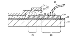
しかしながら、図1のように、化合物半導体の基板10上に形成されたAu層34(Au配線層)にバリア層72を介しAlパッド70を形成し、Alパッド70にAlワイヤ40を接続すると、後述するがAlとAuとの反応が生じてしまうことがわかった。
However, as shown in FIG. 1, when the
本発明は、上記課題に鑑みなされたものであり、Alパッド上にボンディングワイヤを形成することによる、AlパッドとAu配線層との反応を抑制することを目的とする。 The present invention has been made in view of the above problems, and an object of the present invention is to suppress a reaction between an Al pad and an Au wiring layer by forming a bonding wire on the Al pad.
本発明は、化合物半導体層上に設けられ、Alを含み、かつボンディング領域を避けて設けられた配線接続部を有するパッドと、前記パッドの前記配線接続部に電気的に接続されたAuを含む配線層と、前記配線接続部と前記配線層との間に設けられたバリア層と、前記配線層の端部において、前記配線層と前記パッドとの間に設けられた第1絶縁層と、を具備し、前記パッドの前記配線接続部上には、前記配線層および前記バリア層が延在し、前記パッドの前記ボンディング領域上には、前記配線層および前記バリア層が延在していないことを特徴とする半導体装置である。本発明によれば、パッドにボンディングワイヤが接続されるべきボンディング領域を避けて設けられた配線接続部において、配線層がバリア層を介しパッドに接続されている。これにより、ワイヤボンディングにより、パッドと配線層とが反応することを抑制できる。 The present invention includes a pad provided on a compound semiconductor layer, including Al and having a wiring connection portion provided to avoid a bonding region, and Au electrically connected to the wiring connection portion of the pad. A wiring layer, a barrier layer provided between the wiring connection portion and the wiring layer, and a first insulating layer provided between the wiring layer and the pad at an end of the wiring layer; And the wiring layer and the barrier layer extend on the wiring connection portion of the pad, and the wiring layer and the barrier layer do not extend on the bonding region of the pad. This is a semiconductor device. According to the present invention, the wiring layer is connected to the pad via the barrier layer in the wiring connection portion provided to avoid the bonding region where the bonding wire should be connected to the pad. Thereby, it can suppress that a pad and a wiring layer react by wire bonding.
上記構成において、前記半導体装置の使用上限温度は200℃以上である構成とすることができる。この構成によれば、AlとAuとが反応する温度である200℃以上においても、AlとAuとの反応を抑制することができる。 In the above structure, the upper limit use temperature of the semiconductor device may be 200 ° C. or higher. According to this configuration, the reaction between Al and Au can be suppressed even at 200 ° C. or higher, which is the temperature at which Al and Au react.
前記ボンディング領域に接続されるべきボンディングワイヤの太さは100μmφ以上である構成とすることができる。この構成によれば、ボンディングの際パッドに加わる圧力が大きい場合も、AlとAuとの反応を抑制することができる。 The thickness of the bonding wire to be connected to the bonding region may be 100 μmφ or more. According to this configuration, the reaction between Al and Au can be suppressed even when the pressure applied to the pad during bonding is large.
上記構成において、前記パッドの端部において、前記配線層と前記パッドとの間に設けられた第2絶縁層を具備する構成とすることができる。この構成によれば、パッドの端部におけるAuとAlが反応を抑制することができる。 The said structure WHEREIN: It can be set as the structure which comprises the 2nd insulating layer provided between the said wiring layer and the said pad in the edge part of the said pad. According to this structure, Au and Al in the edge part of a pad can suppress reaction.
上記構成において、前記パッドは第1層と該第1層上の第2層とからなり、前記配線層は前記第1層上に延在することにより前記パッドに接続され、前記ボンディング領域は前記第2層に設けられている構成とすることができる。この構成によれば、パッド端部のAlとAuとの反応を抑制し、かつボンディング領域に接続されるべきボンディングワイヤとパッドとの密着強度を保つことができる。 In the above configuration, the pad includes a first layer and a second layer on the first layer, the wiring layer is connected to the pad by extending on the first layer, and the bonding region is It can be set as the structure provided in the 2nd layer. According to this configuration, the reaction between Al and Au at the pad end can be suppressed, and the adhesion strength between the bonding wire and the pad to be connected to the bonding region can be maintained.
上記構成において、前記第2層は前記配線層上に第3絶縁層を介し延在する構成とすることができる。 The said structure WHEREIN: The said 2nd layer can be set as the structure extended through the 3rd insulating layer on the said wiring layer.
上記構成において、前記バリア層は、TiN、TiWN、WN、WSiN及びTaNのいずれかを含む構成とすることができる。 The said structure WHEREIN: The said barrier layer can be set as the structure containing either TiN, TiWN, WN, WSiN, and TaN.
上記構成において、前記バリア層の厚さは100nmから200nmである構成とすることができる。 In the above structure, the barrier layer may have a thickness of 100 nm to 200 nm.
上記構成において、前記ボンディングワイヤはAlを含む構成とすることができる。この構成によれば、ボンディングワイヤとパッドとの間での金属間反応を抑制することができる。 In the above configuration, the bonding wire may include Al. According to this structure, the intermetallic reaction between a bonding wire and a pad can be suppressed.
本発明によれば、パッドにボンディングワイヤが接続されるべきボンディング領域を避けて設けられた配線接続部において、配線層がバリア層を介しパッドに接続されている。これにより、ワイヤボンディングにより、パッドと配線層とが反応することを抑制できる。 According to the present invention, the wiring layer is connected to the pad via the barrier layer in the wiring connection portion provided to avoid the bonding region where the bonding wire should be connected to the pad. Thereby, it can suppress that a pad and a wiring layer react by wire bonding.
まず、図1に係る構造において、Alパッド70とAu層34とが反応する原因について調査した。その結果、Alワイヤ40をAlパッド70にワイヤボンディングした際に、バリア層72が破壊されることが原因であることがわかった。ワイヤボンディングする場合は、半導体チップに加える熱及び超音波並びにワイヤツールがパッドに加える圧力の寄与により、ボンディングワイヤとパッドとを機械的及び電気的に接続する。AuワイヤをAuパッドにボンディングする場合は、熱と超音波が主に寄与する(超音波熱圧着)。これに対しAlワイヤをAlパッドにボンディングする場合は、圧力が主に寄与する。このため、Alワイヤを用いる場合は、Auワイヤに比べ大きな圧力が必要となる。このため、特許文献1のような配線層上にバリア層を介しパッドが形成される構造では、バリア層が破壊されるものと考えられる。そこで、バリア層の破壊を抑制する実施例を以下に説明する。
First, the cause of the reaction between the
実施例1は、GaNを用いたFET(Field Effect Transistor)の例である。図2は実施例1に係る半導体装置内の半導体チップの平面図である。サファイア基板またはSiC(炭化シリコン)等の基板10上にGaNを含む半導体層であるGaN系半導体層が形成されている。GaN系半導体層上には、上からAl/Ti(チタン)からなるソース電極50及びドレイン電極52、上からAu/Ni(ニッケル)からなるゲート電極54が形成されている。ソース電極50、ドレイン電極52及びゲート電極54はフィンガを形成している。FET14は複数のフィンガで構成されている。すなわち、マルチフィンガ構造を有している。ソース電極50及びドレイン電極52上にはそれぞれ配線層30a及び30bが形成されている。配線層30a及び30bは櫛型をしており、フィンガがバスバーに接続されている。配線層30aのバスバーがAlパッド20a上に延在することにより、配線層30aとAlパッド20aとが電気的に接続されている。配線層30bとAlパッド20bにおいても同様である。各ゲート電極54はバスバー56を介しゲートパッド58に接続される。ゲートパッド58とAlパッド20cとは配線層30cを介し接続される。各配線層30aから30cは、バリア層とAu層とから構成される。各Alパッド20aから20cには、1または複数のAlワイヤ40が接続されている。
Example 1 is an example of an FET (Field Effect Transistor) using GaN. FIG. 2 is a plan view of the semiconductor chip in the semiconductor device according to the first embodiment. A GaN-based semiconductor layer, which is a semiconductor layer containing GaN, is formed on a
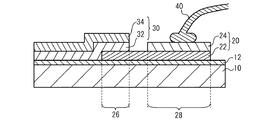
図3(a)及び図3(b)は基板10上に設けられたAlパッド20と配線層30とからなるパッド構造を示す平面図及び断面図である。図3(a)及び図3(b)を参照に、基板10上にGaN系半導体層である化合物半導体層12が設けられている。化合物半導体層12上にAlパッド20及び配線層30が形成されている。なお、化合物半導体層12上に層間絶縁膜や保護膜等の絶縁膜を介しAlパッド20及び配線層30が形成されていてもよい。また、Alパッド20及び配線層30の一部は、化合物半導体層12を介さず基板10上に設けられていてもよい。Alパッド20上に配線層30が延在することにより、配線層30とAlパッド20とが電気的に接続されている。
FIG. 3A and FIG. 3B are a plan view and a cross-sectional view showing a pad structure including an
Alパッド20は膜厚が例えば2μmである。Alパッド20上には太さが200μmから300μmのAlワイヤ40が接続されている。配線層30は、バリア層32とバリア層32上のAu層34(Auを含む配線層、Au配線層)とからなる。バリア層32は、例えば膜厚が50nmから300nm、好ましくは100から200nmのTiN(窒化チタン)やTiWN(窒化チタンタングステン)等である。バリア層32として、他にWN(窒化タングステン)、WSiN(窒化珪化タングステン)またはTaN(窒化タンタル)等を用いることもできる。バリア層32の膜厚が薄すぎると膜厚のばらつき等によりより薄い箇所が生じるためバリア性が小さくなってしまう。一方、膜厚が厚すぎると、バリア層32をエッチングする際のオーバーエッチング時間が長くなり、バリア層32下の下地(実施例1では化合物半導体層12)がエッチングされてしまう。また、処理時間も長くなってしまう。よって、バリア層32の膜厚は例えば50nmから300nmであり、好ましくは100nmから200nmである。Au層34の膜厚は例えば5μmから10μmである。
The
実施例1によれば、Alパッド20にAlワイヤ40が接続される領域外において、配線層30がAlパッド20に電気的に接続している。つまり、Alパッド20は、Alワイヤ40が接続すべき領域であるボンディング領域28と、Au層34が接続されている配線接続部26と、を有しており、配線接続部26はボンディング領域28を避けて設けられている。このように、Alワイヤ40をAlパッド20に接続しているため、Alワイヤ40とAlパッド20とでは金属間反応は生じない。また、Alパッド20と配線層30とは、Alワイヤ40が接続されるボンディング領域28以外で接続している。よって、図1の比較例のように、Alワイヤ40のボンディングにより、Alパッド70と配線層30とが反応することを抑制できる。このように、Alパッド20上にAlワイヤ40を形成することによる、Alパッド20と配線層30との反応を抑制することができる。
According to the first embodiment, the
また、バッド20の配線接続部26とAu層34(Au配線層)との間にバリア層32が設けられている。これにより、Alパッド20と配線層30とが接触している領域におけるAlパッド20と配線層30との反応を抑制することができる。バリア層32はTiN、TiWN等例示した材料以外にも、AlとAuとの反応を抑制する材料であればよい。また、バリア層32とAu層34との間またはバリア層42の下に密着層等の別の導電層が設けられていてもよい。
A
実施例1に係る半導体装置によれば、使用上限温度は200℃以上とすることができる。AlパッドとAuワイヤとの接合強度はパープルプレーグにより150℃〜200℃以上で劣化することが知られている。AuパッドにAlワイヤを接合した場合も同様であると考えられる。よって、半導体装置の使用上限温度が200℃以上の場合、実施例1のパッド構造が有効である。なお、半導体装置の使用上限温度は、半導体装置を動作させる際、信頼性を保証される温度であり半導体装置ごとに定められた温度である。 According to the semiconductor device according to the first embodiment, the use upper limit temperature can be set to 200 ° C. or higher. It is known that the bonding strength between the Al pad and the Au wire deteriorates at 150 ° C. to 200 ° C. or more due to purple plague. The same can be said when an Al wire is bonded to an Au pad. Therefore, when the upper limit temperature of use of the semiconductor device is 200 ° C. or higher, the pad structure of Example 1 is effective. Note that the upper limit temperature for use of the semiconductor device is a temperature at which reliability is ensured when the semiconductor device is operated, and is a temperature determined for each semiconductor device.
また、AlとAuとの接触部に不純物が存在するとAlとAuとによる金属間化合物の生成が加速すると考えられている。半導体チップを樹脂封止する場合、封止樹脂のガラス転位温度は一般的に150℃〜200℃である。ガラス転位温度を越えると封止樹脂の熱膨張係数が増加する。よって、150℃〜200℃以上では樹脂と半導体チップとの間に隙間が生じる。この隙間を介し侵入した酸素が封止樹脂を酸化し、酸化物の分解生成物がAlとAuの接合部に不純物として供給される。以上により、樹脂封止された半導体装置においては、使用上限温度が200℃以上の場合、特にAlとAuの反応が起こりやすい。よって、実施例1のパッド構造が特に有効である。 In addition, it is considered that the generation of an intermetallic compound by Al and Au is accelerated when impurities are present at the contact portion between Al and Au. When resin-sealing a semiconductor chip, the glass transition temperature of the sealing resin is generally 150 ° C. to 200 ° C. When the glass transition temperature is exceeded, the thermal expansion coefficient of the sealing resin increases. Accordingly, a gap is generated between the resin and the semiconductor chip at 150 ° C. to 200 ° C. or higher. Oxygen that has entered through this gap oxidizes the sealing resin, and oxide decomposition products are supplied as impurities to the joint between Al and Au. As described above, in a resin-encapsulated semiconductor device, when the upper limit temperature of use is 200 ° C. or higher, the reaction between Al and Au is particularly likely to occur. Therefore, the pad structure of Example 1 is particularly effective.
さらに、高電力用途の半導体装置においては、供給される電流量が大きく発熱量が大きいため、使用環境温度は実質的に200℃以上となる。よって、高電力用途の半導体装置の場合、実施例1に係る構成を用いることが好ましい。 Furthermore, in a semiconductor device for high power use, since the amount of current supplied is large and the amount of heat generated is large, the operating environment temperature is substantially 200 ° C. or higher. Therefore, in the case of a semiconductor device for high power use, it is preferable to use the configuration according to the first embodiment.
Alワイヤ40の太さは100μmφ以上であることが好ましい。高電力用途の半導体装置に用いられるAlワイヤは、大電流を流すため太線ワイヤとよばれ、100μmφ以上500μmφ以下の太さを有している。高出力用途の半導体装置以外に用いられるAlワイヤの太さは50μmφ以下であり、太線ワイヤとはその用途が異なっている。Alワイヤ40が太い場合は、ワイヤボンディングする際、Alパッド20に加わる圧力が大きくなる。よって、太線ワイヤを用いる場合バリア層32が破壊され易く、実施例1に係るパッド構造を用いることが好ましい。なお、例えば、太さ25μmφのAuワイヤをAuパッド上にボンディングする場合の荷重は0.5N程度であるが、太さ250μmφのAlワイヤをAlパッド上にボンディングする場合の荷重は5N程度である。このように、ワイヤの種類と太さが異なることにより1桁大きい圧力がパッドに加わる。
The thickness of the
コンバータ、インバータまたはスイッチングレギュレータのスイッチに用いる高出力用途の半導体装置は、印加される電圧の2.5倍の耐圧が要求される。よって、日本における100Vの交流に用いる場合は、耐圧は250V以上が求められる。さらに、各国に使用するため240Vの交流にも用いられる場合は、600V以上の耐圧が求められる。よって、高出力用途の半導体装置とは、例えば、耐圧が250V以上であり、好ましくは600V以上である。 A high-power semiconductor device used for a converter, inverter, or switching regulator switch is required to have a withstand voltage 2.5 times the applied voltage. Therefore, when used for 100V AC in Japan, the withstand voltage is required to be 250V or higher. Furthermore, when used in 240V AC for use in various countries, a withstand voltage of 600V or higher is required. Therefore, the semiconductor device for high output use has, for example, a withstand voltage of 250 V or more, and preferably 600 V or more.
高出力用途の半導体装置において求められる耐圧は、FETの場合はドレイン耐圧である。バイポーラトランジスタまたは(絶縁ゲートバイポーラトランジスタ)の場合はコレクタ耐圧である。 The breakdown voltage required for a semiconductor device for high output applications is the drain breakdown voltage in the case of an FET. In the case of a bipolar transistor or (insulated gate bipolar transistor), it is the collector breakdown voltage.
実施例1は、化合物半導体層12として、GaN系半導体層の例であったが、GaAs系半導体層であってもよい。GaAsを用いた半導体装置においても、Au配線層が一般的に用いられており、Alワイヤをワイヤボンディングする場合は、実施例1に係るパッド構造を適用することが好ましい。このように、化合物半導体層12はIII−V族化合物半導体層であることが好ましい。
In Example 1, the
GaN系半導体層を用いる場合、ソース電極50及びドレイン電極52は上からAl/Ta(タンタル)、Al/Pd(パラジウム)/Ta、またはMo(モリブデン)/Taを用いることができる。ゲート電極54としては、上から(Au、Cu(銅)またはAl)/TiWN、(Au、CuまたはAl)/(TiWNまたはPd)/(Ni、TiまたはIr(イリジウム))を用いることができる。化合物半導体層上に形成される電極は、特にこれらに限られないが、いずれかの電極がAuを含む場合、Au配線層を用いることが多い。よって、化合物半導体層上に形成された電極はAuを含むことが好ましい。
When a GaN-based semiconductor layer is used, the
図4は、実施例2のパッド構造を示す図である。図4を参照に、実施例2においては、Alパッド20上の配線層30の端部(ボンディング領域28と配線接続部26との間)において、配線層30がAlパッド20から離間している。その他の構成は実施例1の図3(b)と同じであり説明を省略する。実施例2のように、配線層30の端部において、配線層30はAlパッド20から離間していてもよい。
FIG. 4 is a diagram illustrating the pad structure of the second embodiment. With reference to FIG. 4, in Example 2, the
図5(a)及び図5(b)は、実施例3のパッド構造を示す図である。図5(a)及び図5(b)を参照に、実施例3においては、例えば酸化シリコンまたは窒化シリコンからなる第1絶縁層62が、Alパッド20上の配線層30の端部(ボンディング領域28と配線接続部26との間)において、配線層30とAlパッド20との間に設けられている。その他の構成は実施例1の図3(a)及び図3(b)と同じであり説明を省略する。実施例3によれば、Alパッド20上の配線層30の端部において、製造工程中にAuとAlとが接触することを抑制することができる。さらに、半導体装置の動作に伴うイオンマイグレーション等によりAuまたはAlがバリア層32表面を移動し、AuとAlとが反応することを抑制することができる。
FIGS. 5A and 5B are diagrams showing the pad structure of the third embodiment. Referring to FIGS. 5A and 5B, in Example 3, the first insulating
図6(a)及び図6(b)は、実施例4のパッド構造を示す図である。図6(a)及び図6(b)を参照に、実施例4においては、Alパッド20の端部において、配線層30とAlパッド20との間に第2絶縁層64が設けられている。その他の構成は実施例1の図3(a)及び図3(b)と同じであり説明を省略する。配線層30がAlパッド20上に乗り上げる段差においては、バリア層32の被覆性劣化等により、AuとAlが反応することが起こりうる。実施例4によれば、Alパッド20の端部におけるAuとAlが反応を抑制することができる。
FIG. 6A and FIG. 6B are diagrams showing the pad structure of the fourth embodiment. With reference to FIGS. 6A and 6B, in Example 4, the second insulating
図7(a)及び図7(b)は、実施例5のパッド構造を示す図である。図7(a)及び図7(b)を参照に、実施例5においては、絶縁層63が、実施例3の第1絶縁層と実施例4の第2絶縁層とを有し、環状をなしている。その他の構成は実施例1の図3(a)及び図3(b)と同じであり説明を省略する。実施例5によれば、Alパッド20上の配線層30の端部及びAlパッド20端部の配線層30の乗り上げ部分におけるAuとAlとの反応を抑制することができる。
FIG. 7A and FIG. 7B are diagrams showing the pad structure of the fifth embodiment. Referring to FIGS. 7A and 7B, in Example 5, the insulating
図8は、実施例6のパッド構造を示す図である。図8を参照に、実施例6においては、Alパッド20はAlからなる第1層22と第1層22上のAlからなる第2層24とからなる。配線層30は第1層22上に延在することによりAlパッド20に接続される。Alワイヤ40は第2層24上に接続されている。その他の構成は実施例1の図3(b)と同じであり説明を省略する。Alパッド20の膜厚はAlワイヤ40とAlパッド20との密着強度を保つため、2μm以上あることが好ましい。一方、Alパッド20の膜厚が大きいと、実施例4において説明したように、Alパッド20端部の配線層30の乗り上げ部分において、AuとAlとが反応しやすい。実施例6によれば、第1層22の膜厚を小さくすることにより、Alパッド20端部の配線層30の乗り上げ部分の段差を小さくすることができる。これにより、AlとAuとの反応を抑制することができる。一方、第2層24を厚くすることにより、Alワイヤ40とAlパッド20との密着強度を保つことができる。
FIG. 8 is a diagram illustrating the pad structure of the sixth embodiment. Referring to FIG. 8, in Example 6, the
図9(a)及び図9(b)は、実施例7のパッド構造を示す図である。図9(a)及び図9(b)を参照に、実施例7においては、第2層24が配線層30上に第3絶縁層66を介し延在している。その他の構成は実施例6の図8(a)及び図8(b)と同じであり、説明を省略する。実施例7によれば、配線層30の端部を第3絶縁層66及び第2層24が覆っているため、Alワイヤ40が配線層30に接触することを抑制することができる。
FIG. 9A and FIG. 9B are diagrams showing the pad structure of the seventh embodiment. With reference to FIGS. 9A and 9B, in Example 7, the
図10(a)及び図10(b)は、実施例8のパッド構造を示す図である。図10(a)及び図10(b)を参照に、実施例8においては、第1絶縁層62が、第1層22上の配線層30の端部において、配線層30と第1層22との間に設けられている。その他の構成は実施例7の図9(a)及び図9(b)と同じであり説明を省略する。実施例8によれば、第1絶縁層62により、第1層22上の配線層30の端部においてAuとAlが反応することを抑制することができる。また、第3絶縁層66及び第2層24によりAlワイヤ40が配線層30に接触することを抑制することができる。
FIG. 10A and FIG. 10B are diagrams showing the pad structure of the eighth embodiment. Referring to FIGS. 10A and 10B, in Example 8, the first insulating
図11は、実施例9のパッド構造を示す図である。図11を参照に、実施例9においては、Alパッド20は配線層30上に延在することにより配線層30と接続している。配線層30はAu層34上にバリア層32が形成されている。つまり、Au層34とAlパッド20との間にバリア層32が設けられている。その他の構成は実施例1の図3(b)と同じであり説明を省略する。
FIG. 11 is a diagram illustrating the pad structure of the ninth embodiment. Referring to FIG. 11, in Example 9, the
図12は、実施例10のパッド構造を示す図である。図12を参照に、実施例10においては、配線層30の端部において、配線層30とAlパッド20との間に第4絶縁層68が設けられている。その他の構成は実施例9の図11と同じであり説明を省略する。実施例10によれば、第4絶縁層68により、配線層30の端部におけるAlとAuの反応を抑制することができる。
FIG. 12 is a diagram illustrating the pad structure of the tenth embodiment. Referring to FIG. 12, in Example 10, a fourth insulating
GaNを用いたFETでは、ソース電極50及びドレイン電極52はAl/Ti等のAlを含む電極が一般的に用いられる。実施例1から実施例8によれば、このようなAlを含む電極を形成する際にAlパッド20を同時に形成することができる。また、Alを含む電極を用いない場合は、Alパッド20を形成した後に配線層30を形成してもよいが、実施例9及び実施例10のように、配線層30を形成した後にAlパッド20を形成することができる。このように、Alを含む電極を用いる場合及び、用いない場合のいずれの場合も、実施例1から実施例8並びに実施例9及び実施例10のいずれの構造も選択することができる。
In the FET using GaN, the
以上、発明の好ましい実施例について詳述したが、本発明は係る特定の実施例に限定されるものではなく、特許請求の範囲に記載された本発明の要旨の範囲内において、種々の変形・変更が可能である。 The preferred embodiments of the present invention have been described in detail above. However, the present invention is not limited to the specific embodiments, and various modifications and changes can be made within the scope of the gist of the present invention described in the claims. It can be changed.
10 基板
12 化合物半導体層
20 Alパッド
22 第1層
24 第2層
30 配線層
32 バリア層
34 Au層
40 Alワイヤ
62 第1絶縁層
63 絶縁層
64 第2絶縁層
66 第3絶縁層
68 第4絶縁層
DESCRIPTION OF
Claims (9)
前記パッドの前記配線接続部に電気的に接続されたAuを含む配線層と、
前記配線接続部と前記配線層との間に設けられたバリア層と、
前記配線層の端部において、前記配線層と前記パッドとの間に設けられた第1絶縁層と、
を具備し、
前記パッドの前記配線接続部上には、前記配線層および前記バリア層が延在し、前記パッドの前記ボンディング領域上には、前記配線層および前記バリア層が延在していないことを特徴とする半導体装置。 A pad provided on the compound semiconductor layer, including Al, and having a wiring connection portion provided avoiding the bonding region;
A wiring layer including Au electrically connected to the wiring connection portion of the pad;
A barrier layer provided between the wiring connection portion and the wiring layer;
A first insulating layer provided between the wiring layer and the pad at an end of the wiring layer;
Comprising
The wiring layer and the barrier layer extend on the wiring connection portion of the pad, and the wiring layer and the barrier layer do not extend on the bonding region of the pad. Semiconductor device.
前記配線層は前記第1層上に延在することにより前記パッドに接続され、
前記ボンディング領域は前記第2層に設けられていることを特徴とする請求項1記載の半導体装置。 The pad comprises a first layer and a second layer on the first layer;
The wiring layer is connected to the pad by extending on the first layer;
The semiconductor device according to claim 1, wherein the bonding region is provided in the second layer.
Priority Applications (2)
| Application Number | Priority Date | Filing Date | Title |
|---|---|---|---|
| JP2007075858A JP5192163B2 (en) | 2007-03-23 | 2007-03-23 | Semiconductor device |
| US12/054,087 US8222736B2 (en) | 2007-03-23 | 2008-03-24 | Semiconductor device with Al pad |
Applications Claiming Priority (1)
| Application Number | Priority Date | Filing Date | Title |
|---|---|---|---|
| JP2007075858A JP5192163B2 (en) | 2007-03-23 | 2007-03-23 | Semiconductor device |
Publications (3)
| Publication Number | Publication Date |
|---|---|
| JP2008235728A JP2008235728A (en) | 2008-10-02 |
| JP2008235728A5 JP2008235728A5 (en) | 2010-05-06 |
| JP5192163B2 true JP5192163B2 (en) | 2013-05-08 |
Family
ID=39773866
Family Applications (1)
| Application Number | Title | Priority Date | Filing Date |
|---|---|---|---|
| JP2007075858A Active JP5192163B2 (en) | 2007-03-23 | 2007-03-23 | Semiconductor device |
Country Status (2)
| Country | Link |
|---|---|
| US (1) | US8222736B2 (en) |
| JP (1) | JP5192163B2 (en) |
Families Citing this family (7)
| Publication number | Priority date | Publication date | Assignee | Title |
|---|---|---|---|---|
| JP4952534B2 (en) * | 2007-11-20 | 2012-06-13 | 三菱電機株式会社 | Manufacturing method of nitride semiconductor light emitting device |
| JP5468804B2 (en) * | 2009-03-31 | 2014-04-09 | 古河電気工業株式会社 | Semiconductor chip, semiconductor package, power module, and manufacturing method of semiconductor package |
| JP2011040582A (en) | 2009-08-11 | 2011-02-24 | Fuji Xerox Co Ltd | Light-emitting element, and method for manufacturing the same |
| US20140209926A1 (en) * | 2013-01-28 | 2014-07-31 | Win Semiconductors Corp. | Semiconductor integrated circuit |
| JP6211867B2 (en) * | 2013-09-24 | 2017-10-11 | ルネサスエレクトロニクス株式会社 | Semiconductor device |
| EP3182443B1 (en) * | 2014-08-11 | 2019-12-18 | Panasonic Intellectual Property Management Co., Ltd. | Semiconductor device |
| JP6738169B2 (en) * | 2016-03-11 | 2020-08-12 | Dowaエレクトロニクス株式会社 | Semiconductor optical device and manufacturing method thereof |
Family Cites Families (23)
| Publication number | Priority date | Publication date | Assignee | Title |
|---|---|---|---|---|
| US4388512A (en) * | 1981-03-09 | 1983-06-14 | Raytheon Company | Aluminum wire ball bonding apparatus and method |
| JPS59210656A (en) * | 1983-05-16 | 1984-11-29 | Fujitsu Ltd | Semiconductor device |
| JPS61220462A (en) * | 1985-03-27 | 1986-09-30 | Toshiba Corp | Compound semiconductor device |
| US4880708A (en) * | 1988-07-05 | 1989-11-14 | Motorola, Inc. | Metallization scheme providing adhesion and barrier properties |
| JPH0760839B2 (en) * | 1990-03-15 | 1995-06-28 | 株式会社東芝 | Semiconductor device |
| JPH04102358A (en) * | 1990-08-21 | 1992-04-03 | Ngk Spark Plug Co Ltd | Wiring board |
| DE69233801D1 (en) * | 1991-07-24 | 2011-02-17 | Denki Kagaku Kogyo Kk | A method of manufacturing a circuit substrate with a mounted semiconductor element |
| EP0646959B1 (en) * | 1993-09-30 | 2001-08-16 | Consorzio per la Ricerca sulla Microelettronica nel Mezzogiorno | Metallization and bonding process for manufacturing power semiconductor devices |
| JPH10189649A (en) * | 1996-12-20 | 1998-07-21 | Sharp Corp | Compound semiconductor device and method for forming electrode thereof |
| JP3379062B2 (en) | 1997-12-02 | 2003-02-17 | 富士通カンタムデバイス株式会社 | Semiconductor device and manufacturing method thereof |
| JP2000049184A (en) * | 1998-05-27 | 2000-02-18 | Hitachi Ltd | Semiconductor device and production thereof |
| US6427913B1 (en) * | 1998-09-11 | 2002-08-06 | Key-Trak, Inc. | Object control and tracking system with zonal transition detection |
| TW445616B (en) * | 1998-12-04 | 2001-07-11 | Koninkl Philips Electronics Nv | An integrated circuit device |
| US6511901B1 (en) * | 1999-11-05 | 2003-01-28 | Atmel Corporation | Metal redistribution layer having solderable pads and wire bondable pads |
| JP2002118121A (en) * | 2000-10-10 | 2002-04-19 | Sanyo Electric Co Ltd | Method for manufacturing compound semiconductor device |
| JP2002231748A (en) * | 2001-02-01 | 2002-08-16 | Sanyo Electric Co Ltd | Method for forming bump electrode |
| JP2003209134A (en) * | 2002-01-11 | 2003-07-25 | Hitachi Ltd | Semiconductor device and its manufacturing method |
| JP2005166946A (en) * | 2003-12-02 | 2005-06-23 | Espec Corp | Substrate and manufacturing method thereof |
| US7394161B2 (en) * | 2003-12-08 | 2008-07-01 | Megica Corporation | Chip structure with pads having bumps or wirebonded wires formed thereover or used to be tested thereto |
| DE112004003008T5 (en) * | 2004-10-29 | 2007-10-25 | Spansion Llc, Sunnyvale | Semiconductor device and method of making the same |
| JP4597653B2 (en) | 2004-12-16 | 2010-12-15 | 住友電工デバイス・イノベーション株式会社 | Semiconductor device, semiconductor module including the same, and method for manufacturing semiconductor device |
| JP2006245379A (en) * | 2005-03-04 | 2006-09-14 | Stanley Electric Co Ltd | Semiconductor light emitting device |
| US7361993B2 (en) * | 2005-05-09 | 2008-04-22 | International Business Machines Corporation | Terminal pad structures and methods of fabricating same |
-
2007
- 2007-03-23 JP JP2007075858A patent/JP5192163B2/en active Active
-
2008
- 2008-03-24 US US12/054,087 patent/US8222736B2/en active Active
Also Published As
| Publication number | Publication date |
|---|---|
| US20080230908A1 (en) | 2008-09-25 |
| US8222736B2 (en) | 2012-07-17 |
| JP2008235728A (en) | 2008-10-02 |
Similar Documents
| Publication | Publication Date | Title |
|---|---|---|
| JP5319084B2 (en) | Semiconductor device | |
| JP5192163B2 (en) | Semiconductor device | |
| TWI593110B (en) | Semiconductor device | |
| US9245845B2 (en) | Semiconductor device | |
| US10115798B2 (en) | Semiconductor device and method of manufacturing the same | |
| CN100495738C (en) | Integrated III-nitride power devices | |
| JP5433175B2 (en) | Semiconductor device | |
| US11456359B2 (en) | Semiconductor device and method of manufacturing semiconductor device | |
| JP6347309B2 (en) | Semiconductor device and manufacturing method of semiconductor device | |
| US20160155714A1 (en) | Semiconductor device, a power semiconductor device, and a method for processing a semiconductor device | |
| US9087833B2 (en) | Power semiconductor devices | |
| JP2009081198A (en) | Semiconductor device | |
| JP6066941B2 (en) | Semiconductor device | |
| JP4073876B2 (en) | Semiconductor device | |
| JP6545394B2 (en) | Semiconductor device | |
| US10418336B2 (en) | Manufacturing method of semiconductor device and semiconductor device | |
| JP6579653B2 (en) | Semiconductor device and manufacturing method of semiconductor device | |
| JP4977104B2 (en) | Diamond semiconductor element | |
| GB2535484B (en) | Wafer metallization of high power semiconductor devices | |
| CN110858610B (en) | Semiconductor device for electric power | |
| KR102106076B1 (en) | Power Semiconductor Device | |
| JP2022045568A (en) | Semiconductor device | |
| JPWO2020144790A1 (en) | Semiconductor devices for electric power | |
| CN117616566A (en) | Semiconductor device and method for manufacturing semiconductor device | |
| JP2008252115A (en) | Semiconductor device and manufacturing method thereof |
Legal Events
| Date | Code | Title | Description |
|---|---|---|---|
| A521 | Request for written amendment filed |
Free format text: JAPANESE INTERMEDIATE CODE: A523 Effective date: 20100319 |
|
| A621 | Written request for application examination |
Free format text: JAPANESE INTERMEDIATE CODE: A621 Effective date: 20100319 |
|
| A131 | Notification of reasons for refusal |
Free format text: JAPANESE INTERMEDIATE CODE: A131 Effective date: 20121016 |
|
| A977 | Report on retrieval |
Free format text: JAPANESE INTERMEDIATE CODE: A971007 Effective date: 20121018 |
|
| A521 | Request for written amendment filed |
Free format text: JAPANESE INTERMEDIATE CODE: A523 Effective date: 20121116 |
|
| TRDD | Decision of grant or rejection written | ||
| A01 | Written decision to grant a patent or to grant a registration (utility model) |
Free format text: JAPANESE INTERMEDIATE CODE: A01 Effective date: 20130129 |
|
| A61 | First payment of annual fees (during grant procedure) |
Free format text: JAPANESE INTERMEDIATE CODE: A61 Effective date: 20130131 |
|
| R150 | Certificate of patent or registration of utility model |
Ref document number: 5192163 Country of ref document: JP Free format text: JAPANESE INTERMEDIATE CODE: R150 Free format text: JAPANESE INTERMEDIATE CODE: R150 |
|
| FPAY | Renewal fee payment (event date is renewal date of database) |
Free format text: PAYMENT UNTIL: 20160208 Year of fee payment: 3 |
|
| R250 | Receipt of annual fees |
Free format text: JAPANESE INTERMEDIATE CODE: R250 |
|
| R250 | Receipt of annual fees |
Free format text: JAPANESE INTERMEDIATE CODE: R250 |