EP1391925B1 - Verfahren zur Selbstausrichtung einer damascenen Gatterstruktur zu Isolationsgebieten - Google Patents
Verfahren zur Selbstausrichtung einer damascenen Gatterstruktur zu Isolationsgebieten Download PDFInfo
- Publication number
- EP1391925B1 EP1391925B1 EP03368080A EP03368080A EP1391925B1 EP 1391925 B1 EP1391925 B1 EP 1391925B1 EP 03368080 A EP03368080 A EP 03368080A EP 03368080 A EP03368080 A EP 03368080A EP 1391925 B1 EP1391925 B1 EP 1391925B1
- Authority
- EP
- European Patent Office
- Prior art keywords
- doped source
- insulator
- drain regions
- layer
- regions
- Prior art date
- Legal status (The legal status is an assumption and is not a legal conclusion. Google has not performed a legal analysis and makes no representation as to the accuracy of the status listed.)
- Expired - Lifetime
Links
Images


Classifications
-
- H—ELECTRICITY
- H10—SEMICONDUCTOR DEVICES; ELECTRIC SOLID-STATE DEVICES NOT OTHERWISE PROVIDED FOR
- H10D—INORGANIC ELECTRIC SEMICONDUCTOR DEVICES
- H10D64/00—Electrodes of devices having potential barriers
- H10D64/01—Manufacture or treatment
- H10D64/013—Manufacture or treatment of electrodes having a conductor capacitively coupled to a semiconductor by an insulator
- H10D64/01302—Manufacture or treatment of electrodes having a conductor capacitively coupled to a semiconductor by an insulator the insulator being formed after the semiconductor body, the semiconductor being silicon
- H10D64/01332—Making the insulator
- H10D64/01336—Making the insulator on single crystalline silicon, e.g. chemical oxidation using a liquid
- H10D64/01342—Making the insulator on single crystalline silicon, e.g. chemical oxidation using a liquid by deposition, e.g. evaporation, ALD or laser deposition
-
- H—ELECTRICITY
- H10—SEMICONDUCTOR DEVICES; ELECTRIC SOLID-STATE DEVICES NOT OTHERWISE PROVIDED FOR
- H10D—INORGANIC ELECTRIC SEMICONDUCTOR DEVICES
- H10D30/00—Field-effect transistors [FET]
- H10D30/01—Manufacture or treatment
- H10D30/021—Manufacture or treatment of FETs having insulated gates [IGFET]
- H10D30/022—Manufacture or treatment of FETs having insulated gates [IGFET] having lightly-doped source or drain extensions selectively formed at the sides of the gates
-
- H—ELECTRICITY
- H10—SEMICONDUCTOR DEVICES; ELECTRIC SOLID-STATE DEVICES NOT OTHERWISE PROVIDED FOR
- H10D—INORGANIC ELECTRIC SEMICONDUCTOR DEVICES
- H10D30/00—Field-effect transistors [FET]
- H10D30/01—Manufacture or treatment
- H10D30/021—Manufacture or treatment of FETs having insulated gates [IGFET]
- H10D30/0223—Manufacture or treatment of FETs having insulated gates [IGFET] having source and drain regions or source and drain extensions self-aligned to sides of the gate
- H10D30/0227—Manufacture or treatment of FETs having insulated gates [IGFET] having source and drain regions or source and drain extensions self-aligned to sides of the gate having both lightly-doped source and drain extensions and source and drain regions self-aligned to the sides of the gate, e.g. lightly-doped drain [LDD] MOSFET or double-diffused drain [DDD] MOSFET
-
- H—ELECTRICITY
- H10—SEMICONDUCTOR DEVICES; ELECTRIC SOLID-STATE DEVICES NOT OTHERWISE PROVIDED FOR
- H10D—INORGANIC ELECTRIC SEMICONDUCTOR DEVICES
- H10D64/00—Electrodes of devices having potential barriers
- H10D64/01—Manufacture or treatment
- H10D64/017—Manufacture or treatment using dummy gates in processes wherein at least parts of the final gates are self-aligned to the dummy gates, i.e. replacement gate processes
-
- H—ELECTRICITY
- H10—SEMICONDUCTOR DEVICES; ELECTRIC SOLID-STATE DEVICES NOT OTHERWISE PROVIDED FOR
- H10D—INORGANIC ELECTRIC SEMICONDUCTOR DEVICES
- H10D64/00—Electrodes of devices having potential barriers
- H10D64/01—Manufacture or treatment
- H10D64/018—Spacers formed inside holes at the prospective gate locations, e.g. holes left by removing dummy gates
-
- H—ELECTRICITY
- H10—SEMICONDUCTOR DEVICES; ELECTRIC SOLID-STATE DEVICES NOT OTHERWISE PROVIDED FOR
- H10D—INORGANIC ELECTRIC SEMICONDUCTOR DEVICES
- H10D64/00—Electrodes of devices having potential barriers
- H10D64/60—Electrodes characterised by their materials
- H10D64/66—Electrodes having a conductor capacitively coupled to a semiconductor by an insulator, e.g. MIS electrodes
- H10D64/68—Electrodes having a conductor capacitively coupled to a semiconductor by an insulator, e.g. MIS electrodes characterised by the insulator, e.g. by the gate insulator
- H10D64/691—Electrodes having a conductor capacitively coupled to a semiconductor by an insulator, e.g. MIS electrodes characterised by the insulator, e.g. by the gate insulator comprising metallic compounds, e.g. metal oxides or metal silicates
-
- H—ELECTRICITY
- H10—SEMICONDUCTOR DEVICES; ELECTRIC SOLID-STATE DEVICES NOT OTHERWISE PROVIDED FOR
- H10D—INORGANIC ELECTRIC SEMICONDUCTOR DEVICES
- H10D84/00—Integrated devices formed in or on semiconductor substrates that comprise only semiconducting layers, e.g. on Si wafers or on GaAs-on-Si wafers
- H10D84/01—Manufacture or treatment
- H10D84/0123—Integrating together multiple components covered by H10D12/00 or H10D30/00, e.g. integrating multiple IGBTs
- H10D84/0126—Integrating together multiple components covered by H10D12/00 or H10D30/00, e.g. integrating multiple IGBTs the components including insulated gates, e.g. IGFETs
- H10D84/0165—Integrating together multiple components covered by H10D12/00 or H10D30/00, e.g. integrating multiple IGBTs the components including insulated gates, e.g. IGFETs the components including complementary IGFETs, e.g. CMOS devices
- H10D84/0188—Manufacturing their isolation regions
-
- H—ELECTRICITY
- H10—SEMICONDUCTOR DEVICES; ELECTRIC SOLID-STATE DEVICES NOT OTHERWISE PROVIDED FOR
- H10D—INORGANIC ELECTRIC SEMICONDUCTOR DEVICES
- H10D84/00—Integrated devices formed in or on semiconductor substrates that comprise only semiconducting layers, e.g. on Si wafers or on GaAs-on-Si wafers
- H10D84/01—Manufacture or treatment
- H10D84/02—Manufacture or treatment characterised by using material-based technologies
- H10D84/03—Manufacture or treatment characterised by using material-based technologies using Group IV technology, e.g. silicon technology or silicon-carbide [SiC] technology
- H10D84/038—Manufacture or treatment characterised by using material-based technologies using Group IV technology, e.g. silicon technology or silicon-carbide [SiC] technology using silicon technology, e.g. SiGe
-
- H—ELECTRICITY
- H10—SEMICONDUCTOR DEVICES; ELECTRIC SOLID-STATE DEVICES NOT OTHERWISE PROVIDED FOR
- H10W—GENERIC PACKAGES, INTERCONNECTIONS, CONNECTORS OR OTHER CONSTRUCTIONAL DETAILS OF DEVICES COVERED BY CLASS H10
- H10W10/00—Isolation regions in semiconductor bodies between components of integrated devices
- H10W10/01—Manufacture or treatment
- H10W10/011—Manufacture or treatment of isolation regions comprising dielectric materials
- H10W10/014—Manufacture or treatment of isolation regions comprising dielectric materials using trench refilling with dielectric materials, e.g. shallow trench isolations
- H10W10/0143—Manufacture or treatment of isolation regions comprising dielectric materials using trench refilling with dielectric materials, e.g. shallow trench isolations comprising concurrently refilling multiple trenches having different shapes or dimensions
-
- H—ELECTRICITY
- H10—SEMICONDUCTOR DEVICES; ELECTRIC SOLID-STATE DEVICES NOT OTHERWISE PROVIDED FOR
- H10W—GENERIC PACKAGES, INTERCONNECTIONS, CONNECTORS OR OTHER CONSTRUCTIONAL DETAILS OF DEVICES COVERED BY CLASS H10
- H10W10/00—Isolation regions in semiconductor bodies between components of integrated devices
- H10W10/10—Isolation regions comprising dielectric materials
- H10W10/17—Isolation regions comprising dielectric materials formed using trench refilling with dielectric materials, e.g. shallow trench isolations
-
- H—ELECTRICITY
- H10—SEMICONDUCTOR DEVICES; ELECTRIC SOLID-STATE DEVICES NOT OTHERWISE PROVIDED FOR
- H10D—INORGANIC ELECTRIC SEMICONDUCTOR DEVICES
- H10D64/00—Electrodes of devices having potential barriers
- H10D64/01—Manufacture or treatment
- H10D64/013—Manufacture or treatment of electrodes having a conductor capacitively coupled to a semiconductor by an insulator
- H10D64/01302—Manufacture or treatment of electrodes having a conductor capacitively coupled to a semiconductor by an insulator the insulator being formed after the semiconductor body, the semiconductor being silicon
- H10D64/01304—Manufacture or treatment of electrodes having a conductor capacitively coupled to a semiconductor by an insulator the insulator being formed after the semiconductor body, the semiconductor being silicon characterised by the conductor
- H10D64/01316—Manufacture or treatment of electrodes having a conductor capacitively coupled to a semiconductor by an insulator the insulator being formed after the semiconductor body, the semiconductor being silicon characterised by the conductor the conductor comprising a layer of elemental metal contacting the insulator, e.g. Ta, W, Mo or Al
-
- H—ELECTRICITY
- H10—SEMICONDUCTOR DEVICES; ELECTRIC SOLID-STATE DEVICES NOT OTHERWISE PROVIDED FOR
- H10D—INORGANIC ELECTRIC SEMICONDUCTOR DEVICES
- H10D64/00—Electrodes of devices having potential barriers
- H10D64/01—Manufacture or treatment
- H10D64/013—Manufacture or treatment of electrodes having a conductor capacitively coupled to a semiconductor by an insulator
- H10D64/01302—Manufacture or treatment of electrodes having a conductor capacitively coupled to a semiconductor by an insulator the insulator being formed after the semiconductor body, the semiconductor being silicon
- H10D64/01304—Manufacture or treatment of electrodes having a conductor capacitively coupled to a semiconductor by an insulator the insulator being formed after the semiconductor body, the semiconductor being silicon characterised by the conductor
- H10D64/01318—Manufacture or treatment of electrodes having a conductor capacitively coupled to a semiconductor by an insulator the insulator being formed after the semiconductor body, the semiconductor being silicon characterised by the conductor the conductor comprising a layer of alloy material, compound material or organic material contacting the insulator, e.g. TiN
- H10D64/0132—Manufacture or treatment of electrodes having a conductor capacitively coupled to a semiconductor by an insulator the insulator being formed after the semiconductor body, the semiconductor being silicon characterised by the conductor the conductor comprising a layer of alloy material, compound material or organic material contacting the insulator, e.g. TiN the conductor being a metallic silicide
-
- H—ELECTRICITY
- H10—SEMICONDUCTOR DEVICES; ELECTRIC SOLID-STATE DEVICES NOT OTHERWISE PROVIDED FOR
- H10D—INORGANIC ELECTRIC SEMICONDUCTOR DEVICES
- H10D64/00—Electrodes of devices having potential barriers
- H10D64/01—Manufacture or treatment
- H10D64/013—Manufacture or treatment of electrodes having a conductor capacitively coupled to a semiconductor by an insulator
- H10D64/01302—Manufacture or treatment of electrodes having a conductor capacitively coupled to a semiconductor by an insulator the insulator being formed after the semiconductor body, the semiconductor being silicon
- H10D64/01332—Making the insulator
- H10D64/01336—Making the insulator on single crystalline silicon, e.g. chemical oxidation using a liquid
-
- H—ELECTRICITY
- H10—SEMICONDUCTOR DEVICES; ELECTRIC SOLID-STATE DEVICES NOT OTHERWISE PROVIDED FOR
- H10D—INORGANIC ELECTRIC SEMICONDUCTOR DEVICES
- H10D64/00—Electrodes of devices having potential barriers
- H10D64/60—Electrodes characterised by their materials
- H10D64/66—Electrodes having a conductor capacitively coupled to a semiconductor by an insulator, e.g. MIS electrodes
- H10D64/665—Electrodes having a conductor capacitively coupled to a semiconductor by an insulator, e.g. MIS electrodes the conductor comprising a layer of elemental metal contacting the insulator, e.g. tungsten or molybdenum
-
- H—ELECTRICITY
- H10—SEMICONDUCTOR DEVICES; ELECTRIC SOLID-STATE DEVICES NOT OTHERWISE PROVIDED FOR
- H10D—INORGANIC ELECTRIC SEMICONDUCTOR DEVICES
- H10D64/00—Electrodes of devices having potential barriers
- H10D64/60—Electrodes characterised by their materials
- H10D64/66—Electrodes having a conductor capacitively coupled to a semiconductor by an insulator, e.g. MIS electrodes
- H10D64/667—Electrodes having a conductor capacitively coupled to a semiconductor by an insulator, e.g. MIS electrodes the conductor comprising a layer of alloy material, compound material or organic material contacting the insulator, e.g. TiN workfunction layers
- H10D64/668—Electrodes having a conductor capacitively coupled to a semiconductor by an insulator, e.g. MIS electrodes the conductor comprising a layer of alloy material, compound material or organic material contacting the insulator, e.g. TiN workfunction layers the layer being a silicide, e.g. TiSi2
-
- H—ELECTRICITY
- H10—SEMICONDUCTOR DEVICES; ELECTRIC SOLID-STATE DEVICES NOT OTHERWISE PROVIDED FOR
- H10D—INORGANIC ELECTRIC SEMICONDUCTOR DEVICES
- H10D64/00—Electrodes of devices having potential barriers
- H10D64/60—Electrodes characterised by their materials
- H10D64/66—Electrodes having a conductor capacitively coupled to a semiconductor by an insulator, e.g. MIS electrodes
- H10D64/68—Electrodes having a conductor capacitively coupled to a semiconductor by an insulator, e.g. MIS electrodes characterised by the insulator, e.g. by the gate insulator
Definitions
- the present invention relates to methods used to fabricate semiconductor devices, and more specifically to a method used to self - align a damascene type gate structure to isolation regions.
- Micro-miniaturization or the ability to fabricate semiconductor devices comprised with sub-micron features, has been directly related to advances in photolithography.
- the use of more sophisticated exposure cameras as well as the use of more advanced photosensitive materials have allowed the desired sub-micron images to be defined in photoresist layers.
- the same photoresist layers comprised with the sub-micron images are than used as an etch mask to allow the sub-micron images or features to be transferred to materials used for semiconductor device via anisotropic dry etching procedures.
- anisotropic dry etching procedures are used as an etch mask to allow the sub-micron images or features to be transferred to materials used for semiconductor device via anisotropic dry etching procedures.
- the ability to correctly align or overlay overlying sub-micron features to underlying sub-micron features can still present problems.
- the present invention will describe a novel process sequence in which a gate structure, and an underlying gate insulator layer, are formed, self-aligned to existing isolation regions.
- This novel process sequence employs only a single photolithographic procedure, and a single photolithographic mask or reticle, to form the isolation regions, the subsequent self-aligned gate insulator layer and the gate structure.
- the gate structure and underlying gate insulator layer can be formed via damascene procedures, with the gate insulator layer comprised of a high dielectric constant (high k) gate insulator layer.
- Prior arts such as: Ang et al, in
- a method of forming a gate structure and underlying gate insulator shape, self-aligned to isolation regions is described.
- Silicon nitride shapes are formed on the top surface of both P well and N well regions located in top portions of a semiconductor substrate.
- silicon oxide spacers are formed on the sides of the silicon nitride shapes, overlying portions of the heavily doped source/drain regions.
- Photolithographic and dry etching procedures are then employed to form shallow trench shapes in portions of the semiconductor substrate located between the silicon nitride shapes, which are lined with the silicon oxide spacers.
- shallow trench isolation STI
- bottom portions of the STI structures located in the P well and N well regions of the semiconductor substrate, while overlying top portions of the STI structures are located between the silicon nitride shapes.
- Selective removal of the silicon nitride shapes results in STI structures now comprised with, and widened by the addition of the remaining silicon oxide spacers.
- a high dielectric constant (high k) layer, and a conductive layer are deposited, followed by an etch back procedure resulting in a damascene type conductive gate structure and a high k gate insulator layer located between the silicon nitride spacers, which in turn are located on the sides of the exposed STI structures.
- Selective removal of the silicon nitride spacers allows the formation of lightly doped source/drain (LDD) regions, to be accomplished in the vacated space, with the LDD regions butting the heavily doped source/drain regions located under the STI regions.
- LDD lightly doped source/drain
- Refilling of the spaces created by removal of the silicon nitride spacers, with a silicon nitride - silicon oxide composite layer is followed by deposition of an interlevel dielectric (ILD) layer. Openings to the heavily doped source/drain regions in both P well and N well regions, are then accomplished in the ILD layer and in top portions of the STI structures, via selective dry etching procedures, using the silicon nitride component of the composite layer as a sidewall etch stop layer. Deposition of a metal layer, filling the openings, is followed by patterning procedures defining the desired metal contact and interconnect structures.
- ILD interlevel dielectric
- CMOS complimentary metal oxide semiconductor
- NMOS metal oxide semiconductor
- PMOS metal oxide semiconductor
- Semiconductor substrate 1 comprised of a P type, single crystalline silicon substrate, with a ⁇ 100> crystallographic orientation, is used and schematically shown in Fig. 1 .
- P well region 2 to be used to accommodate the NMOS device, is formed in a first region of semiconductor substrate 1.
- a photoresist shape (not shown in the drawings), is used as a block out mask, allowing implantation of boron or BF 2 ions to be performed in the first region of the semiconductor substrate, resulting in the formation of P well region 2.
- another photoresist block shape is used to mask P well region 2, from an implantation procedure used to form N well region 3, in a second region of semiconductor substrate 1. This is accomplished via implantation of arsenic or phosphorous ions.
- the photoresist block out shape is again removed via plasma oxygen ashing procedures.
- additional implantation procedures are performed to form punch through and threshold voltage adjust regions in top portions of both well regions. These regions are not shown in the drawings.
- a photoresist shape (not shown in the drawings), is next use as an etch mask to allow definition of the dummy mask gate shapes comprised of silicon nitride layer 5, on pad silicon oxide layer 4.
- the definition of the dummy gate mask shapes is accomplished via an anisotropic reactive ion etch (RIE), procedure, using CF 4 or Cl 2 as an etchant for silicon nitride, while using CHF 3 as a selective etchant for silicon oxide layer 4, with the RIE procedure selectively terminating with the appearance of the top surface of semiconductor substrate 1.
- RIE anisotropic reactive ion etch
- the photoresist shape used for definition of the dummy gate mask shapes is removed via plasma oxygen ashing.
- Photoresist shape 6 is next formed and used to protect N well region 3, located in the PMOS region of semiconductor substrate 1, from an implantation procedure used to define heavily doped N type source/drain regions 7, in P well region 2. This is accomplished using arsenic or phosphorous ions, implanted at an energy between about 1 to 100 KeV, at a dose between about 1E15 to 5E15 atoms/cm 2 . The result of this procedure is schematically shown in Fig. 4 . After removal of photoresist shape 6, via plasma oxygen ashing procedures, photoresist shape 8, is formed and used to block out the NMOS region of semiconductor substrate 1, from an implantation procedure used to form heavily doped P type source/drain regions 9, in N well region 3, located in the PMOS region of semiconductor substrate 1.
- a silicon oxide layer is next deposited to a thickness between about 50 to 1000 Angstroms, via LPCVD or PECVD procedures using tetraethylorthosilicate (TEOS), as a source. Narrow spaces between the dummy gate mask shapes located on both well regions are completely filled by the silicon oxide layer, while the wider spacers located between a dummy gate mask shape on a well region and a dummy gate mask shape located outside a well region, are not filled by the silicon oxide layer.
- TEOS tetraethylorthosilicate
- the result of these procedures is schematically shown in Fig. 6 .
- shallow trench shapes 11 is next addressed and schematically shown using Fig. 7 .
- a selective RIE procedure is employed to remove regions of semiconductor substrate 1, exposed in the wide spaces between dummy gate mask shapes, which are lined with silicon oxide spacers 10a.
- the selective RIE procedure is accomplished using SF 6 as the etchant for silicon, with a high etch rate ratio of silicon to either silicon nitride or silicon oxide, allowing shallow trench shapes 11, to be defined using silicon nitride of dummy gate mask shapes, and silicon oxide spacers 10a, as an etch mask.
- Silicon oxide shapes 10b located in the narrow spaces between dummy gate mask shapes, protected underlying well regions from this dry etch procedure.
- Shallow trench shapes 11, formed to a depth between about 1500 to 7000 Angstroms in semiconductor substrate 1, are located at the interface between P well region 2, and N well region 3, as well as at the interface between the well regions and the non-well regions of semiconductor substrate 1.
- Shallow trench shapes 11, are defined with a taper between about 75 to 90°, to optimize the filling of these shapes via subsequent CVD procedures.
- a thin liner silicon dioxide layer is thermally grown on the exposed surfaces of the shallow trench shapes.
- the liner layer not shown in the drawings, formed at a thickness between about 30 to 500 Angstroms, offers improved dielectric integrity when compared to a subsequent CVD silicon oxide layer used to completely fill the shallow trench shapes.
- Silicon oxide layer 12 is now deposited at a thickness between about 30 to 1000 Angstroms, via LPCVD or PECVD procedures using TEOS as a source, completely filling shallow trench shapes 11. Portions of silicon oxide layer 12, are also deposited overlying the top surface of silicon nitride layer 5, of dummy gate mask shapes, as well as overlying silicon oxide shapes 10b.
- CMP chemical mechanical polishing
- An anneal procedure is next performed at a temperature between about 500 to 1200° C, in an inert ambient, for purposes of densifying the chemically vapor deposited silicon oxide layer 12.
- the densification procedure results in the evolution STI regions 13a, now comprised of silicon oxide layer 12, in shallow trench shapes 11, and comprised of silicon oxide spacers 10a, previously located on the sides of dummy gate mask shapes.
- STI regions 13b are defined in the narrow spaces located between dummy gate mask shapes, with STI regions 13b, comprised with a bottom portion featuring silicon oxide shape 10b, and comprised with a top portion featuring silicon oxide layer 12.
- the result of the anneal procedure is schematically shown in Fig. 9 .
- Silicon nitride layer 5 is selectively removed via use of a hot phosphoric acid solution, exposing the top surface of pad silicon dioxide layer 4, located between the STI regions. If desired silicon nitride layer 5, can be removed via a RIE procedure using Cl 2 as a selective etchant for silicon nitride. Pad silicon dioxide layer 4, is next selectively removed via a RIE procedure using CHF 3 as an etchant. This procedure also results in some removal of silicon oxide from the top of the STI regions. All portions of the heavily doped source/drain regions, in both well regions, are entirely located underlying STI regions 13a, and STI regions 13b.
- a silicon nitride layer is next deposited at a thickness between about 30 to 1000 Angstroms, via LPCVD or PECVD procedures. The thickness of the silicon nitride layer will subsequently determine the width of lightly doped source/drain (LDD), regions.
- LDD lightly doped source/drain
- a high dielectric constant (high k), metal oxide layer such as aluminum oxide (Al 2 O 3 ), zirconium oxide (ZrO 2 ), or hafnium oxide (HfO 2 ), is next deposited at a thickness between about 15 to 300 Angstroms, via metal organic chemical vapor deposition (MOCVD), or via atomic layer chemical vapor deposition (ALCVD) procedures.
- High k layer 15 will be used as the gate insulator layer for the CMOS device.
- the high dielectric constant of high k metal oxide layer 15, between about 7 to 500, allows the use of a thicker layer.
- the higher dielectric constant layer allows an equivalent oxide thickness (EOT), equal to the thinner, lower k dielectric counterparts, to be realized.
- conductive layer comprised of a metal such as tungsten, aluminum, aluminum - copper, copper, or tungsten silicide, at a thickness between about 50 to 1000 Angstroms, via plasma vapor deposition (PVD), or via CVD procedures.
- the conductive layer can be comprised of an in situ doped polysilicon layer.
- the thickness of the conductive layer in the spaces between STI regions is greater than the thickness of the conductive layer on the top surface of the STI regions, thus a blanket etch back or chemical mechanical polishing (CMP), procedure can be used to form the desired conductive gate structure, self- aligned to STI regions without the use of photolithographic procedures.
- CMP chemical mechanical polishing
- etch back procedures used to remove thinner portions of conductive layer and of thinner high k layer from the top surface of all STI regions is accomplished using anisotropic RIE procedures, using Cl 2 as an etchant. This is schematically shown in Fig. 12 .
- a CMP procedure can also be used to remove the thinner portions of the conductive layer from the top surface of the STI regions, again resulting in definition of conductive gate structures, self-aligned to STI structures, with the definition of the conductive gate structures again accomplished without the use of photolithographic procedures.
- Silicon nitride spacers 14 are now selectively removed from the sides of STI regions 13a, and from the sides of STI regions 13b, via use of a hot phosphoric acid solution. If desired removal of silicon nitride spacers 14, can also be accomplished via a RIE procedure using Cl 2 or CF 4 as a selective etchant for silicon nitride. Spaces 17, created by the removal of silicon nitride spacers 14, exposing portions of P well region 2, and of N well region 3, will be subjected to ion implantation procedures used to form N type LDD regions 18, in exposed portions of P well region 2, and to form P type LDD regions 19, in N well region 3.
- N type LDD regions 18, are obtained via implantation of arsenic or phosphorous ions at an energy between about 1 to 100 KeV, at a dose between about 2E13 to 5E14 atoms/cm 2
- P type LDD regions 19 are obtained via implantation of boron or BF 2 ions, at an energy between about 0.1 to 30 KeV, at a dose between about 2E13 to 5E14 atoms/cm 2
- the LDD regions are formed self-aligned to conductive gate structures 16, butting heavily doped source/drain counterparts, located underlying the STI regions. The result of these procedures are schematically shown in Fig. 13 .
- Silicon oxide layer 20 is first deposited to a thickness between about 30 to 1000 Angstroms, via LPCVD or PECVD procedures. Silicon oxide layer 20, lines the sides of conductive gate structures 16, as well as the sides of STI regions 13a and 13b, however without completely filling spaces 17. Next silicon nitride layer 21, is deposited at a thickness between about 50 to 1000 Angstroms, via LPCVD or PECVD procedures, with the composite of silicon nitride layer 21, and silicon oxide layer 20, now completely filling spaces 19.
- a photoresist shape is then used as an etch mask to allow the portions of silicon nitride layer 21, to be removed from the top surfaces of STI regions 13a, and 13b, leaving the composite insulator layer, comprised of silicon nitride layer 21, and silicon oxide layer 20, only overlying conductive gate structures 16, as well as only filling spaces 19.
- the etch procedure used to accomplish this is a RIE procedure, employing CF 4 or Cl 2 as a selective etchant for silicon nitride.
- the photoresist shape used protect specific regions during the silicon nitride removal procedure, is then removed via plasma oxygen ashing procedures. If desired a CMP procedure can be used to remove the portions of silicon nitride layer 21, from the top surface of the STI regions, while other portions of silicon nitride layer 21, located on the shorter conductive gate structures, are left remaining.
- a CMP procedure is used for planarization purposes, resulting in a smooth top surface topography for ILD layer 22.
- a photoresist shape is used as an etch mask to allow openings 23, to be defined in ILD layer 22, as well as in portions of STI regions 13a, and 13b, exposing portions of the top surfaces of the heavily doped source/drain regions in both P well region 2, and N well region 3.
- Openings 23, are formed via a RIE procedure using CHF 3 as a selective etchant for silicon oxide or BPSG, therefore openings 23, butt silicon nitride component 21, of the composite insulator fill located in spaces 17.
- the presence of silicon nitride component 21, offers protection to the conductive gate structure and to the underlying high k gate insulator layer, during definition of openings 23, as well as during subsequent metal silicide formation procedures.
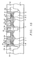
- the result of the above procedures is schematically shown in Fig. 15 .
- a metal layer such as cobalt, nickel, titanium, or tantalum, is deposited via PVD procedures, to a thickness between about 30 to 1000 Angstroms.
- An anneal procedure is performed using either conventional furnace procedures, or via use of rapid thermal anneal (RTA), procedures, resulting in formation of metal silicide on portions of the heavily doped source/drain regions exposed in openings 23.
- RTA rapid thermal anneal
- the metal silicide layers are not shown in the drawings. Portions of the metal layer located on the top surface of ILD layer 22, or on the inside walls of openings 22, remain unreacted and are selectively removed via wet etch procedures.
- a metal layer such as tungsten is next deposited via PVD or CVD procedures, at a thickness between about 500 to 5000 Angstroms, completely filling openings 22. Portions of the metal layer are then removed from the top surface of ILD layer 22, via a CMP procedure, resulting in formation of metal contact and interconnect structures 24, in openings 23, overlying and contacting N type heavily doped source/drain regions 7, located in P well region 2, of the NMOS device, and overlying and contacting P type heavily doped source/drain regions 9, located in N well region 3, of the PMOS device.
Landscapes
- Insulated Gate Type Field-Effect Transistor (AREA)
- Metal-Oxide And Bipolar Metal-Oxide Semiconductor Integrated Circuits (AREA)
- Electrodes Of Semiconductors (AREA)
- Element Separation (AREA)
- Drying Of Semiconductors (AREA)
Claims (23)
- Verfahren zum Herstellen eines Metalloxid-Halbleiter-Feldeffekttransistors (MOSFET)/Vorrichtung auf einem Halbleitersubstrat, umfassend die Schritte:- Bilden von zusammengesetzten lsolatorstrukturen (4, 5) auf oberen Flächen von ersten Abschnitten des Halbleitersubstrats (1);- Bilden von schwer dotierten Quellen/Senken-Bereichen (7) in zweiten Abschnitten des Halbleitersubstrat, die nicht durch die zusammengesetzten Isolatorstrukturen bedeckt sind;- Bilden von ersten Isolatorabstandstücken (10a) an Seiten der zusammengesetzten Isolatorstrukturen, wobei jedes erste Isolatorabstandstück einen Abschnitt eines schwer dotierten Quellen/Senken-Bereichs überdeckt und bedeckt;- Bestimmen von flachen Grabenöffnungen (11) in Abschnitten des Halbleitersubstrats, die nicht durch die zusammengesetzten lsolatorstrukturen oder durch die ersten lsolatorabstandstücke bedeckt sind;- Füllen der flachen Grabenöffnungen und Räume zwischen den zusammengesetzten Isolatorstrukturen mit einer ersten lsolatorschicht (12), was zu Bereichen von flacher Grabenisolation (STI) führt, wobei jeder STI-Bereich aus einer darunter liegenden, mit einem lsolator gefüllten flachen Grabenöffnung und aus einer darüber liegenden ersten Isolatorform (13a) besteht, die zwischen den zusammengesetzten Isolatorstrukturen angeordnet ist, wobei die ersten lsolatorabstandstücke an Seiten der zusammengesetzten lsolatorstrukturen angeordnet sind, nun ein Bestandteil der darüber liegenden ersten Isolatorform;- selektives Entfernen der zusammengesetzten Isolatorstrukturen;- Bilden von zweiten Isolatorabstandstücken (14) an Seiten der STI-Bereiche;- Bilden einer Gate-Isolatorschicht (15) an einem Abschnitt des Halbleitersubstrats, das nicht durch die STI-Bereiche oder die zweiten Isolatorabstandstücke bedeckt ist;- Bilden einer leitenden Gate-Struktur (16) an der Gate-Isolatorschicht, wobei die leitende Gate-Struktur sich selbst zu den STI-Bereichen ausrichtet;- Entfernen der zweiten lsolatorabstandstücke;- Bilden von leicht dotierten Quellen/Senken-Bereichen (18, 19) in Abschnitten des Halbleitersubstrats, die durch Entfernung der zweiten lsolatorabstandsstücke aufgedeckt werden, wobei jeder leicht dotierte Quellen/Senken-Bereich angrenzend zu und anstoßend an einen schwer dotierten Quellen/Senken-Bereich angeordnet ist, wobei dieser wiederum unter einem STI-Bereich angeordnet ist;- Bilden einer zusammengesetzten lsolatorschicht (20, 21) im Raum zwischen dem STI-Bereich und der leitenden Gate-Struktur, wobei die zusammengesetzte lsolatorschicht über dem leicht dotierten Quellen/Senken-Bereich angeordnet ist;- Ablagern einer zweiten lsolatorschicht (22);- Bilden von Öffnungen (23) in der zweiten Isolatorschicht und in den STI-Bereichen, um Abschnitte der schwer dotierten Quellen/Senken-Bereiche offenzulegen;- Bilden von Metallsilicid-Schichten an offengelegten Abschnitten des schwer dotierten Quellen/Senken-Bereichs; und- Bilden von Metallstrukturen (24) in den Öffnungen, wobei die Metallstrukturen über den Metallsilicid-Schichten angeordnet sind.
- Verfahren nach Anspruch 1, bei dem die zusammengesetzten Isolatorstrukturen aus einer darüber liegenden Silikon-Nitrid-Form mit einer Dicke zwischen ungefähr 50 bis 2.000 Angström (5 bis 200 nm) und aus einer darunter liegenden Silikon-Dioxid-Form bei einer Dicke zwischen ungefähr 30 bis 1.000 Angström (3 bis 100 nm) gebildet werden.
- Verfahren nach Anspruch 1, bei dem die schwer dotierten Quellen/Senken-Bereiche schwer dotierte Quellen/Senkenbereich vom N-Typ sind, die durch Implantation von Arsen- oder Phosphorionen erhalten werden, die bei einer Energie zwischen ungefähr 1 bis 100 KeV implantiert werden, bei einer Dosis zwischen ungefähr 1E15 bis 5E15 Atome/cm2.
- Verfahren nach Anspruch 1, bei dem die schwer dotierten Quellen/Senken-Bereiche schwer dotierte Quellen/Senken-Bereiche vom P-Typ sind, die durch Implantation von Bor- oder BF2-lonen erhalten werden, die bei einer Energie zwischen ungefähr 0,1 bis 30 KeV implantiert werden, bei einer Dosis zwischen ungefähr 1E15 bis 5E15 Atome/cm2.
- Verfahren nach Anspruch 1, bei dem die ersten lsolatorabstandsstücke Silikonoxid-Abstandsstücke sind, die durch Ablagerung einer Silikonoxidschicht mittels LPCVD- oder PECVD-Verfahren bei einer Dicke zwischen ungefähr 50 bis 1.000 Angström (5 bis 100 nm) erhalten werden, und dann mittels anisotroper RIE-Verfahren unter Verwendung von CHF3 als ein Ätzmittel bestimmt werden.
- Verfahren nach Anspruch 1, bei dem die erste lsolatorschicht, welche verwendet wird, um die flachen Grabenöffnungen zu füllen, eine Silikonoxid-Schicht ist, die durch LPCVD- oder PECVD-Verfahren bei einer Dicke zwischen ungefähr 30 bis 500 Angström (3 bis 50 nm) unter Verwendung von Tetraethylorthosilikat (TEOS) als eine Quelle erhalten werden.
- Verfahren nach Anspruch 1, bei dem die zweiten Isolatorabstandsstücke Silikonnitrid-AbstandsstÜcke sind, die durch Ablagerung einer Silikonnitrid-Schicht bei einer Dicke zwischen ungefähr 30 bis 1.000 Angström (3 bis 100 nm) mittels LPCVD- oder PECVD-Vefahren erhalten und dann mittels anisotropischer RIE-Verfahren unter Verwendung von CF4 oder Cl2 als ein Ätzmittel bestimmt werden.
- Verfahren nach Anspruch 1, bei dem die Gate-Isolatorschicht eine dielektrische Schicht mit hohem k ist, bestehend aus entweder Aluminiumoxid (Al2O3), Zirkoniumoxid (ZrO2) oder Hafniumoxid (HfO2),die bei einer Dicke zwischen ungefähr 15 bis 300 Angström (1,5 bis 30 nm) mittels Metall-organischer-chemischer Dampfablagerung (MOCVD) oder mittels Atomschicht-chemische Dampfablagerung (LCVD)-Verfahren erhalten werden.
- Verfahren nach Anspruch 1, bei dem die Gate-Isolatorschicht mit einer dielektrischen Konstanten zwischen ungefähr 7 bis 100 versehen ist.
- Verfahren nach Anspruch 1, bei dem die zweiten Isolatorabstandsstücke selektiv mittels Naßätzverfahren entfernt werden, unter Verwendung von heißer Phosphorsäure als ein Ätzmittel für Silikonnitrid.
- Verfahren nach Anspruch 1, bei dem die leicht dotierten Quellen/Senken-Bereiche schwer dotierte Quellen/Senken-Bereiche vom N-Typ sind, die mittels lmplantation von Arsen- oder Phosphorionen bei einer Energie zwischen ungefähr 1 bis 100 KeV implantiert werden, bei einer Dosis zwischen ungefähr 2E13 bis 5E14 Atomen/cm2.
- Verfahren nach Anspruch 1, bei dem die leicht dotierten Quellen/Senken-Bereiche schwer dotierte Quellen/Senken-Bereiche vom P-Typ sind, die mittels Implantation von Bor- oder BF2-lonen implantiert werden, bei einer Dosis zwischen ungefähr 2E13 bis 5E14 Atome/cm2.
- Verfahren nach Anspruch 1, bei dem die zusammengesetzte Isolatorschicht, die in dem Raum zwischen dem STI-Bereich und der leitenden Gate-Struktur angeordnet ist, eine darunter liegende Silikonoxid-Schicht, die bei einer Dicke zwischen ungefähr 30 bis 1.000 Angström (3 bis 100 nm) mittels LPCVD oder PECVD-Verfahren erhalten wird, und eine darüber liegende Silikonnitrid-Schicht umfasst, die bei einer Dicke zwischen ungefähr 50 bis 1.000 Angström (5 bis 100 nm) mittels LPCVD oder PECVD-Verfahren erhalten wird.
- Verfahren nach Anspruch 1, des weiteren umfassend:- Bilden eines P-Mulden-Bereiches in einem dritten Abschnitt des Halbleitersubstrat, der verwendet wird, um einen N-Kanal-Metalloxid-Halbleiter (NMOS) aufzunehmen, einer Vorrichtung der CMOS-Vorrichtung; und- Bilden eines N-Mulden-Bereiches in einem vierten Abschnitt des Halbleitersubstrat, das verwendet wird, um einen P-Kanal-Metalloxid-Halbleiter (PMOS) aufzunehmen, einer Vorrichtung der CMOS-Vorrichtung; wobei- die zusammengesetzten lsolatorstrukturen an der oberen Fläche des Halbleitersubstrats gebildet sind, die über den ersten Abschnitten sowohl des P-Mulden-Bereiches und des N-Mulden-Bereiches liegt, wobei jede der zusammengesetzten Isolatorstrukturen eine darüber liegende Silikonnitridform und eine darunter liegende Silikondioxidform umfasst;- wobei die schwer dotierten Quellen/Senken-Bereiche vom N-Typ in den zweiten Abschnitten des P-Mulden-Bereichs und des N-Mulden-Bereichs gebildet sind, die nicht von den zusammengesetzten lsolatorstrukturen bedeckt sind;- wobei die schwer dotierten Quellen/Senken-Bereiche vom N-Typ in den zweiten Abschnitten des P-Mulden-Bereiches gebildet sind, und wobei die schwer dotierten Quellen/Senken-Bereiche vom P-Typ in den zweiten Abschnitten des N-Mulden-Bereichs gebildet sind; und- wobei die leicht dotierten Quellen/Senken-Bereiche leicht dotierte Quellen/Senken-Bereiche vom N-Typ in Abschnitten des P-Mulden-Bereiches umfassen, der angrenzend und anstoßend an den schwer dotierten Quellen/Senken-Bereich vom N-Typ angeordnet ist.
- Verfahren nach Anspruch 1, bei dem die Metallsilicidschichten Kobaltsilicid umfassen.
- Verfahren nach Anspruch 14, bei dem die schwer dotierten Quellen/Senken-Bereiche vom N-Typ mittels lmplantation von Arsen- oder Phosphorionen erhalten werden, die bei einer Energie zwischen ungefähr 1 bis 100 KeV implantiert werden, bei einer Dosis zwischen 1E15 bis 5E15 Atome/cm2.
- Verfahren nach Anspruch 14, bei dem die schwer dotierten Quellen/Senken-Bereiche vom P-Typ mittels Implantation von Bor- oder BF2-lonen erhalten werden, die bei einer Energie zwischen ungefähr 0,1 bis 30 KeV implantiert werden, bei einer Dosis zwischen ungefähr 1E15 bis 5E15 Atome/cm2.
- Verfahren nach Anspruch 1, bei dem die flachen Grabenöffnungen bei einer Tiefe zwischen ungefähr 1.500 bis 7.000 Angström (150 bis 700 nm) in dem Halbleitersubstrat gebildet werden, mit einer Abschrägung zwischen ungefähr 75° bis 90° mittels eines RIE-Verfahrens unter Verwendung von SF6 als ein selektives Ätzmittel für Silikon.
- Verfahren nach Anspruch 1, bei dem die zusammengesetzten Isolatorabstandstücke mittels RIE-Verfahren unter Verwendung von CF4 oder Cl2 als ein Ätzmittel für Silikonnitrid entfernt werden, während CHF3 als ein Ätzmittel für Silikondioxid verwendet wird.
- Verfahren nach Anspruch 1, bei dem die Silikonnitridformen der zusammengesetzten lsolatorabstandsstücke selektiv mittels Naßätzverfahren unter Verwendung von heißer Phosphorsäurenlösung entfernt werden.
- Verfahren nach Anspruch 1, bei dem die leitende Gate-Struktur bei einer Dicke zwischen ungefähr 50 bis 1.000 Angström (5 bis 100 nm) gebildet wird und ein Material umfasst, das ausgewählt wird aus der Gruppe, die folgendes beinhaltet, Aluminium, Aluminiumkupfer, Kupfer, Wolfram, Wolframsilicid oder dotiertes Polysilikon,
- Verfahren nach Anspruch 14, bei dem die leicht dotierten Quellen/Senken-Bereiche vom N-Typ mittels Implantation von Arsen- oder Phosphorionen bei einer Energie zwischen ungefähr 1 bis 100 KeV implantiert werden, bei einer Dosis zwischen ungefähr 2E13 bis 5E14 Atome/cm2.
- Verfahren nach Anspruch 14, bei dem die leicht dotierten Quellen/Senken-Bereiche vom P-Typ mittels Implantation von Bor- oder BF2-lonen erhalten werden, die bei einer Dosis zwischen ungefähr 2E13 bis 5E14 Atome/cm2 implantiert werden.
Applications Claiming Priority (2)
| Application Number | Priority Date | Filing Date | Title |
|---|---|---|---|
| US225805 | 2002-08-22 | ||
| US10/225,805 US6713335B2 (en) | 2002-08-22 | 2002-08-22 | Method of self-aligning a damascene gate structure to isolation regions |
Publications (3)
| Publication Number | Publication Date |
|---|---|
| EP1391925A2 EP1391925A2 (de) | 2004-02-25 |
| EP1391925A3 EP1391925A3 (de) | 2005-04-20 |
| EP1391925B1 true EP1391925B1 (de) | 2008-07-16 |
Family
ID=31187999
Family Applications (1)
| Application Number | Title | Priority Date | Filing Date |
|---|---|---|---|
| EP03368080A Expired - Lifetime EP1391925B1 (de) | 2002-08-22 | 2003-08-20 | Verfahren zur Selbstausrichtung einer damascenen Gatterstruktur zu Isolationsgebieten |
Country Status (7)
| Country | Link |
|---|---|
| US (1) | US6713335B2 (de) |
| EP (1) | EP1391925B1 (de) |
| JP (1) | JP2004134757A (de) |
| AT (1) | ATE401665T1 (de) |
| DE (1) | DE60322154D1 (de) |
| SG (1) | SG102720A1 (de) |
| TW (1) | TWI260732B (de) |
Cited By (1)
| Publication number | Priority date | Publication date | Assignee | Title |
|---|---|---|---|---|
| US10283588B2 (en) | 2015-05-29 | 2019-05-07 | Stmicroelectronics (Crolles 2) Sas | Method for local isolation between transistors produced on an SOI substrate, in particular an FDSOI substrate, and corresponding integrated circuit |
Families Citing this family (20)
| Publication number | Priority date | Publication date | Assignee | Title |
|---|---|---|---|---|
| TW200425298A (en) * | 2003-05-01 | 2004-11-16 | Nanya Technology Corp | Fabrication method for a damascene bitline contact |
| US20050196946A1 (en) * | 2004-03-02 | 2005-09-08 | Matsushita Electric Industrial Co., Ltd. | Method for manufacturing solid-state imaging device |
| JP4577680B2 (ja) * | 2004-04-13 | 2010-11-10 | エルピーダメモリ株式会社 | 半導体装置の製造方法 |
| JP4054321B2 (ja) * | 2004-06-23 | 2008-02-27 | 松下電器産業株式会社 | 半導体装置 |
| US7118952B2 (en) * | 2004-07-14 | 2006-10-10 | Taiwan Semiconductor Manufacturing Co., Ltd. | Method of making transistor with strained source/drain |
| US7148548B2 (en) * | 2004-07-20 | 2006-12-12 | Intel Corporation | Semiconductor device with a high-k gate dielectric and a metal gate electrode |
| US7138323B2 (en) * | 2004-07-28 | 2006-11-21 | Intel Corporation | Planarizing a semiconductor structure to form replacement metal gates |
| KR100641993B1 (ko) * | 2004-12-15 | 2006-11-02 | 동부일렉트로닉스 주식회사 | 고유전율의 절연막을 갖는 씨모스 이미지 센서의 제조 방법 |
| CN101449270B (zh) * | 2006-03-15 | 2011-11-16 | 谷歌公司 | 自动显示尺寸调整后的图像 |
| TWI336918B (en) * | 2007-05-08 | 2011-02-01 | Nanya Technology Corp | Method of manufacturing the shallow trench isolation structure |
| US7998832B2 (en) * | 2008-08-27 | 2011-08-16 | Advanced Micro Devices, Inc. | Semiconductor device with isolation trench liner, and related fabrication methods |
| US8735991B2 (en) * | 2011-12-01 | 2014-05-27 | Taiwan Semiconductor Manufacturing Company, Ltd. | High gate density devices and methods |
| US9865690B2 (en) * | 2012-04-10 | 2018-01-09 | Qorvo Us, Inc. | Methods for fabricating a metal structure for a semiconductor device |
| US9165838B2 (en) * | 2014-02-26 | 2015-10-20 | Taiwan Semiconductor Manufacturing Company Limited | Methods of forming low resistance contacts |
| US9530853B2 (en) | 2014-03-10 | 2016-12-27 | Qorvo Us, Inc. | Semiconductor device with reduced leakage current and method for making the same |
| DE102014107994A1 (de) * | 2014-06-05 | 2015-12-17 | Infineon Technologies Austria Ag | Halbleitervorrichtung und Verfahren zum Herstellen der Halbleitervorrichtung |
| US9666586B2 (en) * | 2014-08-14 | 2017-05-30 | Gil Asa | CMOS compatible memory cells |
| US9378968B2 (en) * | 2014-09-02 | 2016-06-28 | United Microelectronics Corporation | Method for planarizing semiconductor device |
| US10147719B2 (en) * | 2016-11-17 | 2018-12-04 | Taiwan Semiconductor Manufacturing Co., Ltd. | Semiconductor field effect transistors and manufacturing method thereof |
| US10784359B2 (en) | 2018-05-18 | 2020-09-22 | Taiwan Semiconductor Manufacturing Company, Ltd. | Non-conformal oxide liner and manufacturing methods thereof |
Family Cites Families (8)
| Publication number | Priority date | Publication date | Assignee | Title |
|---|---|---|---|---|
| JPH1070187A (ja) | 1996-08-28 | 1998-03-10 | Mitsubishi Electric Corp | 半導体装置およびその製造方法 |
| JP4160167B2 (ja) * | 1997-06-30 | 2008-10-01 | 株式会社東芝 | 半導体装置の製造方法 |
| US6261887B1 (en) | 1997-08-28 | 2001-07-17 | Texas Instruments Incorporated | Transistors with independently formed gate structures and method |
| US6248643B1 (en) | 1999-04-02 | 2001-06-19 | Vanguard International Semiconductor Corporation | Method of fabricating a self-aligned contact |
| US6258677B1 (en) | 1999-10-01 | 2001-07-10 | Chartered Seminconductor Manufacturing Ltd. | Method of fabricating wedge isolation transistors |
| JP3538108B2 (ja) * | 2000-03-14 | 2004-06-14 | 松下電器産業株式会社 | 半導体装置及びその製造方法 |
| JP2001267561A (ja) * | 2000-03-21 | 2001-09-28 | Sony Corp | 半導体装置の製造方法及び半導体装置 |
| US6204137B1 (en) * | 2000-04-24 | 2001-03-20 | Chartered Semiconductor Manufacturing, Ltd. | Method to form transistors and local interconnects using a silicon nitride dummy gate technique |
-
2002
- 2002-08-22 US US10/225,805 patent/US6713335B2/en not_active Expired - Fee Related
-
2003
- 2003-08-05 SG SG200304568A patent/SG102720A1/en unknown
- 2003-08-05 TW TW092121331A patent/TWI260732B/zh active
- 2003-08-20 EP EP03368080A patent/EP1391925B1/de not_active Expired - Lifetime
- 2003-08-20 DE DE60322154T patent/DE60322154D1/de not_active Expired - Lifetime
- 2003-08-20 AT AT03368080T patent/ATE401665T1/de not_active IP Right Cessation
- 2003-08-21 JP JP2003297152A patent/JP2004134757A/ja active Pending
Cited By (1)
| Publication number | Priority date | Publication date | Assignee | Title |
|---|---|---|---|---|
| US10283588B2 (en) | 2015-05-29 | 2019-05-07 | Stmicroelectronics (Crolles 2) Sas | Method for local isolation between transistors produced on an SOI substrate, in particular an FDSOI substrate, and corresponding integrated circuit |
Also Published As
| Publication number | Publication date |
|---|---|
| US6713335B2 (en) | 2004-03-30 |
| TW200403803A (en) | 2004-03-01 |
| ATE401665T1 (de) | 2008-08-15 |
| TWI260732B (en) | 2006-08-21 |
| EP1391925A2 (de) | 2004-02-25 |
| EP1391925A3 (de) | 2005-04-20 |
| US20040038466A1 (en) | 2004-02-26 |
| SG102720A1 (en) | 2004-03-26 |
| JP2004134757A (ja) | 2004-04-30 |
| DE60322154D1 (de) | 2008-08-28 |
Similar Documents
| Publication | Publication Date | Title |
|---|---|---|
| EP1391925B1 (de) | Verfahren zur Selbstausrichtung einer damascenen Gatterstruktur zu Isolationsgebieten | |
| US7393766B2 (en) | Process for integration of a high dielectric constant gate insulator layer in a CMOS device | |
| US6300201B1 (en) | Method to form a high K dielectric gate insulator layer, a metal gate structure, and self-aligned channel regions, post source/drain formation | |
| US6303418B1 (en) | Method of fabricating CMOS devices featuring dual gate structures and a high dielectric constant gate insulator layer | |
| US6908801B2 (en) | Method of manufacturing semiconductor device | |
| US5807779A (en) | Method of making tungsten local interconnect using a silicon nitride capped self-aligned contact process | |
| US5766992A (en) | Process for integrating a MOSFET device, using silicon nitride spacers and a self-aligned contact structure, with a capacitor structure | |
| US6228731B1 (en) | Re-etched spacer process for a self-aligned structure | |
| KR100537580B1 (ko) | Mosfet 디바이스의 공핍 규화 소스 및 드레인접합부의 제작 공정 | |
| US6800530B2 (en) | Triple layer hard mask for gate patterning to fabricate scaled CMOS transistors | |
| US20080085590A1 (en) | Method of making FUSI gate and resulting structure | |
| US6468877B1 (en) | Method to form an air-gap under the edges of a gate electrode by using disposable spacer/liner | |
| US6498067B1 (en) | Integrated approach for controlling top dielectric loss during spacer etching | |
| US5731236A (en) | Process to integrate a self-aligned contact structure, with a capacitor structure | |
| KR20190064391A (ko) | 반도체 디바이스 및 제조 방법 | |
| US6258678B1 (en) | Use of a wet etch dip step used as part of a self-aligned contact opening procedure | |
| US6033962A (en) | Method of fabricating sidewall spacers for a self-aligned contact hole | |
| US20040038517A1 (en) | Methods of forming cobalt silicide contact structures including sidewall spacers for electrical isolation and contact structures formed thereby | |
| US6468851B1 (en) | Method of fabricating CMOS device with dual gate electrode | |
| US6579784B1 (en) | Method for forming a metal gate integrated with a source and drain salicide process with oxynitride spacers | |
| US6235593B1 (en) | Self aligned contact using spacers on the ILD layer sidewalls | |
| US7622347B2 (en) | Self-aligned metal electrode to eliminate native oxide effect for metal insulator semiconductor (MIS) capacitor | |
| US6534405B1 (en) | Method of forming a MOSFET device featuring a dual salicide process | |
| US7332394B2 (en) | Method to reduce a capacitor depletion phenomena | |
| US6306741B1 (en) | Method of patterning gate electrodes with high K gate dielectrics |
Legal Events
| Date | Code | Title | Description |
|---|---|---|---|
| PUAI | Public reference made under article 153(3) epc to a published international application that has entered the european phase |
Free format text: ORIGINAL CODE: 0009012 |
|
| AK | Designated contracting states |
Kind code of ref document: A2 Designated state(s): AT BE BG CH CY CZ DE DK EE ES FI FR GB GR HU IE IT LI LU MC NL PT RO SE SI SK TR |
|
| AX | Request for extension of the european patent |
Extension state: AL LT LV MK |
|
| PUAL | Search report despatched |
Free format text: ORIGINAL CODE: 0009013 |
|
| AK | Designated contracting states |
Kind code of ref document: A3 Designated state(s): AT BE BG CH CY CZ DE DK EE ES FI FR GB GR HU IE IT LI LU MC NL PT RO SE SI SK TR |
|
| AX | Request for extension of the european patent |
Extension state: AL LT LV MK |
|
| 17P | Request for examination filed |
Effective date: 20051020 |
|
| AKX | Designation fees paid |
Designated state(s): AT BE BG CH CY CZ DE DK EE ES FI FR GB GR HU IE IT LI LU MC NL PT RO SE SI SK TR |
|
| 17Q | First examination report despatched |
Effective date: 20061005 |
|
| GRAP | Despatch of communication of intention to grant a patent |
Free format text: ORIGINAL CODE: EPIDOSNIGR1 |
|
| RIN1 | Information on inventor provided before grant (corrected) |
Inventor name: LEE, TONG BOON Inventor name: CHUNG, CHING-THIAM Inventor name: YEN, DANIEL Inventor name: NIEH, CHESTER Inventor name: CHENG, WEI HUA |
|
| GRAS | Grant fee paid |
Free format text: ORIGINAL CODE: EPIDOSNIGR3 |
|
| GRAA | (expected) grant |
Free format text: ORIGINAL CODE: 0009210 |
|
| AK | Designated contracting states |
Kind code of ref document: B1 Designated state(s): AT BE BG CH CY CZ DE DK EE ES FI FR GB GR HU IE IT LI LU MC NL PT RO SE SI SK TR |
|
| REG | Reference to a national code |
Ref country code: GB Ref legal event code: FG4D |
|
| REG | Reference to a national code |
Ref country code: CH Ref legal event code: EP |
|
| REF | Corresponds to: |
Ref document number: 60322154 Country of ref document: DE Date of ref document: 20080828 Kind code of ref document: P |
|
| REG | Reference to a national code |
Ref country code: IE Ref legal event code: FG4D |
|
| NLV1 | Nl: lapsed or annulled due to failure to fulfill the requirements of art. 29p and 29m of the patents act | ||
| PG25 | Lapsed in a contracting state [announced via postgrant information from national office to epo] |
Ref country code: ES Free format text: LAPSE BECAUSE OF FAILURE TO SUBMIT A TRANSLATION OF THE DESCRIPTION OR TO PAY THE FEE WITHIN THE PRESCRIBED TIME-LIMIT Effective date: 20081027 Ref country code: PT Free format text: LAPSE BECAUSE OF FAILURE TO SUBMIT A TRANSLATION OF THE DESCRIPTION OR TO PAY THE FEE WITHIN THE PRESCRIBED TIME-LIMIT Effective date: 20081216 Ref country code: NL Free format text: LAPSE BECAUSE OF FAILURE TO SUBMIT A TRANSLATION OF THE DESCRIPTION OR TO PAY THE FEE WITHIN THE PRESCRIBED TIME-LIMIT Effective date: 20080716 |
|
| PG25 | Lapsed in a contracting state [announced via postgrant information from national office to epo] |
Ref country code: SI Free format text: LAPSE BECAUSE OF FAILURE TO SUBMIT A TRANSLATION OF THE DESCRIPTION OR TO PAY THE FEE WITHIN THE PRESCRIBED TIME-LIMIT Effective date: 20080716 Ref country code: FI Free format text: LAPSE BECAUSE OF FAILURE TO SUBMIT A TRANSLATION OF THE DESCRIPTION OR TO PAY THE FEE WITHIN THE PRESCRIBED TIME-LIMIT Effective date: 20080716 Ref country code: BG Free format text: LAPSE BECAUSE OF FAILURE TO SUBMIT A TRANSLATION OF THE DESCRIPTION OR TO PAY THE FEE WITHIN THE PRESCRIBED TIME-LIMIT Effective date: 20081016 Ref country code: AT Free format text: LAPSE BECAUSE OF FAILURE TO SUBMIT A TRANSLATION OF THE DESCRIPTION OR TO PAY THE FEE WITHIN THE PRESCRIBED TIME-LIMIT Effective date: 20080716 |
|
| PG25 | Lapsed in a contracting state [announced via postgrant information from national office to epo] |
Ref country code: MC Free format text: LAPSE BECAUSE OF NON-PAYMENT OF DUE FEES Effective date: 20080831 |
|
| REG | Reference to a national code |
Ref country code: CH Ref legal event code: PL |
|
| PG25 | Lapsed in a contracting state [announced via postgrant information from national office to epo] |
Ref country code: DK Free format text: LAPSE BECAUSE OF FAILURE TO SUBMIT A TRANSLATION OF THE DESCRIPTION OR TO PAY THE FEE WITHIN THE PRESCRIBED TIME-LIMIT Effective date: 20080716 Ref country code: EE Free format text: LAPSE BECAUSE OF FAILURE TO SUBMIT A TRANSLATION OF THE DESCRIPTION OR TO PAY THE FEE WITHIN THE PRESCRIBED TIME-LIMIT Effective date: 20080716 |
|
| PLBE | No opposition filed within time limit |
Free format text: ORIGINAL CODE: 0009261 |
|
| STAA | Information on the status of an ep patent application or granted ep patent |
Free format text: STATUS: NO OPPOSITION FILED WITHIN TIME LIMIT |
|
| REG | Reference to a national code |
Ref country code: IE Ref legal event code: MM4A |
|
| PG25 | Lapsed in a contracting state [announced via postgrant information from national office to epo] |
Ref country code: SK Free format text: LAPSE BECAUSE OF FAILURE TO SUBMIT A TRANSLATION OF THE DESCRIPTION OR TO PAY THE FEE WITHIN THE PRESCRIBED TIME-LIMIT Effective date: 20080716 Ref country code: RO Free format text: LAPSE BECAUSE OF FAILURE TO SUBMIT A TRANSLATION OF THE DESCRIPTION OR TO PAY THE FEE WITHIN THE PRESCRIBED TIME-LIMIT Effective date: 20080716 Ref country code: CZ Free format text: LAPSE BECAUSE OF FAILURE TO SUBMIT A TRANSLATION OF THE DESCRIPTION OR TO PAY THE FEE WITHIN THE PRESCRIBED TIME-LIMIT Effective date: 20080716 |
|
| 26N | No opposition filed |
Effective date: 20090417 |
|
| GBPC | Gb: european patent ceased through non-payment of renewal fee |
Effective date: 20081016 |
|
| PG25 | Lapsed in a contracting state [announced via postgrant information from national office to epo] |
Ref country code: LI Free format text: LAPSE BECAUSE OF NON-PAYMENT OF DUE FEES Effective date: 20080831 Ref country code: CH Free format text: LAPSE BECAUSE OF NON-PAYMENT OF DUE FEES Effective date: 20080831 |
|
| PG25 | Lapsed in a contracting state [announced via postgrant information from national office to epo] |
Ref country code: IE Free format text: LAPSE BECAUSE OF NON-PAYMENT OF DUE FEES Effective date: 20080820 |
|
| PG25 | Lapsed in a contracting state [announced via postgrant information from national office to epo] |
Ref country code: IT Free format text: LAPSE BECAUSE OF FAILURE TO SUBMIT A TRANSLATION OF THE DESCRIPTION OR TO PAY THE FEE WITHIN THE PRESCRIBED TIME-LIMIT Effective date: 20080716 |
|
| PG25 | Lapsed in a contracting state [announced via postgrant information from national office to epo] |
Ref country code: GB Free format text: LAPSE BECAUSE OF NON-PAYMENT OF DUE FEES Effective date: 20081016 |
|
| PG25 | Lapsed in a contracting state [announced via postgrant information from national office to epo] |
Ref country code: SE Free format text: LAPSE BECAUSE OF FAILURE TO SUBMIT A TRANSLATION OF THE DESCRIPTION OR TO PAY THE FEE WITHIN THE PRESCRIBED TIME-LIMIT Effective date: 20081016 |
|
| PG25 | Lapsed in a contracting state [announced via postgrant information from national office to epo] |
Ref country code: LU Free format text: LAPSE BECAUSE OF NON-PAYMENT OF DUE FEES Effective date: 20080820 Ref country code: CY Free format text: LAPSE BECAUSE OF FAILURE TO SUBMIT A TRANSLATION OF THE DESCRIPTION OR TO PAY THE FEE WITHIN THE PRESCRIBED TIME-LIMIT Effective date: 20080716 Ref country code: HU Free format text: LAPSE BECAUSE OF FAILURE TO SUBMIT A TRANSLATION OF THE DESCRIPTION OR TO PAY THE FEE WITHIN THE PRESCRIBED TIME-LIMIT Effective date: 20090117 |
|
| PG25 | Lapsed in a contracting state [announced via postgrant information from national office to epo] |
Ref country code: TR Free format text: LAPSE BECAUSE OF FAILURE TO SUBMIT A TRANSLATION OF THE DESCRIPTION OR TO PAY THE FEE WITHIN THE PRESCRIBED TIME-LIMIT Effective date: 20080716 |
|
| PG25 | Lapsed in a contracting state [announced via postgrant information from national office to epo] |
Ref country code: GR Free format text: LAPSE BECAUSE OF FAILURE TO SUBMIT A TRANSLATION OF THE DESCRIPTION OR TO PAY THE FEE WITHIN THE PRESCRIBED TIME-LIMIT Effective date: 20081017 |
|
| PGFP | Annual fee paid to national office [announced via postgrant information from national office to epo] |
Ref country code: DE Payment date: 20100826 Year of fee payment: 8 Ref country code: FR Payment date: 20100902 Year of fee payment: 8 |
|
| PGFP | Annual fee paid to national office [announced via postgrant information from national office to epo] |
Ref country code: BE Payment date: 20100824 Year of fee payment: 8 |
|
| REG | Reference to a national code |
Representative=s name: GRUENECKER, DE Ref country code: DE Ref legal event code: R082 Ref document number: 60322154 Country of ref document: DE |
|
| BERE | Be: lapsed |
Owner name: CHARTERED SEMICONDUCTOR MANUFACTURING PTE LTD. Effective date: 20110831 |
|
| REG | Reference to a national code |
Ref country code: DE Ref legal event code: R082 Ref document number: 60322154 Country of ref document: DE Representative=s name: GRUENECKER, KINKELDEY, STOCKMAIR & SCHWANHAEUS, DE Effective date: 20120120 Ref country code: DE Ref legal event code: R081 Ref document number: 60322154 Country of ref document: DE Owner name: GLOBALFOUNDRIES SINGAPORE PTE. LTD., SG Free format text: FORMER OWNER: CHARTERED SEMICONDUCTOR MFG. PTE. LTD., SINGAPUR/SINGAPORE, SG Effective date: 20120227 Ref country code: DE Ref legal event code: R082 Ref document number: 60322154 Country of ref document: DE Representative=s name: GRUENECKER PATENT- UND RECHTSANWAELTE PARTG MB, DE Effective date: 20120120 |
|
| REG | Reference to a national code |
Ref country code: FR Ref legal event code: ST Effective date: 20120430 |
|
| PG25 | Lapsed in a contracting state [announced via postgrant information from national office to epo] |
Ref country code: BE Free format text: LAPSE BECAUSE OF NON-PAYMENT OF DUE FEES Effective date: 20110831 |
|
| REG | Reference to a national code |
Ref country code: DE Ref legal event code: R119 Ref document number: 60322154 Country of ref document: DE Effective date: 20120301 |
|
| PG25 | Lapsed in a contracting state [announced via postgrant information from national office to epo] |
Ref country code: FR Free format text: LAPSE BECAUSE OF NON-PAYMENT OF DUE FEES Effective date: 20110831 |
|
| PG25 | Lapsed in a contracting state [announced via postgrant information from national office to epo] |
Ref country code: DE Free format text: LAPSE BECAUSE OF NON-PAYMENT OF DUE FEES Effective date: 20120301 |