EP1391925B1 - Method of self-aligning a damascene gate structure to isolation regions - Google Patents
Method of self-aligning a damascene gate structure to isolation regions Download PDFInfo
- Publication number
- EP1391925B1 EP1391925B1 EP03368080A EP03368080A EP1391925B1 EP 1391925 B1 EP1391925 B1 EP 1391925B1 EP 03368080 A EP03368080 A EP 03368080A EP 03368080 A EP03368080 A EP 03368080A EP 1391925 B1 EP1391925 B1 EP 1391925B1
- Authority
- EP
- European Patent Office
- Prior art keywords
- doped source
- insulator
- drain regions
- layer
- regions
- Prior art date
- Legal status (The legal status is an assumption and is not a legal conclusion. Google has not performed a legal analysis and makes no representation as to the accuracy of the status listed.)
- Expired - Lifetime
Links
- 238000000034 method Methods 0.000 title claims abstract description 124
- 238000002955 isolation Methods 0.000 title claims abstract description 14
- 239000012212 insulator Substances 0.000 claims abstract description 58
- 229910052581 Si3N4 Inorganic materials 0.000 claims abstract description 50
- VYPSYNLAJGMNEJ-UHFFFAOYSA-N Silicium dioxide Chemical compound O=[Si]=O VYPSYNLAJGMNEJ-UHFFFAOYSA-N 0.000 claims abstract description 48
- 229910052814 silicon oxide Inorganic materials 0.000 claims abstract description 44
- 239000004065 semiconductor Substances 0.000 claims abstract description 36
- 239000000758 substrate Substances 0.000 claims abstract description 27
- 125000006850 spacer group Chemical group 0.000 claims abstract description 15
- 230000008021 deposition Effects 0.000 claims abstract description 6
- HQVNEWCFYHHQES-UHFFFAOYSA-N silicon nitride Chemical compound N12[Si]34N5[Si]62N3[Si]51N64 HQVNEWCFYHHQES-UHFFFAOYSA-N 0.000 claims description 39
- 239000002131 composite material Substances 0.000 claims description 22
- 238000002513 implantation Methods 0.000 claims description 18
- 229910052751 metal Inorganic materials 0.000 claims description 18
- 239000002184 metal Substances 0.000 claims description 18
- 238000004518 low pressure chemical vapour deposition Methods 0.000 claims description 14
- 238000000623 plasma-assisted chemical vapour deposition Methods 0.000 claims description 14
- -1 phosphorous ions Chemical class 0.000 claims description 12
- NBIIXXVUZAFLBC-UHFFFAOYSA-N Phosphoric acid Chemical compound OP(O)(O)=O NBIIXXVUZAFLBC-UHFFFAOYSA-N 0.000 claims description 8
- 229910044991 metal oxide Inorganic materials 0.000 claims description 8
- 150000004706 metal oxides Chemical class 0.000 claims description 8
- ZOXJGFHDIHLPTG-UHFFFAOYSA-N Boron Chemical compound [B] ZOXJGFHDIHLPTG-UHFFFAOYSA-N 0.000 claims description 7
- 229910052785 arsenic Inorganic materials 0.000 claims description 7
- RQNWIZPPADIBDY-UHFFFAOYSA-N arsenic atom Chemical compound [As] RQNWIZPPADIBDY-UHFFFAOYSA-N 0.000 claims description 7
- 229910052796 boron Inorganic materials 0.000 claims description 7
- 229910021332 silicide Inorganic materials 0.000 claims description 7
- FVBUAEGBCNSCDD-UHFFFAOYSA-N silicide(4-) Chemical compound [Si-4] FVBUAEGBCNSCDD-UHFFFAOYSA-N 0.000 claims description 7
- 235000012239 silicon dioxide Nutrition 0.000 claims description 7
- 239000000377 silicon dioxide Substances 0.000 claims description 7
- XPDWGBQVDMORPB-UHFFFAOYSA-N Fluoroform Chemical compound FC(F)F XPDWGBQVDMORPB-UHFFFAOYSA-N 0.000 claims description 6
- 238000000151 deposition Methods 0.000 claims description 6
- BOTDANWDWHJENH-UHFFFAOYSA-N Tetraethyl orthosilicate Chemical compound CCO[Si](OCC)(OCC)OCC BOTDANWDWHJENH-UHFFFAOYSA-N 0.000 claims description 5
- 229910000147 aluminium phosphate Inorganic materials 0.000 claims description 4
- TWNQGVIAIRXVLR-UHFFFAOYSA-N oxo(oxoalumanyloxy)alumane Chemical compound O=[Al]O[Al]=O TWNQGVIAIRXVLR-UHFFFAOYSA-N 0.000 claims description 4
- RVTZCBVAJQQJTK-UHFFFAOYSA-N oxygen(2-);zirconium(4+) Chemical compound [O-2].[O-2].[Zr+4] RVTZCBVAJQQJTK-UHFFFAOYSA-N 0.000 claims description 4
- 229910001928 zirconium oxide Inorganic materials 0.000 claims description 4
- 238000000277 atomic layer chemical vapour deposition Methods 0.000 claims description 3
- 239000000463 material Substances 0.000 claims description 3
- 229910052710 silicon Inorganic materials 0.000 claims description 3
- 239000010703 silicon Substances 0.000 claims description 3
- WFKWXMTUELFFGS-UHFFFAOYSA-N tungsten Chemical compound [W] WFKWXMTUELFFGS-UHFFFAOYSA-N 0.000 claims description 3
- 229910052721 tungsten Inorganic materials 0.000 claims description 3
- 239000010937 tungsten Substances 0.000 claims description 3
- RYGMFSIKBFXOCR-UHFFFAOYSA-N Copper Chemical compound [Cu] RYGMFSIKBFXOCR-UHFFFAOYSA-N 0.000 claims description 2
- 229910052782 aluminium Inorganic materials 0.000 claims description 2
- XAGFODPZIPBFFR-UHFFFAOYSA-N aluminium Chemical compound [Al] XAGFODPZIPBFFR-UHFFFAOYSA-N 0.000 claims description 2
- WPPDFTBPZNZZRP-UHFFFAOYSA-N aluminum copper Chemical compound [Al].[Cu] WPPDFTBPZNZZRP-UHFFFAOYSA-N 0.000 claims description 2
- 238000005229 chemical vapour deposition Methods 0.000 claims description 2
- 239000010941 cobalt Substances 0.000 claims description 2
- 229910017052 cobalt Inorganic materials 0.000 claims description 2
- GUTLYIVDDKVIGB-UHFFFAOYSA-N cobalt atom Chemical compound [Co] GUTLYIVDDKVIGB-UHFFFAOYSA-N 0.000 claims description 2
- 239000010949 copper Substances 0.000 claims description 2
- CJNBYAVZURUTKZ-UHFFFAOYSA-N hafnium(iv) oxide Chemical compound O=[Hf]=O CJNBYAVZURUTKZ-UHFFFAOYSA-N 0.000 claims description 2
- 238000004519 manufacturing process Methods 0.000 claims description 2
- 229910021420 polycrystalline silicon Inorganic materials 0.000 claims description 2
- 229920005591 polysilicon Polymers 0.000 claims description 2
- WQJQOUPTWCFRMM-UHFFFAOYSA-N tungsten disilicide Chemical compound [Si]#[W]#[Si] WQJQOUPTWCFRMM-UHFFFAOYSA-N 0.000 claims description 2
- 229910021342 tungsten silicide Inorganic materials 0.000 claims description 2
- 229910052802 copper Inorganic materials 0.000 claims 1
- 230000005669 field effect Effects 0.000 claims 1
- BHEPBYXIRTUNPN-UHFFFAOYSA-N hydridophosphorus(.) (triplet) Chemical compound [PH] BHEPBYXIRTUNPN-UHFFFAOYSA-N 0.000 claims 1
- 230000015572 biosynthetic process Effects 0.000 abstract description 9
- 229920002120 photoresistant polymer Polymers 0.000 description 17
- 238000004380 ashing Methods 0.000 description 7
- QVGXLLKOCUKJST-UHFFFAOYSA-N atomic oxygen Chemical compound [O] QVGXLLKOCUKJST-UHFFFAOYSA-N 0.000 description 7
- 229910052760 oxygen Inorganic materials 0.000 description 7
- 239000001301 oxygen Substances 0.000 description 7
- 239000005380 borophosphosilicate glass Substances 0.000 description 3
- 238000001312 dry etching Methods 0.000 description 3
- PXHVJJICTQNCMI-UHFFFAOYSA-N Nickel Chemical compound [Ni] PXHVJJICTQNCMI-UHFFFAOYSA-N 0.000 description 2
- XUIMIQQOPSSXEZ-UHFFFAOYSA-N Silicon Chemical compound [Si] XUIMIQQOPSSXEZ-UHFFFAOYSA-N 0.000 description 2
- 238000000280 densification Methods 0.000 description 2
- 238000005498 polishing Methods 0.000 description 2
- 239000000126 substance Substances 0.000 description 2
- RTAQQCXQSZGOHL-UHFFFAOYSA-N Titanium Chemical compound [Ti] RTAQQCXQSZGOHL-UHFFFAOYSA-N 0.000 description 1
- 229910021360 copper silicide Inorganic materials 0.000 description 1
- 229910021419 crystalline silicon Inorganic materials 0.000 description 1
- 238000011065 in-situ storage Methods 0.000 description 1
- 238000005468 ion implantation Methods 0.000 description 1
- 150000002500 ions Chemical class 0.000 description 1
- 229910052759 nickel Inorganic materials 0.000 description 1
- 230000003647 oxidation Effects 0.000 description 1
- 238000007254 oxidation reaction Methods 0.000 description 1
- 238000000059 patterning Methods 0.000 description 1
- 238000000206 photolithography Methods 0.000 description 1
- 229910052715 tantalum Inorganic materials 0.000 description 1
- GUVRBAGPIYLISA-UHFFFAOYSA-N tantalum atom Chemical compound [Ta] GUVRBAGPIYLISA-UHFFFAOYSA-N 0.000 description 1
- 239000010936 titanium Substances 0.000 description 1
- 229910052719 titanium Inorganic materials 0.000 description 1
- 238000012876 topography Methods 0.000 description 1
- 238000007740 vapor deposition Methods 0.000 description 1
Images


Classifications
-
- H—ELECTRICITY
- H01—ELECTRIC ELEMENTS
- H01L—SEMICONDUCTOR DEVICES NOT COVERED BY CLASS H10
- H01L21/00—Processes or apparatus adapted for the manufacture or treatment of semiconductor or solid state devices or of parts thereof
- H01L21/02—Manufacture or treatment of semiconductor devices or of parts thereof
- H01L21/04—Manufacture or treatment of semiconductor devices or of parts thereof the devices having at least one potential-jump barrier or surface barrier, e.g. PN junction, depletion layer or carrier concentration layer
- H01L21/18—Manufacture or treatment of semiconductor devices or of parts thereof the devices having at least one potential-jump barrier or surface barrier, e.g. PN junction, depletion layer or carrier concentration layer the devices having semiconductor bodies comprising elements of Group IV of the Periodic System or AIIIBV compounds with or without impurities, e.g. doping materials
- H01L21/28—Manufacture of electrodes on semiconductor bodies using processes or apparatus not provided for in groups H01L21/20 - H01L21/268
- H01L21/28008—Making conductor-insulator-semiconductor electrodes
- H01L21/28017—Making conductor-insulator-semiconductor electrodes the insulator being formed after the semiconductor body, the semiconductor being silicon
- H01L21/28158—Making the insulator
- H01L21/28167—Making the insulator on single crystalline silicon, e.g. using a liquid, i.e. chemical oxidation
- H01L21/28194—Making the insulator on single crystalline silicon, e.g. using a liquid, i.e. chemical oxidation by deposition, e.g. evaporation, ALD, CVD, sputtering, laser deposition
-
- H—ELECTRICITY
- H01—ELECTRIC ELEMENTS
- H01L—SEMICONDUCTOR DEVICES NOT COVERED BY CLASS H10
- H01L21/00—Processes or apparatus adapted for the manufacture or treatment of semiconductor or solid state devices or of parts thereof
- H01L21/70—Manufacture or treatment of devices consisting of a plurality of solid state components formed in or on a common substrate or of parts thereof; Manufacture of integrated circuit devices or of parts thereof
- H01L21/71—Manufacture of specific parts of devices defined in group H01L21/70
- H01L21/76—Making of isolation regions between components
- H01L21/762—Dielectric regions, e.g. EPIC dielectric isolation, LOCOS; Trench refilling techniques, SOI technology, use of channel stoppers
- H01L21/76224—Dielectric regions, e.g. EPIC dielectric isolation, LOCOS; Trench refilling techniques, SOI technology, use of channel stoppers using trench refilling with dielectric materials
- H01L21/76229—Concurrent filling of a plurality of trenches having a different trench shape or dimension, e.g. rectangular and V-shaped trenches, wide and narrow trenches, shallow and deep trenches
-
- H—ELECTRICITY
- H01—ELECTRIC ELEMENTS
- H01L—SEMICONDUCTOR DEVICES NOT COVERED BY CLASS H10
- H01L21/00—Processes or apparatus adapted for the manufacture or treatment of semiconductor or solid state devices or of parts thereof
- H01L21/70—Manufacture or treatment of devices consisting of a plurality of solid state components formed in or on a common substrate or of parts thereof; Manufacture of integrated circuit devices or of parts thereof
- H01L21/77—Manufacture or treatment of devices consisting of a plurality of solid state components or integrated circuits formed in, or on, a common substrate
- H01L21/78—Manufacture or treatment of devices consisting of a plurality of solid state components or integrated circuits formed in, or on, a common substrate with subsequent division of the substrate into plural individual devices
- H01L21/82—Manufacture or treatment of devices consisting of a plurality of solid state components or integrated circuits formed in, or on, a common substrate with subsequent division of the substrate into plural individual devices to produce devices, e.g. integrated circuits, each consisting of a plurality of components
- H01L21/822—Manufacture or treatment of devices consisting of a plurality of solid state components or integrated circuits formed in, or on, a common substrate with subsequent division of the substrate into plural individual devices to produce devices, e.g. integrated circuits, each consisting of a plurality of components the substrate being a semiconductor, using silicon technology
- H01L21/8232—Field-effect technology
- H01L21/8234—MIS technology, i.e. integration processes of field effect transistors of the conductor-insulator-semiconductor type
- H01L21/8238—Complementary field-effect transistors, e.g. CMOS
- H01L21/823878—Complementary field-effect transistors, e.g. CMOS isolation region manufacturing related aspects, e.g. to avoid interaction of isolation region with adjacent structure
-
- H—ELECTRICITY
- H01—ELECTRIC ELEMENTS
- H01L—SEMICONDUCTOR DEVICES NOT COVERED BY CLASS H10
- H01L29/00—Semiconductor devices adapted for rectifying, amplifying, oscillating or switching, or capacitors or resistors with at least one potential-jump barrier or surface barrier, e.g. PN junction depletion layer or carrier concentration layer; Details of semiconductor bodies or of electrodes thereof ; Multistep manufacturing processes therefor
- H01L29/40—Electrodes ; Multistep manufacturing processes therefor
- H01L29/43—Electrodes ; Multistep manufacturing processes therefor characterised by the materials of which they are formed
- H01L29/49—Metal-insulator-semiconductor electrodes, e.g. gates of MOSFET
- H01L29/51—Insulating materials associated therewith
- H01L29/517—Insulating materials associated therewith the insulating material comprising a metallic compound, e.g. metal oxide, metal silicate
-
- H—ELECTRICITY
- H01—ELECTRIC ELEMENTS
- H01L—SEMICONDUCTOR DEVICES NOT COVERED BY CLASS H10
- H01L29/00—Semiconductor devices adapted for rectifying, amplifying, oscillating or switching, or capacitors or resistors with at least one potential-jump barrier or surface barrier, e.g. PN junction depletion layer or carrier concentration layer; Details of semiconductor bodies or of electrodes thereof ; Multistep manufacturing processes therefor
- H01L29/66—Types of semiconductor device ; Multistep manufacturing processes therefor
- H01L29/66007—Multistep manufacturing processes
- H01L29/66075—Multistep manufacturing processes of devices having semiconductor bodies comprising group 14 or group 13/15 materials
- H01L29/66227—Multistep manufacturing processes of devices having semiconductor bodies comprising group 14 or group 13/15 materials the devices being controllable only by the electric current supplied or the electric potential applied, to an electrode which does not carry the current to be rectified, amplified or switched, e.g. three-terminal devices
- H01L29/66409—Unipolar field-effect transistors
- H01L29/66477—Unipolar field-effect transistors with an insulated gate, i.e. MISFET
- H01L29/66492—Unipolar field-effect transistors with an insulated gate, i.e. MISFET with a pocket or a lightly doped drain selectively formed at the side of the gate
-
- H—ELECTRICITY
- H01—ELECTRIC ELEMENTS
- H01L—SEMICONDUCTOR DEVICES NOT COVERED BY CLASS H10
- H01L29/00—Semiconductor devices adapted for rectifying, amplifying, oscillating or switching, or capacitors or resistors with at least one potential-jump barrier or surface barrier, e.g. PN junction depletion layer or carrier concentration layer; Details of semiconductor bodies or of electrodes thereof ; Multistep manufacturing processes therefor
- H01L29/66—Types of semiconductor device ; Multistep manufacturing processes therefor
- H01L29/66007—Multistep manufacturing processes
- H01L29/66075—Multistep manufacturing processes of devices having semiconductor bodies comprising group 14 or group 13/15 materials
- H01L29/66227—Multistep manufacturing processes of devices having semiconductor bodies comprising group 14 or group 13/15 materials the devices being controllable only by the electric current supplied or the electric potential applied, to an electrode which does not carry the current to be rectified, amplified or switched, e.g. three-terminal devices
- H01L29/66409—Unipolar field-effect transistors
- H01L29/66477—Unipolar field-effect transistors with an insulated gate, i.e. MISFET
- H01L29/66545—Unipolar field-effect transistors with an insulated gate, i.e. MISFET using a dummy, i.e. replacement gate in a process wherein at least a part of the final gate is self aligned to the dummy gate
-
- H—ELECTRICITY
- H01—ELECTRIC ELEMENTS
- H01L—SEMICONDUCTOR DEVICES NOT COVERED BY CLASS H10
- H01L29/00—Semiconductor devices adapted for rectifying, amplifying, oscillating or switching, or capacitors or resistors with at least one potential-jump barrier or surface barrier, e.g. PN junction depletion layer or carrier concentration layer; Details of semiconductor bodies or of electrodes thereof ; Multistep manufacturing processes therefor
- H01L29/66—Types of semiconductor device ; Multistep manufacturing processes therefor
- H01L29/66007—Multistep manufacturing processes
- H01L29/66075—Multistep manufacturing processes of devices having semiconductor bodies comprising group 14 or group 13/15 materials
- H01L29/66227—Multistep manufacturing processes of devices having semiconductor bodies comprising group 14 or group 13/15 materials the devices being controllable only by the electric current supplied or the electric potential applied, to an electrode which does not carry the current to be rectified, amplified or switched, e.g. three-terminal devices
- H01L29/66409—Unipolar field-effect transistors
- H01L29/66477—Unipolar field-effect transistors with an insulated gate, i.e. MISFET
- H01L29/66553—Unipolar field-effect transistors with an insulated gate, i.e. MISFET using inside spacers, permanent or not
-
- H—ELECTRICITY
- H01—ELECTRIC ELEMENTS
- H01L—SEMICONDUCTOR DEVICES NOT COVERED BY CLASS H10
- H01L29/00—Semiconductor devices adapted for rectifying, amplifying, oscillating or switching, or capacitors or resistors with at least one potential-jump barrier or surface barrier, e.g. PN junction depletion layer or carrier concentration layer; Details of semiconductor bodies or of electrodes thereof ; Multistep manufacturing processes therefor
- H01L29/66—Types of semiconductor device ; Multistep manufacturing processes therefor
- H01L29/66007—Multistep manufacturing processes
- H01L29/66075—Multistep manufacturing processes of devices having semiconductor bodies comprising group 14 or group 13/15 materials
- H01L29/66227—Multistep manufacturing processes of devices having semiconductor bodies comprising group 14 or group 13/15 materials the devices being controllable only by the electric current supplied or the electric potential applied, to an electrode which does not carry the current to be rectified, amplified or switched, e.g. three-terminal devices
- H01L29/66409—Unipolar field-effect transistors
- H01L29/66477—Unipolar field-effect transistors with an insulated gate, i.e. MISFET
- H01L29/66568—Lateral single gate silicon transistors
- H01L29/66575—Lateral single gate silicon transistors where the source and drain or source and drain extensions are self-aligned to the sides of the gate
- H01L29/6659—Lateral single gate silicon transistors where the source and drain or source and drain extensions are self-aligned to the sides of the gate with both lightly doped source and drain extensions and source and drain self-aligned to the sides of the gate, e.g. lightly doped drain [LDD] MOSFET, double diffused drain [DDD] MOSFET
-
- H—ELECTRICITY
- H01—ELECTRIC ELEMENTS
- H01L—SEMICONDUCTOR DEVICES NOT COVERED BY CLASS H10
- H01L21/00—Processes or apparatus adapted for the manufacture or treatment of semiconductor or solid state devices or of parts thereof
- H01L21/02—Manufacture or treatment of semiconductor devices or of parts thereof
- H01L21/04—Manufacture or treatment of semiconductor devices or of parts thereof the devices having at least one potential-jump barrier or surface barrier, e.g. PN junction, depletion layer or carrier concentration layer
- H01L21/18—Manufacture or treatment of semiconductor devices or of parts thereof the devices having at least one potential-jump barrier or surface barrier, e.g. PN junction, depletion layer or carrier concentration layer the devices having semiconductor bodies comprising elements of Group IV of the Periodic System or AIIIBV compounds with or without impurities, e.g. doping materials
- H01L21/28—Manufacture of electrodes on semiconductor bodies using processes or apparatus not provided for in groups H01L21/20 - H01L21/268
- H01L21/28008—Making conductor-insulator-semiconductor electrodes
- H01L21/28017—Making conductor-insulator-semiconductor electrodes the insulator being formed after the semiconductor body, the semiconductor being silicon
- H01L21/28026—Making conductor-insulator-semiconductor electrodes the insulator being formed after the semiconductor body, the semiconductor being silicon characterised by the conductor
- H01L21/28079—Making conductor-insulator-semiconductor electrodes the insulator being formed after the semiconductor body, the semiconductor being silicon characterised by the conductor the final conductor layer next to the insulator being a single metal, e.g. Ta, W, Mo, Al
-
- H—ELECTRICITY
- H01—ELECTRIC ELEMENTS
- H01L—SEMICONDUCTOR DEVICES NOT COVERED BY CLASS H10
- H01L21/00—Processes or apparatus adapted for the manufacture or treatment of semiconductor or solid state devices or of parts thereof
- H01L21/02—Manufacture or treatment of semiconductor devices or of parts thereof
- H01L21/04—Manufacture or treatment of semiconductor devices or of parts thereof the devices having at least one potential-jump barrier or surface barrier, e.g. PN junction, depletion layer or carrier concentration layer
- H01L21/18—Manufacture or treatment of semiconductor devices or of parts thereof the devices having at least one potential-jump barrier or surface barrier, e.g. PN junction, depletion layer or carrier concentration layer the devices having semiconductor bodies comprising elements of Group IV of the Periodic System or AIIIBV compounds with or without impurities, e.g. doping materials
- H01L21/28—Manufacture of electrodes on semiconductor bodies using processes or apparatus not provided for in groups H01L21/20 - H01L21/268
- H01L21/28008—Making conductor-insulator-semiconductor electrodes
- H01L21/28017—Making conductor-insulator-semiconductor electrodes the insulator being formed after the semiconductor body, the semiconductor being silicon
- H01L21/28026—Making conductor-insulator-semiconductor electrodes the insulator being formed after the semiconductor body, the semiconductor being silicon characterised by the conductor
- H01L21/28097—Making conductor-insulator-semiconductor electrodes the insulator being formed after the semiconductor body, the semiconductor being silicon characterised by the conductor the final conductor layer next to the insulator being a metallic silicide
-
- H—ELECTRICITY
- H01—ELECTRIC ELEMENTS
- H01L—SEMICONDUCTOR DEVICES NOT COVERED BY CLASS H10
- H01L21/00—Processes or apparatus adapted for the manufacture or treatment of semiconductor or solid state devices or of parts thereof
- H01L21/02—Manufacture or treatment of semiconductor devices or of parts thereof
- H01L21/04—Manufacture or treatment of semiconductor devices or of parts thereof the devices having at least one potential-jump barrier or surface barrier, e.g. PN junction, depletion layer or carrier concentration layer
- H01L21/18—Manufacture or treatment of semiconductor devices or of parts thereof the devices having at least one potential-jump barrier or surface barrier, e.g. PN junction, depletion layer or carrier concentration layer the devices having semiconductor bodies comprising elements of Group IV of the Periodic System or AIIIBV compounds with or without impurities, e.g. doping materials
- H01L21/28—Manufacture of electrodes on semiconductor bodies using processes or apparatus not provided for in groups H01L21/20 - H01L21/268
- H01L21/28008—Making conductor-insulator-semiconductor electrodes
- H01L21/28017—Making conductor-insulator-semiconductor electrodes the insulator being formed after the semiconductor body, the semiconductor being silicon
- H01L21/28158—Making the insulator
- H01L21/28167—Making the insulator on single crystalline silicon, e.g. using a liquid, i.e. chemical oxidation
-
- H—ELECTRICITY
- H01—ELECTRIC ELEMENTS
- H01L—SEMICONDUCTOR DEVICES NOT COVERED BY CLASS H10
- H01L29/00—Semiconductor devices adapted for rectifying, amplifying, oscillating or switching, or capacitors or resistors with at least one potential-jump barrier or surface barrier, e.g. PN junction depletion layer or carrier concentration layer; Details of semiconductor bodies or of electrodes thereof ; Multistep manufacturing processes therefor
- H01L29/40—Electrodes ; Multistep manufacturing processes therefor
- H01L29/43—Electrodes ; Multistep manufacturing processes therefor characterised by the materials of which they are formed
- H01L29/49—Metal-insulator-semiconductor electrodes, e.g. gates of MOSFET
- H01L29/495—Metal-insulator-semiconductor electrodes, e.g. gates of MOSFET the conductor material next to the insulator being a simple metal, e.g. W, Mo
-
- H—ELECTRICITY
- H01—ELECTRIC ELEMENTS
- H01L—SEMICONDUCTOR DEVICES NOT COVERED BY CLASS H10
- H01L29/00—Semiconductor devices adapted for rectifying, amplifying, oscillating or switching, or capacitors or resistors with at least one potential-jump barrier or surface barrier, e.g. PN junction depletion layer or carrier concentration layer; Details of semiconductor bodies or of electrodes thereof ; Multistep manufacturing processes therefor
- H01L29/40—Electrodes ; Multistep manufacturing processes therefor
- H01L29/43—Electrodes ; Multistep manufacturing processes therefor characterised by the materials of which they are formed
- H01L29/49—Metal-insulator-semiconductor electrodes, e.g. gates of MOSFET
- H01L29/4966—Metal-insulator-semiconductor electrodes, e.g. gates of MOSFET the conductor material next to the insulator being a composite material, e.g. organic material, TiN, MoSi2
- H01L29/4975—Metal-insulator-semiconductor electrodes, e.g. gates of MOSFET the conductor material next to the insulator being a composite material, e.g. organic material, TiN, MoSi2 being a silicide layer, e.g. TiSi2
-
- H—ELECTRICITY
- H01—ELECTRIC ELEMENTS
- H01L—SEMICONDUCTOR DEVICES NOT COVERED BY CLASS H10
- H01L29/00—Semiconductor devices adapted for rectifying, amplifying, oscillating or switching, or capacitors or resistors with at least one potential-jump barrier or surface barrier, e.g. PN junction depletion layer or carrier concentration layer; Details of semiconductor bodies or of electrodes thereof ; Multistep manufacturing processes therefor
- H01L29/40—Electrodes ; Multistep manufacturing processes therefor
- H01L29/43—Electrodes ; Multistep manufacturing processes therefor characterised by the materials of which they are formed
- H01L29/49—Metal-insulator-semiconductor electrodes, e.g. gates of MOSFET
- H01L29/51—Insulating materials associated therewith
Definitions
- the present invention relates to methods used to fabricate semiconductor devices, and more specifically to a method used to self - align a damascene type gate structure to isolation regions.
- Micro-miniaturization or the ability to fabricate semiconductor devices comprised with sub-micron features, has been directly related to advances in photolithography.
- the use of more sophisticated exposure cameras as well as the use of more advanced photosensitive materials have allowed the desired sub-micron images to be defined in photoresist layers.
- the same photoresist layers comprised with the sub-micron images are than used as an etch mask to allow the sub-micron images or features to be transferred to materials used for semiconductor device via anisotropic dry etching procedures.
- anisotropic dry etching procedures are used as an etch mask to allow the sub-micron images or features to be transferred to materials used for semiconductor device via anisotropic dry etching procedures.
- the ability to correctly align or overlay overlying sub-micron features to underlying sub-micron features can still present problems.
- the present invention will describe a novel process sequence in which a gate structure, and an underlying gate insulator layer, are formed, self-aligned to existing isolation regions.
- This novel process sequence employs only a single photolithographic procedure, and a single photolithographic mask or reticle, to form the isolation regions, the subsequent self-aligned gate insulator layer and the gate structure.
- the gate structure and underlying gate insulator layer can be formed via damascene procedures, with the gate insulator layer comprised of a high dielectric constant (high k) gate insulator layer.
- Prior arts such as: Ang et al, in
- a method of forming a gate structure and underlying gate insulator shape, self-aligned to isolation regions is described.
- Silicon nitride shapes are formed on the top surface of both P well and N well regions located in top portions of a semiconductor substrate.
- silicon oxide spacers are formed on the sides of the silicon nitride shapes, overlying portions of the heavily doped source/drain regions.
- Photolithographic and dry etching procedures are then employed to form shallow trench shapes in portions of the semiconductor substrate located between the silicon nitride shapes, which are lined with the silicon oxide spacers.
- shallow trench isolation STI
- bottom portions of the STI structures located in the P well and N well regions of the semiconductor substrate, while overlying top portions of the STI structures are located between the silicon nitride shapes.
- Selective removal of the silicon nitride shapes results in STI structures now comprised with, and widened by the addition of the remaining silicon oxide spacers.
- a high dielectric constant (high k) layer, and a conductive layer are deposited, followed by an etch back procedure resulting in a damascene type conductive gate structure and a high k gate insulator layer located between the silicon nitride spacers, which in turn are located on the sides of the exposed STI structures.
- Selective removal of the silicon nitride spacers allows the formation of lightly doped source/drain (LDD) regions, to be accomplished in the vacated space, with the LDD regions butting the heavily doped source/drain regions located under the STI regions.
- LDD lightly doped source/drain
- Refilling of the spaces created by removal of the silicon nitride spacers, with a silicon nitride - silicon oxide composite layer is followed by deposition of an interlevel dielectric (ILD) layer. Openings to the heavily doped source/drain regions in both P well and N well regions, are then accomplished in the ILD layer and in top portions of the STI structures, via selective dry etching procedures, using the silicon nitride component of the composite layer as a sidewall etch stop layer. Deposition of a metal layer, filling the openings, is followed by patterning procedures defining the desired metal contact and interconnect structures.
- ILD interlevel dielectric
- CMOS complimentary metal oxide semiconductor
- NMOS metal oxide semiconductor
- PMOS metal oxide semiconductor
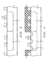
- Semiconductor substrate 1 comprised of a P type, single crystalline silicon substrate, with a ⁇ 100> crystallographic orientation, is used and schematically shown in Fig. 1 .
- P well region 2 to be used to accommodate the NMOS device, is formed in a first region of semiconductor substrate 1.
- a photoresist shape (not shown in the drawings), is used as a block out mask, allowing implantation of boron or BF 2 ions to be performed in the first region of the semiconductor substrate, resulting in the formation of P well region 2.
- another photoresist block shape is used to mask P well region 2, from an implantation procedure used to form N well region 3, in a second region of semiconductor substrate 1. This is accomplished via implantation of arsenic or phosphorous ions.
- the photoresist block out shape is again removed via plasma oxygen ashing procedures.
- additional implantation procedures are performed to form punch through and threshold voltage adjust regions in top portions of both well regions. These regions are not shown in the drawings.
- a photoresist shape (not shown in the drawings), is next use as an etch mask to allow definition of the dummy mask gate shapes comprised of silicon nitride layer 5, on pad silicon oxide layer 4.
- the definition of the dummy gate mask shapes is accomplished via an anisotropic reactive ion etch (RIE), procedure, using CF 4 or Cl 2 as an etchant for silicon nitride, while using CHF 3 as a selective etchant for silicon oxide layer 4, with the RIE procedure selectively terminating with the appearance of the top surface of semiconductor substrate 1.
- RIE anisotropic reactive ion etch
- the photoresist shape used for definition of the dummy gate mask shapes is removed via plasma oxygen ashing.
- Photoresist shape 6 is next formed and used to protect N well region 3, located in the PMOS region of semiconductor substrate 1, from an implantation procedure used to define heavily doped N type source/drain regions 7, in P well region 2. This is accomplished using arsenic or phosphorous ions, implanted at an energy between about 1 to 100 KeV, at a dose between about 1E15 to 5E15 atoms/cm 2 . The result of this procedure is schematically shown in Fig. 4 . After removal of photoresist shape 6, via plasma oxygen ashing procedures, photoresist shape 8, is formed and used to block out the NMOS region of semiconductor substrate 1, from an implantation procedure used to form heavily doped P type source/drain regions 9, in N well region 3, located in the PMOS region of semiconductor substrate 1.
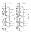
- a silicon oxide layer is next deposited to a thickness between about 50 to 1000 Angstroms, via LPCVD or PECVD procedures using tetraethylorthosilicate (TEOS), as a source. Narrow spaces between the dummy gate mask shapes located on both well regions are completely filled by the silicon oxide layer, while the wider spacers located between a dummy gate mask shape on a well region and a dummy gate mask shape located outside a well region, are not filled by the silicon oxide layer.
- TEOS tetraethylorthosilicate
- the result of these procedures is schematically shown in Fig. 6 .
- shallow trench shapes 11 is next addressed and schematically shown using Fig. 7 .
- a selective RIE procedure is employed to remove regions of semiconductor substrate 1, exposed in the wide spaces between dummy gate mask shapes, which are lined with silicon oxide spacers 10a.
- the selective RIE procedure is accomplished using SF 6 as the etchant for silicon, with a high etch rate ratio of silicon to either silicon nitride or silicon oxide, allowing shallow trench shapes 11, to be defined using silicon nitride of dummy gate mask shapes, and silicon oxide spacers 10a, as an etch mask.
- Silicon oxide shapes 10b located in the narrow spaces between dummy gate mask shapes, protected underlying well regions from this dry etch procedure.
- Shallow trench shapes 11, formed to a depth between about 1500 to 7000 Angstroms in semiconductor substrate 1, are located at the interface between P well region 2, and N well region 3, as well as at the interface between the well regions and the non-well regions of semiconductor substrate 1.
- Shallow trench shapes 11, are defined with a taper between about 75 to 90°, to optimize the filling of these shapes via subsequent CVD procedures.
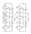
- a thin liner silicon dioxide layer is thermally grown on the exposed surfaces of the shallow trench shapes.
- the liner layer not shown in the drawings, formed at a thickness between about 30 to 500 Angstroms, offers improved dielectric integrity when compared to a subsequent CVD silicon oxide layer used to completely fill the shallow trench shapes.
- Silicon oxide layer 12 is now deposited at a thickness between about 30 to 1000 Angstroms, via LPCVD or PECVD procedures using TEOS as a source, completely filling shallow trench shapes 11. Portions of silicon oxide layer 12, are also deposited overlying the top surface of silicon nitride layer 5, of dummy gate mask shapes, as well as overlying silicon oxide shapes 10b.
- CMP chemical mechanical polishing
- An anneal procedure is next performed at a temperature between about 500 to 1200° C, in an inert ambient, for purposes of densifying the chemically vapor deposited silicon oxide layer 12.
- the densification procedure results in the evolution STI regions 13a, now comprised of silicon oxide layer 12, in shallow trench shapes 11, and comprised of silicon oxide spacers 10a, previously located on the sides of dummy gate mask shapes.
- STI regions 13b are defined in the narrow spaces located between dummy gate mask shapes, with STI regions 13b, comprised with a bottom portion featuring silicon oxide shape 10b, and comprised with a top portion featuring silicon oxide layer 12.
- the result of the anneal procedure is schematically shown in Fig. 9 .
- Silicon nitride layer 5 is selectively removed via use of a hot phosphoric acid solution, exposing the top surface of pad silicon dioxide layer 4, located between the STI regions. If desired silicon nitride layer 5, can be removed via a RIE procedure using Cl 2 as a selective etchant for silicon nitride. Pad silicon dioxide layer 4, is next selectively removed via a RIE procedure using CHF 3 as an etchant. This procedure also results in some removal of silicon oxide from the top of the STI regions. All portions of the heavily doped source/drain regions, in both well regions, are entirely located underlying STI regions 13a, and STI regions 13b.
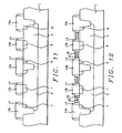
- a silicon nitride layer is next deposited at a thickness between about 30 to 1000 Angstroms, via LPCVD or PECVD procedures. The thickness of the silicon nitride layer will subsequently determine the width of lightly doped source/drain (LDD), regions.
- LDD lightly doped source/drain
- a high dielectric constant (high k), metal oxide layer such as aluminum oxide (Al 2 O 3 ), zirconium oxide (ZrO 2 ), or hafnium oxide (HfO 2 ), is next deposited at a thickness between about 15 to 300 Angstroms, via metal organic chemical vapor deposition (MOCVD), or via atomic layer chemical vapor deposition (ALCVD) procedures.
- High k layer 15 will be used as the gate insulator layer for the CMOS device.
- the high dielectric constant of high k metal oxide layer 15, between about 7 to 500, allows the use of a thicker layer.
- the higher dielectric constant layer allows an equivalent oxide thickness (EOT), equal to the thinner, lower k dielectric counterparts, to be realized.
- conductive layer comprised of a metal such as tungsten, aluminum, aluminum - copper, copper, or tungsten silicide, at a thickness between about 50 to 1000 Angstroms, via plasma vapor deposition (PVD), or via CVD procedures.
- the conductive layer can be comprised of an in situ doped polysilicon layer.
- the thickness of the conductive layer in the spaces between STI regions is greater than the thickness of the conductive layer on the top surface of the STI regions, thus a blanket etch back or chemical mechanical polishing (CMP), procedure can be used to form the desired conductive gate structure, self- aligned to STI regions without the use of photolithographic procedures.
- CMP chemical mechanical polishing
- etch back procedures used to remove thinner portions of conductive layer and of thinner high k layer from the top surface of all STI regions is accomplished using anisotropic RIE procedures, using Cl 2 as an etchant. This is schematically shown in Fig. 12 .
- a CMP procedure can also be used to remove the thinner portions of the conductive layer from the top surface of the STI regions, again resulting in definition of conductive gate structures, self-aligned to STI structures, with the definition of the conductive gate structures again accomplished without the use of photolithographic procedures.
- Silicon nitride spacers 14 are now selectively removed from the sides of STI regions 13a, and from the sides of STI regions 13b, via use of a hot phosphoric acid solution. If desired removal of silicon nitride spacers 14, can also be accomplished via a RIE procedure using Cl 2 or CF 4 as a selective etchant for silicon nitride. Spaces 17, created by the removal of silicon nitride spacers 14, exposing portions of P well region 2, and of N well region 3, will be subjected to ion implantation procedures used to form N type LDD regions 18, in exposed portions of P well region 2, and to form P type LDD regions 19, in N well region 3.
- N type LDD regions 18, are obtained via implantation of arsenic or phosphorous ions at an energy between about 1 to 100 KeV, at a dose between about 2E13 to 5E14 atoms/cm 2
- P type LDD regions 19 are obtained via implantation of boron or BF 2 ions, at an energy between about 0.1 to 30 KeV, at a dose between about 2E13 to 5E14 atoms/cm 2
- the LDD regions are formed self-aligned to conductive gate structures 16, butting heavily doped source/drain counterparts, located underlying the STI regions. The result of these procedures are schematically shown in Fig. 13 .
- Silicon oxide layer 20 is first deposited to a thickness between about 30 to 1000 Angstroms, via LPCVD or PECVD procedures. Silicon oxide layer 20, lines the sides of conductive gate structures 16, as well as the sides of STI regions 13a and 13b, however without completely filling spaces 17. Next silicon nitride layer 21, is deposited at a thickness between about 50 to 1000 Angstroms, via LPCVD or PECVD procedures, with the composite of silicon nitride layer 21, and silicon oxide layer 20, now completely filling spaces 19.
- a photoresist shape is then used as an etch mask to allow the portions of silicon nitride layer 21, to be removed from the top surfaces of STI regions 13a, and 13b, leaving the composite insulator layer, comprised of silicon nitride layer 21, and silicon oxide layer 20, only overlying conductive gate structures 16, as well as only filling spaces 19.
- the etch procedure used to accomplish this is a RIE procedure, employing CF 4 or Cl 2 as a selective etchant for silicon nitride.
- the photoresist shape used protect specific regions during the silicon nitride removal procedure, is then removed via plasma oxygen ashing procedures. If desired a CMP procedure can be used to remove the portions of silicon nitride layer 21, from the top surface of the STI regions, while other portions of silicon nitride layer 21, located on the shorter conductive gate structures, are left remaining.
- a CMP procedure is used for planarization purposes, resulting in a smooth top surface topography for ILD layer 22.
- a photoresist shape is used as an etch mask to allow openings 23, to be defined in ILD layer 22, as well as in portions of STI regions 13a, and 13b, exposing portions of the top surfaces of the heavily doped source/drain regions in both P well region 2, and N well region 3.
- Openings 23, are formed via a RIE procedure using CHF 3 as a selective etchant for silicon oxide or BPSG, therefore openings 23, butt silicon nitride component 21, of the composite insulator fill located in spaces 17.
- the presence of silicon nitride component 21, offers protection to the conductive gate structure and to the underlying high k gate insulator layer, during definition of openings 23, as well as during subsequent metal silicide formation procedures.
- the result of the above procedures is schematically shown in Fig. 15 .
- a metal layer such as cobalt, nickel, titanium, or tantalum, is deposited via PVD procedures, to a thickness between about 30 to 1000 Angstroms.
- An anneal procedure is performed using either conventional furnace procedures, or via use of rapid thermal anneal (RTA), procedures, resulting in formation of metal silicide on portions of the heavily doped source/drain regions exposed in openings 23.
- RTA rapid thermal anneal
- the metal silicide layers are not shown in the drawings. Portions of the metal layer located on the top surface of ILD layer 22, or on the inside walls of openings 22, remain unreacted and are selectively removed via wet etch procedures.
- a metal layer such as tungsten is next deposited via PVD or CVD procedures, at a thickness between about 500 to 5000 Angstroms, completely filling openings 22. Portions of the metal layer are then removed from the top surface of ILD layer 22, via a CMP procedure, resulting in formation of metal contact and interconnect structures 24, in openings 23, overlying and contacting N type heavily doped source/drain regions 7, located in P well region 2, of the NMOS device, and overlying and contacting P type heavily doped source/drain regions 9, located in N well region 3, of the PMOS device.
Abstract
Description
- The present invention relates to methods used to fabricate semiconductor devices, and more specifically to a method used to self - align a damascene type gate structure to isolation regions.
- Micro-miniaturization, or the ability to fabricate semiconductor devices comprised with sub-micron features, has been directly related to advances in photolithography. The use of more sophisticated exposure cameras as well as the use of more advanced photosensitive materials have allowed the desired sub-micron images to be defined in photoresist layers. The same photoresist layers comprised with the sub-micron images, are than used as an etch mask to allow the sub-micron images or features to be transferred to materials used for semiconductor device via anisotropic dry etching procedures. However the ability to correctly align or overlay overlying sub-micron features to underlying sub-micron features can still present problems.
- The present invention will describe a novel process sequence in which a gate structure, and an underlying gate insulator layer, are formed, self-aligned to existing isolation regions. This novel process sequence employs only a single photolithographic procedure, and a single photolithographic mask or reticle, to form the isolation regions, the subsequent self-aligned gate insulator layer and the gate structure. The gate structure and underlying gate insulator layer, can be formed via damascene procedures, with the gate insulator layer comprised of a high dielectric constant (high k) gate insulator layer. Prior arts such as: Ang et al, in
- In
U.S. Pat. No. 6 204 137 Teo et. al; inU.S. Pat. No. 6,258,677 1 U.S. Pat. No. 6,261,887 B1 ; Hsieh et al, inU.S. Pat. No. 6,248,634 ; and Tsutsumi, inU.S. Pat. No. 5,789,792 , describe methods of integrating gate structures with already formed isolation regions. However none of these prior arts describe the novel process sequence described in this present invention in which a damascene type gate structure and gate insulator layer are defined self-aligned to isolation regions. - It is an object of this invention to fabricate a semiconductor device in which the gate structure, and underlying gate insulator layer are self-aligned to isolation regions.
- It is another object of this invention to define a damascene type, gate structure and gate insulator layer, self-aligned to isolation regions without the use of a photolithographic procedure for definition of the gate structures.
- In accordance with the present invention a method of forming a gate structure and underlying gate insulator shape, self-aligned to isolation regions, is described. Silicon nitride shapes are formed on the top surface of both P well and N well regions located in top portions of a semiconductor substrate. After formation of the heavily doped source/drain regions, in portions of the P well and N well regions not covered by the silicon nitride shapes, silicon oxide spacers are formed on the sides of the silicon nitride shapes, overlying portions of the heavily doped source/drain regions. Photolithographic and dry etching procedures are then employed to form shallow trench shapes in portions of the semiconductor substrate located between the silicon nitride shapes, which are lined with the silicon oxide spacers. Filling of the shallow trench shapes with silicon oxide is followed by densification and planarization procedures resulting in shallow trench isolation (STI) structures, with bottom portions of the STI structures located in the P well and N well regions of the semiconductor substrate, while overlying top portions of the STI structures are located between the silicon nitride shapes. Selective removal of the silicon nitride shapes results in STI structures now comprised with, and widened by the addition of the remaining silicon oxide spacers. After formation of silicon nitride spacers on the sides of the STI structures, a high dielectric constant (high k) layer, and a conductive layer are deposited, followed by an etch back procedure resulting in a damascene type conductive gate structure and a high k gate insulator layer located between the silicon nitride spacers, which in turn are located on the sides of the exposed STI structures. Selective removal of the silicon nitride spacers allows the formation of lightly doped source/drain (LDD) regions, to be accomplished in the vacated space, with the LDD regions butting the heavily doped source/drain regions located under the STI regions. Refilling of the spaces created by removal of the silicon nitride spacers, with a silicon nitride - silicon oxide composite layer is followed by deposition of an interlevel dielectric (ILD) layer. Openings to the heavily doped source/drain regions in both P well and N well regions, are then accomplished in the ILD layer and in top portions of the STI structures, via selective dry etching procedures, using the silicon nitride component of the composite layer as a sidewall etch stop layer. Deposition of a metal layer, filling the openings, is followed by patterning procedures defining the desired metal contact and interconnect structures.
- The object and other advantages of this invention are best described in the preferred embodiments with reference to the attached drawings that include:
-
Figs. 1-15 , which schematically, in cross-sectional style, describe key stages used to fabricate a gate structure and underlying gate insulator shape, both self-aligned to isolation regions. - The method of forming a complimentary metal oxide semiconductor (CMOS) device, comprised with an N channel, metal oxide semiconductor (NMOS) device, and a P channel, metal oxide semiconductor (PMOS), and featuring a fabrication procedure allowing self-alignment of a gate structure and an underlying gate insulator layer to isolation regions, will now be described in detail. Semiconductor substrate 1, comprised of a P type, single crystalline silicon substrate, with a <100> crystallographic orientation, is used and schematically shown in
Fig. 1 .P well region 2, to be used to accommodate the NMOS device, is formed in a first region of semiconductor substrate 1. A photoresist shape (not shown in the drawings), is used as a block out mask, allowing implantation of boron or BF2 ions to be performed in the first region of the semiconductor substrate, resulting in the formation ofP well region 2. After removal of the photoresist block out shape (not shown in the drawings), via plasma oxygen ashing procedures, another photoresist block shape is used to maskP well region 2, from an implantation procedure used to form Nwell region 3, in a second region of semiconductor substrate 1. This is accomplished via implantation of arsenic or phosphorous ions. The photoresist block out shape is again removed via plasma oxygen ashing procedures. During the well formation procedures additional implantation procedures are performed to form punch through and threshold voltage adjust regions in top portions of both well regions. These regions are not shown in the drawings. - The attainment of dummy gate mask shapes, to be used for definition of the heavily doped source/drain regions for the NMOS device in
P well region 2, and for the PMOS device inN well region 3, is next addressed and described usingFigs. 2 - 3 .Silicon dioxide layer 4, to be used as a pad oxide layer, is first formed on the top surface of semiconductor substrate 1, at a thickness between about 30 to 1000 Angstroms (1 Angstrom = 0.1 nm), via thermal oxidation procedures, or via low pressure chemical vapor deposition (LPCVD), or plasma enhanced chemical vapor deposition (PECVD), procedures. Overlyingsilicon nitride layer 5, is then deposited at a thickness between about 50 to 2000 Angstroms, via LPCVD or PECVD procedures. A photoresist shape, (not shown in the drawings), is next use as an etch mask to allow definition of the dummy mask gate shapes comprised ofsilicon nitride layer 5, on padsilicon oxide layer 4. The definition of the dummy gate mask shapes is accomplished via an anisotropic reactive ion etch (RIE), procedure, using CF4 or Cl2 as an etchant for silicon nitride, while using CHF3 as a selective etchant forsilicon oxide layer 4, with the RIE procedure selectively terminating with the appearance of the top surface of semiconductor substrate 1. The photoresist shape used for definition of the dummy gate mask shapes is removed via plasma oxygen ashing. -
Photoresist shape 6, is next formed and used to protect Nwell region 3, located in the PMOS region of semiconductor substrate 1, from an implantation procedure used to define heavily doped N type source/drain regions 7, inP well region 2. This is accomplished using arsenic or phosphorous ions, implanted at an energy between about 1 to 100 KeV, at a dose between about 1E15 to 5E15 atoms/cm2. The result of this procedure is schematically shown inFig. 4 . After removal ofphotoresist shape 6, via plasma oxygen ashing procedures,photoresist shape 8, is formed and used to block out the NMOS region of semiconductor substrate 1, from an implantation procedure used to form heavily doped P type source/drain regions 9, in Nwell region 3, located in the PMOS region of semiconductor substrate 1. This is accomplished using boron of BF2, implanted at an energy between about 0.1 to 30 KeV, at a dose between about 1E15 to 5E15 atoms/cm2. The result of this procedure is schematically illustrated usingFig. 5 . At the completion of the implantation procedure used to define heavily doped P type source/drain regions 9,photoresist shape 8, is removed using plasma oxygen ashing procedures. - A silicon oxide layer is next deposited to a thickness between about 50 to 1000 Angstroms, via LPCVD or PECVD procedures using tetraethylorthosilicate (TEOS), as a source. Narrow spaces between the dummy gate mask shapes located on both well regions are completely filled by the silicon oxide layer, while the wider spacers located between a dummy gate mask shape on a well region and a dummy gate mask shape located outside a well region, are not filled by the silicon oxide layer. A blanket, anisotropic RIE procedure, using CHF3 as an etchant for silicon oxide, is next employed to form
silicon oxide spacers 10a, on the sides of dummy gate mask shapes exposed in the wider spaces, while the narrower spaces between dummy gate mask shapes are filled withsilicon oxide shapes 10b. The result of these procedures is schematically shown inFig. 6 . - The definition of
shallow trench shapes 11, is next addressed and schematically shown usingFig. 7 . A selective RIE procedure is employed to remove regions of semiconductor substrate 1, exposed in the wide spaces between dummy gate mask shapes, which are lined withsilicon oxide spacers 10a. The selective RIE procedure is accomplished using SF6 as the etchant for silicon, with a high etch rate ratio of silicon to either silicon nitride or silicon oxide, allowing shallow trench shapes 11, to be defined using silicon nitride of dummy gate mask shapes, andsilicon oxide spacers 10a, as an etch mask. Silicon oxide shapes 10b, located in the narrow spaces between dummy gate mask shapes, protected underlying well regions from this dry etch procedure. Shallow trench shapes 11, formed to a depth between about 1500 to 7000 Angstroms in semiconductor substrate 1, are located at the interface betweenP well region 2, and N wellregion 3, as well as at the interface between the well regions and the non-well regions of semiconductor substrate 1. Shallow trench shapes 11, are defined with a taper between about 75 to 90°, to optimize the filling of these shapes via subsequent CVD procedures. - Prior to the insulator filling of shallow trench shapes 11, a thin liner silicon dioxide layer is thermally grown on the exposed surfaces of the shallow trench shapes. The liner layer, not shown in the drawings, formed at a thickness between about 30 to 500 Angstroms, offers improved dielectric integrity when compared to a subsequent CVD silicon oxide layer used to completely fill the shallow trench shapes.
Silicon oxide layer 12, is now deposited at a thickness between about 30 to 1000 Angstroms, via LPCVD or PECVD procedures using TEOS as a source, completely filling shallow trench shapes 11. Portions ofsilicon oxide layer 12, are also deposited overlying the top surface ofsilicon nitride layer 5, of dummy gate mask shapes, as well as overlying silicon oxide shapes 10b. A chemical mechanical polishing (CMP), procedures is next employed for planarization procedures, selectively removing portions ofsilicon oxide layer 12, from the top surface ofsilicon nitride layer 5, resulting in insulator, or silicon oxide filled shallow trench shapes. This is schematically shown inFig. 8 . - An anneal procedure is next performed at a temperature between about 500 to 1200° C, in an inert ambient, for purposes of densifying the chemically vapor deposited
silicon oxide layer 12. The densification procedure results in the evolution STI regions 13a, now comprised ofsilicon oxide layer 12, in shallow trench shapes 11, and comprised ofsilicon oxide spacers 10a, previously located on the sides of dummy gate mask shapes. Inaddition STI regions 13b, are defined in the narrow spaces located between dummy gate mask shapes, withSTI regions 13b, comprised with a bottom portion featuringsilicon oxide shape 10b, and comprised with a top portion featuringsilicon oxide layer 12. The result of the anneal procedure is schematically shown inFig. 9 . - Removal of the dummy gate mask shapes is next addressed and schematically illustrated using
Fig. 10 .Silicon nitride layer 5, is selectively removed via use of a hot phosphoric acid solution, exposing the top surface of padsilicon dioxide layer 4, located between the STI regions. If desiredsilicon nitride layer 5, can be removed via a RIE procedure using Cl2 as a selective etchant for silicon nitride. Padsilicon dioxide layer 4, is next selectively removed via a RIE procedure using CHF3 as an etchant. This procedure also results in some removal of silicon oxide from the top of the STI regions. All portions of the heavily doped source/drain regions, in both well regions, are entirely located underlying STI regions 13a, andSTI regions 13b. A silicon nitride layer is next deposited at a thickness between about 30 to 1000 Angstroms, via LPCVD or PECVD procedures. The thickness of the silicon nitride layer will subsequently determine the width of lightly doped source/drain (LDD), regions. An anisotopic RIE procedure, using CF4 or Cl2 as a selective etchant for silicon nitride, is then used to definesilicon nitride spacers 14, on the sides of STI regions 13a, and on the sides ofSTI regions 13b. The result of these procedures is schematically shown inFig. 11 . - A high dielectric constant (high k), metal oxide layer, such as aluminum oxide (Al2O3), zirconium oxide (ZrO2), or hafnium oxide (HfO2), is next deposited at a thickness between about 15 to 300 Angstroms, via metal organic chemical vapor deposition (MOCVD), or via atomic layer chemical vapor deposition (ALCVD) procedures.
High k layer 15, will be used as the gate insulator layer for the CMOS device. The high dielectric constant of high kmetal oxide layer 15, between about 7 to 500, allows the use of a thicker layer. The higher dielectric constant layer allows an equivalent oxide thickness (EOT), equal to the thinner, lower k dielectric counterparts, to be realized. This is followed by deposition of conductive layer comprised of a metal such as tungsten, aluminum, aluminum - copper, copper, or tungsten silicide, at a thickness between about 50 to 1000 Angstroms, via plasma vapor deposition (PVD), or via CVD procedures. If desired the conductive layer can be comprised of an in situ doped polysilicon layer. The thickness of the conductive layer in the spaces between STI regions is greater than the thickness of the conductive layer on the top surface of the STI regions, thus a blanket etch back or chemical mechanical polishing (CMP), procedure can be used to form the desired conductive gate structure, self- aligned to STI regions without the use of photolithographic procedures. The etch back procedures used to remove thinner portions of conductive layer and of thinner high k layer from the top surface of all STI regions is accomplished using anisotropic RIE procedures, using Cl2 as an etchant. This is schematically shown inFig. 12 . If desired a CMP procedure can also be used to remove the thinner portions of the conductive layer from the top surface of the STI regions, again resulting in definition of conductive gate structures, self-aligned to STI structures, with the definition of the conductive gate structures again accomplished without the use of photolithographic procedures. -
Silicon nitride spacers 14, are now selectively removed from the sides of STI regions 13a, and from the sides ofSTI regions 13b, via use of a hot phosphoric acid solution. If desired removal ofsilicon nitride spacers 14, can also be accomplished via a RIE procedure using Cl2 or CF4 as a selective etchant for silicon nitride.Spaces 17, created by the removal ofsilicon nitride spacers 14, exposing portions ofP well region 2, and ofN well region 3, will be subjected to ion implantation procedures used to form Ntype LDD regions 18, in exposed portions ofP well region 2, and to form Ptype LDD regions 19, inN well region 3. Photoresist block out shapes are used to protect each specific well region during implantation procedures performed to the other specific well region. Ntype LDD regions 18, are obtained via implantation of arsenic or phosphorous ions at an energy between about 1 to 100 KeV, at a dose between about 2E13 to 5E14 atoms/cm2, while Ptype LDD regions 19, are obtained via implantation of boron or BF2 ions, at an energy between about 0.1 to 30 KeV, at a dose between about 2E13 to 5E14 atoms/cm2. The LDD regions are formed self-aligned toconductive gate structures 16, butting heavily doped source/drain counterparts, located underlying the STI regions. The result of these procedures are schematically shown inFig. 13 . - Refilling of
spaces 17, created by the removal ofsilicon nitride spacers 14, is next addressed and schematically shown inFig. 14 .Silicon oxide layer 20, is first deposited to a thickness between about 30 to 1000 Angstroms, via LPCVD or PECVD procedures.Silicon oxide layer 20, lines the sides ofconductive gate structures 16, as well as the sides ofSTI regions 13a and 13b, however without completely fillingspaces 17. Nextsilicon nitride layer 21, is deposited at a thickness between about 50 to 1000 Angstroms, via LPCVD or PECVD procedures, with the composite ofsilicon nitride layer 21, andsilicon oxide layer 20, now completely fillingspaces 19. A photoresist shape, not shown in the drawings, is then used as an etch mask to allow the portions ofsilicon nitride layer 21, to be removed from the top surfaces ofSTI regions 13a, and 13b, leaving the composite insulator layer, comprised ofsilicon nitride layer 21, andsilicon oxide layer 20, only overlyingconductive gate structures 16, as well as only fillingspaces 19. The etch procedure used to accomplish this is a RIE procedure, employing CF4 or Cl2 as a selective etchant for silicon nitride. The photoresist shape used protect specific regions during the silicon nitride removal procedure, is then removed via plasma oxygen ashing procedures. If desired a CMP procedure can be used to remove the portions ofsilicon nitride layer 21, from the top surface of the STI regions, while other portions ofsilicon nitride layer 21, located on the shorter conductive gate structures, are left remaining. - Interlevel dielectric (ILD),
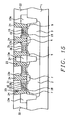
layer 22, comprised of silicon oxide or borophosphosilicate glass (BPSG), is next deposited to a thickness between about 500 to 1000 Angstroms via LPCVD or PECVD procedures. A CMP procedure is used for planarization purposes, resulting in a smooth top surface topography forILD layer 22. A photoresist shape, not shown in the drawings, is used as an etch mask to allowopenings 23, to be defined inILD layer 22, as well as in portions ofSTI regions 13a, and 13b, exposing portions of the top surfaces of the heavily doped source/drain regions in bothP well region 2, and N wellregion 3.Openings 23, are formed via a RIE procedure using CHF3 as a selective etchant for silicon oxide or BPSG, thereforeopenings 23, buttsilicon nitride component 21, of the composite insulator fill located inspaces 17. The presence ofsilicon nitride component 21, offers protection to the conductive gate structure and to the underlying high k gate insulator layer, during definition ofopenings 23, as well as during subsequent metal silicide formation procedures. The result of the above procedures is schematically shown inFig. 15 . - After removal of the photoresist shape used for definition of
openings 23, via plasma oxygen ashing procedures, a metal layer such as cobalt, nickel, titanium, or tantalum, is deposited via PVD procedures, to a thickness between about 30 to 1000 Angstroms. An anneal procedure is performed using either conventional furnace procedures, or via use of rapid thermal anneal (RTA), procedures, resulting in formation of metal silicide on portions of the heavily doped source/drain regions exposed inopenings 23. The metal silicide layers are not shown in the drawings. Portions of the metal layer located on the top surface ofILD layer 22, or on the inside walls ofopenings 22, remain unreacted and are selectively removed via wet etch procedures. A metal layer such as tungsten, is next deposited via PVD or CVD procedures, at a thickness between about 500 to 5000 Angstroms, completely fillingopenings 22. Portions of the metal layer are then removed from the top surface ofILD layer 22, via a CMP procedure, resulting in formation of metal contact andinterconnect structures 24, inopenings 23, overlying and contacting N type heavily doped source/drain regions 7, located inP well region 2, of the NMOS device, and overlying and contacting P type heavily doped source/drain regions 9, located inN well region 3, of the PMOS device.
Claims (23)
- A method of fabricating a metal oxide semiconductor field effect transistor (MOSFET) device on a semiconductor substrate, comprising the steps of:- forming composite insulator structures (4,5) on top surfaces of first portions of said semiconductor substrate (1);- forming heavily doped source/drain regions (7) in second portions of said semiconductor substrate, not covered by said composite insulator structures;- forming first insulator spacers (10a) on sides of said composite insulator structures, with each first insulator spacer overlying and covering a portion of a heavily doped source/drain region;- defining shallow trench openings (11) in portions of said semiconductor substrate not covered by said composite insulator structures or by said first insulator spacers;- filling said shallow trench openings, and spaces between said composite insulator structures with a first insulator layer (12), resulting in shallow trench isolation (STI) regions with each STI region comprised of an underlying insulator filled shallow trench opening, and comprised of an overlying first insulator shape (13a) located between composite insulator structures, with said first insulator spacers located on sides of said composite insulator structures, now a component of said overlying first insulator shape;- selectively removing said composite insulator structures;- forming second insulator spacers (14) on sides of said STI regions;- forming a gate insulator layer (15) on a portion of said semiconductor substrate not covered by said STI regions or by said second insulator spacers:- forming a conductive gate structure (16) on said gate insulator layer with said conductive gate structure self-aligned to said STI regions;- removing said second insulator spacers;- forming lightly doped source/drain regions (18, 19) in portions of said semiconductor substrate exposed by removal of said second insulator spacers, with each lightly doped source/drain region located adjacent to, and butting to a heavily doped source/drain region, which in turn is located underlying an STI region;- forming a composite insulator layer (20, 21) in space between said STI region and said conductive gate structure, with said composite insulator layer overlying said lightly doped source drain region;- depositing a second insulator layer (22);- forming openings (23) in said second insulator layer and in said STI regions to expose portions of said heavily doped source/drain regions;- forming metal silicide layers on exposed portions of said heavily doped source/drain region; and- forming metal structures (24) in said openings, with said metal structures located overlying said metal silicide layers.
- The method of claim 1, wherein said composite insulator structures are comprised of an overlying silicon nitride shape at a thickness between about 50 to 2000 Angstroms (5 to 200 nm), and comprised of an underlying silicon dioxide shape at a thickness between about 30 to 1000 Angstroms (3 to 100 nm).
- The method of claim 1, wherein said heavily doped source/drain regions are N type heavily doped source/drain regions, obtained via implantation of arsenic or phosphorous ions implanted at an energy between about 1 to 100 KeV, at a dose between about 1 E15 to 5E15 atoms/cm2.
- The method of claim 1, wherein said heavily doped source/drain regions are P type heavily doped source/drain regions, obtained via implantation of boron or BF2 ions implanted at an energy between about 0.1 to 30 KeV, at a dose between about 1E15 to 5E15 atoms/cm2.
- The method of claim 1, wherein said first insulator spacers are silicon oxide spacers, obtained from deposition of a silicon oxide layer obtained via LPCVD or PECVD procedures at a thickness between about 50 to 1000 Angstroms (5 to 100 nm), then defined via anisotropic RIE procedures using CHF3 as an etchant.
- The method of claim 1, wherein said first Insulator layer, used to fill said shallow trench openings, is a silicon oxide layer, obtained via LPCVD or PECVD procedures, at a thickness between about 30 to 500 Angstroms (3 to 50 nm), using tetraethylorthosilicate (TEOS) as a source.
- The method of claim 1, wherein said second insulator spacers are silicon nitride spacers, obtained from deposition of a silicon nitride layer at a thickness between about 30 to 1000 Angstroms (3 to 100 nm), via LPCVD or PECVD procedures, then defined via anisotropic RIE procedures using CF4 or Cl2 as an etchant.
- The method of claim 1, wherein said gate insulator layer is a high k dielectric layer, comprised of either aluminum oxide (Al2O3), zirconium oxide (ZrO2), or hafnium oxide (HfO2), obtained at a thickness between about 15 to 300 Angstroms (1.5 to 30 nm), via metal organic chemical vapor deposition (MOCVD), or via atomic layer chemical vapor deposition (LCVD) procedures.
- The method of claim 1, wherein said gate insulator layer is comprised with a dielectric constant between about 7 to 100.
- The method of claim 1, wherein said second insulator spacers are selectively removed via wet etch procedures, using hot phosphoric acid as an etchant for silicon nitride.
- The method of claim 1, wherein said lightly doped source/drain regions are N type heavily doped source/drain regions, obtained via implantation of arsenic or phosphorous ions implanted at an energy between about 1 to 100 KeV, at a dose between about 2E13 to 5E14 atoms/cm2.
- The method of claim 1, wherein said lightly doped source/drain regions are P type heavily doped source/drain regions, obtained via implantation of boron or BF2 ions Implanted at a dose between about 2E13 to 5E14 atoms/cm2.
- The method of claim 1, wherein said composite insulator layer, located in said space between said STI region and said conductive gate structure, is comprised of an underlying silicon oxide layer obtained at a thickness between about 30 to 1000 Angstroms (3 to 100 nm) via LPCVD or PECVD procedures, and comprised of an overlying silicon nitride layer obtained at a thickness between about 50 to 1000 Angstroms (5 to 100 nm) LPCVD or PECVD procedures.
- The method of claim 1 further comprising:- forming a P well region in a third portion of said semiconductor substrate to be used to accommodate an N channel metal oxide semiconductor (NMOS), device of said CMOS device; and- forming an N well region in a fourth portion of said semiconductor substrate to be used to accommodate a P channel metal oxide semiconductor (PMOS), device of said CMOS device; wherein- said composite insulator structures are formed on said top surface of said semiconductor substrate overlying said first portions of both said P well region and said N well region wherein, each of said composite insulator structures are comprised with an overlying silicon nitride shape and with an underlying silicon dioxide shape;- wherein said N type heavily doped source/drain regions are formed in said second portions of said P well region and said N well region not covered by said composite insulator structures;- whereinN type heavily doped source/drain regions are formed in said second portions of said P well region and wherein P type heavily doped source/drain regions are formed in said second portions of said N well region; and;- whereing said lightly doped source/drain regions comprise N type lightly doped source/drain regions in portions of said P well region located adjacent to, and butting to said N type heavily doped source/drain region
- The method of claim 1, wherein said metal silicide layers comprise cobalt silicide.
- The method of claim 14, wherein said N type heavily doped source/drain regions are obtained via implantation of arsenic or phosphorous implanted at an energy between about 1 to 100 KeV, at a dose between about 1E15 to 5E15 atoms/cm2.
- The method of claim 14, wherein said P type heavily doped source/drain regions are obtained via implantation of boron or BF2 ions implanted at an energy between about 0.1 to 30 KeV, at a dose between about 1E15 to 5E15 atoms/cm2.
- The method of claims 1, wherein said shallow trench openings are formed to a depth between about 1500 to 7000 Angstroms (150 to 700 nm) in said semiconductor substrate, with a taper between about 75 to 90°, via a RIE procedure using SF6 as a selective etchant for silicon.
- The method of claims 1, wherein said composite insulator spacers are removed via RIE procedures, using CF4 or Cl2 as an etchant for silicon nitride, while using CHF3 as an etchant for silicon dioxide.
- The method of claims 1, wherein said silicon nitride shapes of said composite insulator spacers are selectively removed via wet etch procedures using a hot phosphoric acid solution.
- The method of claims 1, wherein said conductive gate structure is formed at a thickness between about 50 to 1000 Angstroms, (5 to 100 nm) and is comprised of a material chosen from a group that includes; aluminum, aluminum - copper, copper, tungsten, tungsten silicide, or doped polysilicon.
- The method of claim 14, wherein said N type lightly doped source/drain regions are obtained via implantation of arsenic or phosphorous ions implanted at an energy between about 1 to 100 KeV, at a dose between about 2E13 to 5E14 atoms/cm2.
- The method of claim 14, wherein said P type lightly doped source/drain regions are obtained via implantation of boron or BF2 ions implanted at a dose between about 2E13 to 5E14 atoms/cm2.
Applications Claiming Priority (2)
| Application Number | Priority Date | Filing Date | Title |
|---|---|---|---|
| US10/225,805 US6713335B2 (en) | 2002-08-22 | 2002-08-22 | Method of self-aligning a damascene gate structure to isolation regions |
| US225805 | 2002-08-22 |
Publications (3)
| Publication Number | Publication Date |
|---|---|
| EP1391925A2 EP1391925A2 (en) | 2004-02-25 |
| EP1391925A3 EP1391925A3 (en) | 2005-04-20 |
| EP1391925B1 true EP1391925B1 (en) | 2008-07-16 |
Family
ID=31187999
Family Applications (1)
| Application Number | Title | Priority Date | Filing Date |
|---|---|---|---|
| EP03368080A Expired - Lifetime EP1391925B1 (en) | 2002-08-22 | 2003-08-20 | Method of self-aligning a damascene gate structure to isolation regions |
Country Status (7)
| Country | Link |
|---|---|
| US (1) | US6713335B2 (en) |
| EP (1) | EP1391925B1 (en) |
| JP (1) | JP2004134757A (en) |
| AT (1) | ATE401665T1 (en) |
| DE (1) | DE60322154D1 (en) |
| SG (1) | SG102720A1 (en) |
| TW (1) | TWI260732B (en) |
Families Citing this family (21)
| Publication number | Priority date | Publication date | Assignee | Title |
|---|---|---|---|---|
| TW200425298A (en) * | 2003-05-01 | 2004-11-16 | Nanya Technology Corp | Fabrication method for a damascene bitline contact |
| US20050196946A1 (en) * | 2004-03-02 | 2005-09-08 | Matsushita Electric Industrial Co., Ltd. | Method for manufacturing solid-state imaging device |
| JP4577680B2 (en) * | 2004-04-13 | 2010-11-10 | エルピーダメモリ株式会社 | Manufacturing method of semiconductor device |
| JP4054321B2 (en) * | 2004-06-23 | 2008-02-27 | 松下電器産業株式会社 | Semiconductor device |
| US7118952B2 (en) * | 2004-07-14 | 2006-10-10 | Taiwan Semiconductor Manufacturing Co., Ltd. | Method of making transistor with strained source/drain |
| US7148548B2 (en) * | 2004-07-20 | 2006-12-12 | Intel Corporation | Semiconductor device with a high-k gate dielectric and a metal gate electrode |
| US7138323B2 (en) * | 2004-07-28 | 2006-11-21 | Intel Corporation | Planarizing a semiconductor structure to form replacement metal gates |
| KR100641993B1 (en) * | 2004-12-15 | 2006-11-02 | 동부일렉트로닉스 주식회사 | Method of manufacturing CMOS image sensor having high k insulator |
| BRPI0709548A2 (en) * | 2006-03-15 | 2011-07-19 | Google Inc | automatic display of reframed images |
| TWI336918B (en) * | 2007-05-08 | 2011-02-01 | Nanya Technology Corp | Method of manufacturing the shallow trench isolation structure |
| US7998832B2 (en) * | 2008-08-27 | 2011-08-16 | Advanced Micro Devices, Inc. | Semiconductor device with isolation trench liner, and related fabrication methods |
| US8735991B2 (en) | 2011-12-01 | 2014-05-27 | Taiwan Semiconductor Manufacturing Company, Ltd. | High gate density devices and methods |
| US9865690B2 (en) * | 2012-04-10 | 2018-01-09 | Qorvo Us, Inc. | Methods for fabricating a metal structure for a semiconductor device |
| US9165838B2 (en) * | 2014-02-26 | 2015-10-20 | Taiwan Semiconductor Manufacturing Company Limited | Methods of forming low resistance contacts |
| US9530853B2 (en) | 2014-03-10 | 2016-12-27 | Qorvo Us, Inc. | Semiconductor device with reduced leakage current and method for making the same |
| DE102014107994A1 (en) * | 2014-06-05 | 2015-12-17 | Infineon Technologies Austria Ag | Semiconductor device and method for manufacturing the semiconductor device |
| US9666586B2 (en) * | 2014-08-14 | 2017-05-30 | Gil Asa | CMOS compatible memory cells |
| US9378968B2 (en) * | 2014-09-02 | 2016-06-28 | United Microelectronics Corporation | Method for planarizing semiconductor device |
| FR3036846B1 (en) * | 2015-05-29 | 2018-06-15 | Stmicroelectronics (Crolles 2) Sas | METHOD FOR LOCAL ISOLATION BETWEEN TRANSISTORS MADE ON A SOI SUBSTRATE, ESPECIALLY FDSOI, AND CORRESPONDING INTEGRATED CIRCUIT |
| US10147719B2 (en) * | 2016-11-17 | 2018-12-04 | Taiwan Semiconductor Manufacturing Co., Ltd. | Semiconductor field effect transistors and manufacturing method thereof |
| US10784359B2 (en) * | 2018-05-18 | 2020-09-22 | Taiwan Semiconductor Manufacturing Company, Ltd. | Non-conformal oxide liner and manufacturing methods thereof |
Family Cites Families (8)
| Publication number | Priority date | Publication date | Assignee | Title |
|---|---|---|---|---|
| JPH1070187A (en) | 1996-08-28 | 1998-03-10 | Mitsubishi Electric Corp | Semiconductor device and its manufacture |
| JP4160167B2 (en) * | 1997-06-30 | 2008-10-01 | 株式会社東芝 | Manufacturing method of semiconductor device |
| US6261887B1 (en) | 1997-08-28 | 2001-07-17 | Texas Instruments Incorporated | Transistors with independently formed gate structures and method |
| US6248643B1 (en) | 1999-04-02 | 2001-06-19 | Vanguard International Semiconductor Corporation | Method of fabricating a self-aligned contact |
| US6258677B1 (en) | 1999-10-01 | 2001-07-10 | Chartered Seminconductor Manufacturing Ltd. | Method of fabricating wedge isolation transistors |
| JP3538108B2 (en) * | 2000-03-14 | 2004-06-14 | 松下電器産業株式会社 | Semiconductor device and manufacturing method thereof |
| JP2001267561A (en) * | 2000-03-21 | 2001-09-28 | Sony Corp | Method of manufacturing for semiconductor device and semiconductor device |
| US6204137B1 (en) * | 2000-04-24 | 2001-03-20 | Chartered Semiconductor Manufacturing, Ltd. | Method to form transistors and local interconnects using a silicon nitride dummy gate technique |
-
2002
- 2002-08-22 US US10/225,805 patent/US6713335B2/en not_active Expired - Fee Related
-
2003
- 2003-08-05 SG SG200304568A patent/SG102720A1/en unknown
- 2003-08-05 TW TW092121331A patent/TWI260732B/en active
- 2003-08-20 EP EP03368080A patent/EP1391925B1/en not_active Expired - Lifetime
- 2003-08-20 DE DE60322154T patent/DE60322154D1/en not_active Expired - Lifetime
- 2003-08-20 AT AT03368080T patent/ATE401665T1/en not_active IP Right Cessation
- 2003-08-21 JP JP2003297152A patent/JP2004134757A/en active Pending
Also Published As
| Publication number | Publication date |
|---|---|
| TW200403803A (en) | 2004-03-01 |
| DE60322154D1 (en) | 2008-08-28 |
| EP1391925A3 (en) | 2005-04-20 |
| US6713335B2 (en) | 2004-03-30 |
| TWI260732B (en) | 2006-08-21 |
| EP1391925A2 (en) | 2004-02-25 |
| SG102720A1 (en) | 2004-03-26 |
| ATE401665T1 (en) | 2008-08-15 |
| US20040038466A1 (en) | 2004-02-26 |
| JP2004134757A (en) | 2004-04-30 |
Similar Documents
| Publication | Publication Date | Title |
|---|---|---|
| EP1391925B1 (en) | Method of self-aligning a damascene gate structure to isolation regions | |
| US7393766B2 (en) | Process for integration of a high dielectric constant gate insulator layer in a CMOS device | |
| US6300201B1 (en) | Method to form a high K dielectric gate insulator layer, a metal gate structure, and self-aligned channel regions, post source/drain formation | |
| US6303418B1 (en) | Method of fabricating CMOS devices featuring dual gate structures and a high dielectric constant gate insulator layer | |
| US6908801B2 (en) | Method of manufacturing semiconductor device | |
| US5920098A (en) | Tungsten local interconnect, using a silicon nitride capped self-aligned contact process | |
| US5766992A (en) | Process for integrating a MOSFET device, using silicon nitride spacers and a self-aligned contact structure, with a capacitor structure | |
| US20080085590A1 (en) | Method of making FUSI gate and resulting structure | |
| US6800530B2 (en) | Triple layer hard mask for gate patterning to fabricate scaled CMOS transistors | |
| KR100537580B1 (en) | Process for the fabrication of mosfet devices depletion, silicided source and drain junctions | |
| US6468877B1 (en) | Method to form an air-gap under the edges of a gate electrode by using disposable spacer/liner | |
| US5731236A (en) | Process to integrate a self-aligned contact structure, with a capacitor structure | |
| US6033962A (en) | Method of fabricating sidewall spacers for a self-aligned contact hole | |
| US6498067B1 (en) | Integrated approach for controlling top dielectric loss during spacer etching | |
| US6258678B1 (en) | Use of a wet etch dip step used as part of a self-aligned contact opening procedure | |
| KR20190064391A (en) | Semiconductor device and method of manufacture | |
| US7332394B2 (en) | Method to reduce a capacitor depletion phenomena | |
| US20040038517A1 (en) | Methods of forming cobalt silicide contact structures including sidewall spacers for electrical isolation and contact structures formed thereby | |
| US6468851B1 (en) | Method of fabricating CMOS device with dual gate electrode | |
| US7622347B2 (en) | Self-aligned metal electrode to eliminate native oxide effect for metal insulator semiconductor (MIS) capacitor | |
| US6579784B1 (en) | Method for forming a metal gate integrated with a source and drain salicide process with oxynitride spacers | |
| US6235593B1 (en) | Self aligned contact using spacers on the ILD layer sidewalls | |
| KR100697292B1 (en) | Semiconductor device and method for forming thereof | |
| US6534405B1 (en) | Method of forming a MOSFET device featuring a dual salicide process | |
| US6306741B1 (en) | Method of patterning gate electrodes with high K gate dielectrics |
Legal Events
| Date | Code | Title | Description |
|---|---|---|---|
| PUAI | Public reference made under article 153(3) epc to a published international application that has entered the european phase |
Free format text: ORIGINAL CODE: 0009012 |
|
| AK | Designated contracting states |
Kind code of ref document: A2 Designated state(s): AT BE BG CH CY CZ DE DK EE ES FI FR GB GR HU IE IT LI LU MC NL PT RO SE SI SK TR |
|
| AX | Request for extension of the european patent |
Extension state: AL LT LV MK |
|
| PUAL | Search report despatched |
Free format text: ORIGINAL CODE: 0009013 |
|
| AK | Designated contracting states |
Kind code of ref document: A3 Designated state(s): AT BE BG CH CY CZ DE DK EE ES FI FR GB GR HU IE IT LI LU MC NL PT RO SE SI SK TR |
|
| AX | Request for extension of the european patent |
Extension state: AL LT LV MK |
|
| 17P | Request for examination filed |
Effective date: 20051020 |
|
| AKX | Designation fees paid |
Designated state(s): AT BE BG CH CY CZ DE DK EE ES FI FR GB GR HU IE IT LI LU MC NL PT RO SE SI SK TR |
|
| 17Q | First examination report despatched |
Effective date: 20061005 |
|
| GRAP | Despatch of communication of intention to grant a patent |
Free format text: ORIGINAL CODE: EPIDOSNIGR1 |
|
| RIN1 | Information on inventor provided before grant (corrected) |
Inventor name: LEE, TONG BOON Inventor name: CHUNG, CHING-THIAM Inventor name: YEN, DANIEL Inventor name: NIEH, CHESTER Inventor name: CHENG, WEI HUA |
|
| GRAS | Grant fee paid |
Free format text: ORIGINAL CODE: EPIDOSNIGR3 |
|
| GRAA | (expected) grant |
Free format text: ORIGINAL CODE: 0009210 |
|
| AK | Designated contracting states |
Kind code of ref document: B1 Designated state(s): AT BE BG CH CY CZ DE DK EE ES FI FR GB GR HU IE IT LI LU MC NL PT RO SE SI SK TR |
|
| REG | Reference to a national code |
Ref country code: GB Ref legal event code: FG4D |
|
| REG | Reference to a national code |
Ref country code: CH Ref legal event code: EP |
|
| REF | Corresponds to: |
Ref document number: 60322154 Country of ref document: DE Date of ref document: 20080828 Kind code of ref document: P |
|
| REG | Reference to a national code |
Ref country code: IE Ref legal event code: FG4D |
|
| NLV1 | Nl: lapsed or annulled due to failure to fulfill the requirements of art. 29p and 29m of the patents act | ||
| PG25 | Lapsed in a contracting state [announced via postgrant information from national office to epo] |
Ref country code: ES Free format text: LAPSE BECAUSE OF FAILURE TO SUBMIT A TRANSLATION OF THE DESCRIPTION OR TO PAY THE FEE WITHIN THE PRESCRIBED TIME-LIMIT Effective date: 20081027 Ref country code: PT Free format text: LAPSE BECAUSE OF FAILURE TO SUBMIT A TRANSLATION OF THE DESCRIPTION OR TO PAY THE FEE WITHIN THE PRESCRIBED TIME-LIMIT Effective date: 20081216 Ref country code: NL Free format text: LAPSE BECAUSE OF FAILURE TO SUBMIT A TRANSLATION OF THE DESCRIPTION OR TO PAY THE FEE WITHIN THE PRESCRIBED TIME-LIMIT Effective date: 20080716 |
|
| PG25 | Lapsed in a contracting state [announced via postgrant information from national office to epo] |
Ref country code: SI Free format text: LAPSE BECAUSE OF FAILURE TO SUBMIT A TRANSLATION OF THE DESCRIPTION OR TO PAY THE FEE WITHIN THE PRESCRIBED TIME-LIMIT Effective date: 20080716 Ref country code: FI Free format text: LAPSE BECAUSE OF FAILURE TO SUBMIT A TRANSLATION OF THE DESCRIPTION OR TO PAY THE FEE WITHIN THE PRESCRIBED TIME-LIMIT Effective date: 20080716 Ref country code: BG Free format text: LAPSE BECAUSE OF FAILURE TO SUBMIT A TRANSLATION OF THE DESCRIPTION OR TO PAY THE FEE WITHIN THE PRESCRIBED TIME-LIMIT Effective date: 20081016 Ref country code: AT Free format text: LAPSE BECAUSE OF FAILURE TO SUBMIT A TRANSLATION OF THE DESCRIPTION OR TO PAY THE FEE WITHIN THE PRESCRIBED TIME-LIMIT Effective date: 20080716 |
|
| PG25 | Lapsed in a contracting state [announced via postgrant information from national office to epo] |
Ref country code: MC Free format text: LAPSE BECAUSE OF NON-PAYMENT OF DUE FEES Effective date: 20080831 |
|
| REG | Reference to a national code |
Ref country code: CH Ref legal event code: PL |
|
| PG25 | Lapsed in a contracting state [announced via postgrant information from national office to epo] |
Ref country code: DK Free format text: LAPSE BECAUSE OF FAILURE TO SUBMIT A TRANSLATION OF THE DESCRIPTION OR TO PAY THE FEE WITHIN THE PRESCRIBED TIME-LIMIT Effective date: 20080716 Ref country code: EE Free format text: LAPSE BECAUSE OF FAILURE TO SUBMIT A TRANSLATION OF THE DESCRIPTION OR TO PAY THE FEE WITHIN THE PRESCRIBED TIME-LIMIT Effective date: 20080716 |
|
| PLBE | No opposition filed within time limit |
Free format text: ORIGINAL CODE: 0009261 |
|
| STAA | Information on the status of an ep patent application or granted ep patent |
Free format text: STATUS: NO OPPOSITION FILED WITHIN TIME LIMIT |
|
| REG | Reference to a national code |
Ref country code: IE Ref legal event code: MM4A |
|
| PG25 | Lapsed in a contracting state [announced via postgrant information from national office to epo] |
Ref country code: SK Free format text: LAPSE BECAUSE OF FAILURE TO SUBMIT A TRANSLATION OF THE DESCRIPTION OR TO PAY THE FEE WITHIN THE PRESCRIBED TIME-LIMIT Effective date: 20080716 Ref country code: RO Free format text: LAPSE BECAUSE OF FAILURE TO SUBMIT A TRANSLATION OF THE DESCRIPTION OR TO PAY THE FEE WITHIN THE PRESCRIBED TIME-LIMIT Effective date: 20080716 Ref country code: CZ Free format text: LAPSE BECAUSE OF FAILURE TO SUBMIT A TRANSLATION OF THE DESCRIPTION OR TO PAY THE FEE WITHIN THE PRESCRIBED TIME-LIMIT Effective date: 20080716 |
|
| 26N | No opposition filed |
Effective date: 20090417 |
|
| GBPC | Gb: european patent ceased through non-payment of renewal fee |
Effective date: 20081016 |
|
| PG25 | Lapsed in a contracting state [announced via postgrant information from national office to epo] |
Ref country code: LI Free format text: LAPSE BECAUSE OF NON-PAYMENT OF DUE FEES Effective date: 20080831 Ref country code: CH Free format text: LAPSE BECAUSE OF NON-PAYMENT OF DUE FEES Effective date: 20080831 |
|
| PG25 | Lapsed in a contracting state [announced via postgrant information from national office to epo] |
Ref country code: IE Free format text: LAPSE BECAUSE OF NON-PAYMENT OF DUE FEES Effective date: 20080820 |
|
| PG25 | Lapsed in a contracting state [announced via postgrant information from national office to epo] |
Ref country code: IT Free format text: LAPSE BECAUSE OF FAILURE TO SUBMIT A TRANSLATION OF THE DESCRIPTION OR TO PAY THE FEE WITHIN THE PRESCRIBED TIME-LIMIT Effective date: 20080716 |
|
| PG25 | Lapsed in a contracting state [announced via postgrant information from national office to epo] |
Ref country code: GB Free format text: LAPSE BECAUSE OF NON-PAYMENT OF DUE FEES Effective date: 20081016 |
|
| PG25 | Lapsed in a contracting state [announced via postgrant information from national office to epo] |
Ref country code: SE Free format text: LAPSE BECAUSE OF FAILURE TO SUBMIT A TRANSLATION OF THE DESCRIPTION OR TO PAY THE FEE WITHIN THE PRESCRIBED TIME-LIMIT Effective date: 20081016 |
|
| PG25 | Lapsed in a contracting state [announced via postgrant information from national office to epo] |
Ref country code: LU Free format text: LAPSE BECAUSE OF NON-PAYMENT OF DUE FEES Effective date: 20080820 Ref country code: CY Free format text: LAPSE BECAUSE OF FAILURE TO SUBMIT A TRANSLATION OF THE DESCRIPTION OR TO PAY THE FEE WITHIN THE PRESCRIBED TIME-LIMIT Effective date: 20080716 Ref country code: HU Free format text: LAPSE BECAUSE OF FAILURE TO SUBMIT A TRANSLATION OF THE DESCRIPTION OR TO PAY THE FEE WITHIN THE PRESCRIBED TIME-LIMIT Effective date: 20090117 |
|
| PG25 | Lapsed in a contracting state [announced via postgrant information from national office to epo] |
Ref country code: TR Free format text: LAPSE BECAUSE OF FAILURE TO SUBMIT A TRANSLATION OF THE DESCRIPTION OR TO PAY THE FEE WITHIN THE PRESCRIBED TIME-LIMIT Effective date: 20080716 |
|
| PG25 | Lapsed in a contracting state [announced via postgrant information from national office to epo] |
Ref country code: GR Free format text: LAPSE BECAUSE OF FAILURE TO SUBMIT A TRANSLATION OF THE DESCRIPTION OR TO PAY THE FEE WITHIN THE PRESCRIBED TIME-LIMIT Effective date: 20081017 |
|
| PGFP | Annual fee paid to national office [announced via postgrant information from national office to epo] |
Ref country code: DE Payment date: 20100826 Year of fee payment: 8 Ref country code: FR Payment date: 20100902 Year of fee payment: 8 |
|
| PGFP | Annual fee paid to national office [announced via postgrant information from national office to epo] |
Ref country code: BE Payment date: 20100824 Year of fee payment: 8 |
|
| REG | Reference to a national code |
Representative=s name: GRUENECKER, DE Ref country code: DE Ref legal event code: R082 Ref document number: 60322154 Country of ref document: DE |
|
| BERE | Be: lapsed |
Owner name: CHARTERED SEMICONDUCTOR MANUFACTURING PTE LTD. Effective date: 20110831 |
|
| REG | Reference to a national code |
Ref country code: DE Ref legal event code: R082 Ref document number: 60322154 Country of ref document: DE Representative=s name: GRUENECKER, KINKELDEY, STOCKMAIR & SCHWANHAEUS, DE Effective date: 20120120 Ref country code: DE Ref legal event code: R081 Ref document number: 60322154 Country of ref document: DE Owner name: GLOBALFOUNDRIES SINGAPORE PTE. LTD., SG Free format text: FORMER OWNER: CHARTERED SEMICONDUCTOR MFG. PTE. LTD., SINGAPUR/SINGAPORE, SG Effective date: 20120227 Ref country code: DE Ref legal event code: R082 Ref document number: 60322154 Country of ref document: DE Representative=s name: GRUENECKER PATENT- UND RECHTSANWAELTE PARTG MB, DE Effective date: 20120120 |
|
| REG | Reference to a national code |
Ref country code: FR Ref legal event code: ST Effective date: 20120430 |
|
| PG25 | Lapsed in a contracting state [announced via postgrant information from national office to epo] |
Ref country code: BE Free format text: LAPSE BECAUSE OF NON-PAYMENT OF DUE FEES Effective date: 20110831 |
|
| REG | Reference to a national code |
Ref country code: DE Ref legal event code: R119 Ref document number: 60322154 Country of ref document: DE Effective date: 20120301 |
|
| PG25 | Lapsed in a contracting state [announced via postgrant information from national office to epo] |
Ref country code: FR Free format text: LAPSE BECAUSE OF NON-PAYMENT OF DUE FEES Effective date: 20110831 |
|
| PG25 | Lapsed in a contracting state [announced via postgrant information from national office to epo] |
Ref country code: DE Free format text: LAPSE BECAUSE OF NON-PAYMENT OF DUE FEES Effective date: 20120301 |