EP1367820A2 - Videosignalsverarbeitungsvorrichtung - Google Patents
Videosignalsverarbeitungsvorrichtung Download PDFInfo
- Publication number
- EP1367820A2 EP1367820A2 EP03011225A EP03011225A EP1367820A2 EP 1367820 A2 EP1367820 A2 EP 1367820A2 EP 03011225 A EP03011225 A EP 03011225A EP 03011225 A EP03011225 A EP 03011225A EP 1367820 A2 EP1367820 A2 EP 1367820A2
- Authority
- EP
- European Patent Office
- Prior art keywords
- video signal
- signal
- progressive
- interlaced
- field
- Prior art date
- Legal status (The legal status is an assumption and is not a legal conclusion. Google has not performed a legal analysis and makes no representation as to the accuracy of the status listed.)
- Withdrawn
Links
Images


Classifications
-
- H—ELECTRICITY
- H04—ELECTRIC COMMUNICATION TECHNIQUE
- H04N—PICTORIAL COMMUNICATION, e.g. TELEVISION
- H04N7/00—Television systems
- H04N7/01—Conversion of standards, e.g. involving analogue television standards or digital television standards processed at pixel level
-
- H—ELECTRICITY
- H04—ELECTRIC COMMUNICATION TECHNIQUE
- H04N—PICTORIAL COMMUNICATION, e.g. TELEVISION
- H04N5/00—Details of television systems
- H04N5/44—Receiver circuitry for the reception of television signals according to analogue transmission standards
- H04N5/445—Receiver circuitry for the reception of television signals according to analogue transmission standards for displaying additional information
- H04N5/44504—Circuit details of the additional information generator, e.g. details of the character or graphics signal generator, overlay mixing circuits
-
- H—ELECTRICITY
- H04—ELECTRIC COMMUNICATION TECHNIQUE
- H04N—PICTORIAL COMMUNICATION, e.g. TELEVISION
- H04N21/00—Selective content distribution, e.g. interactive television or video on demand [VOD]
- H04N21/40—Client devices specifically adapted for the reception of or interaction with content, e.g. set-top-box [STB]; Operations thereof
- H04N21/43—Processing of content or additional data, e.g. demultiplexing additional data from a digital video stream; Elementary client operations, e.g. monitoring of home network or synchronising decoder's clock; Client middleware
- H04N21/431—Generation of visual interfaces for content selection or interaction; Content or additional data rendering
- H04N21/4312—Generation of visual interfaces for content selection or interaction; Content or additional data rendering involving specific graphical features, e.g. screen layout, special fonts or colors, blinking icons, highlights or animations
- H04N21/4316—Generation of visual interfaces for content selection or interaction; Content or additional data rendering involving specific graphical features, e.g. screen layout, special fonts or colors, blinking icons, highlights or animations for displaying supplemental content in a region of the screen, e.g. an advertisement in a separate window
-
- H—ELECTRICITY
- H04—ELECTRIC COMMUNICATION TECHNIQUE
- H04N—PICTORIAL COMMUNICATION, e.g. TELEVISION
- H04N21/00—Selective content distribution, e.g. interactive television or video on demand [VOD]
- H04N21/40—Client devices specifically adapted for the reception of or interaction with content, e.g. set-top-box [STB]; Operations thereof
- H04N21/43—Processing of content or additional data, e.g. demultiplexing additional data from a digital video stream; Elementary client operations, e.g. monitoring of home network or synchronising decoder's clock; Client middleware
- H04N21/44—Processing of video elementary streams, e.g. splicing a video clip retrieved from local storage with an incoming video stream, rendering scenes according to MPEG-4 scene graphs
- H04N21/4402—Processing of video elementary streams, e.g. splicing a video clip retrieved from local storage with an incoming video stream, rendering scenes according to MPEG-4 scene graphs involving reformatting operations of video signals for household redistribution, storage or real-time display
- H04N21/440218—Processing of video elementary streams, e.g. splicing a video clip retrieved from local storage with an incoming video stream, rendering scenes according to MPEG-4 scene graphs involving reformatting operations of video signals for household redistribution, storage or real-time display by transcoding between formats or standards, e.g. from MPEG-2 to MPEG-4
-
- H—ELECTRICITY
- H04—ELECTRIC COMMUNICATION TECHNIQUE
- H04N—PICTORIAL COMMUNICATION, e.g. TELEVISION
- H04N21/00—Selective content distribution, e.g. interactive television or video on demand [VOD]
- H04N21/40—Client devices specifically adapted for the reception of or interaction with content, e.g. set-top-box [STB]; Operations thereof
- H04N21/45—Management operations performed by the client for facilitating the reception of or the interaction with the content or administrating data related to the end-user or to the client device itself, e.g. learning user preferences for recommending movies, resolving scheduling conflicts
- H04N21/462—Content or additional data management, e.g. creating a master electronic program guide from data received from the Internet and a Head-end, controlling the complexity of a video stream by scaling the resolution or bit-rate based on the client capabilities
- H04N21/4622—Retrieving content or additional data from different sources, e.g. from a broadcast channel and the Internet
-
- H—ELECTRICITY
- H04—ELECTRIC COMMUNICATION TECHNIQUE
- H04N—PICTORIAL COMMUNICATION, e.g. TELEVISION
- H04N7/00—Television systems
- H04N7/01—Conversion of standards, e.g. involving analogue television standards or digital television standards processed at pixel level
- H04N7/0117—Conversion of standards, e.g. involving analogue television standards or digital television standards processed at pixel level involving conversion of the spatial resolution of the incoming video signal
- H04N7/012—Conversion between an interlaced and a progressive signal
-
- H—ELECTRICITY
- H04—ELECTRIC COMMUNICATION TECHNIQUE
- H04N—PICTORIAL COMMUNICATION, e.g. TELEVISION
- H04N5/00—Details of television systems
- H04N5/44—Receiver circuitry for the reception of television signals according to analogue transmission standards
- H04N5/445—Receiver circuitry for the reception of television signals according to analogue transmission standards for displaying additional information
- H04N5/45—Picture in picture, e.g. displaying simultaneously another television channel in a region of the screen
Definitions
- the present invention relates to video signal processing devices that simultaneously output progressive video signals and interlaced video signals.
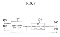
- FIG. 7 A conventionally known video signal processing device is shown in Fig. 7. This device synthesizes an interlaced video signal and a sub-picture according to the DVD standard (hereinafter referred to as “sub-picture”) or an on-screen display (hereinafter abbreviated as "OSD”), converts the interlaced video signal into a progressive video signal, and simultaneously outputs the progressive video signal and the interlaced video signal.
- sub-picture DVD standard
- OSD on-screen display
- Fig. 7 is a diagram showing a conventional video signal processing device.
- the video signal processing device shown in Fig. 7 has a terminal 101 for input of interlaced video signals, a terminal 102 for input of signals displaying a sub-picture or an OSD, a synthesis portion 103 for synthesizing the interlaced video signal that is input from the input terminal 101 and the signal displaying a sub-picture or an OSD that is input from the input terminal 102 , an IP conversion portion 104 for converting the interlaced synthetic video signal that is output from the synthesis portion 103 into a progressive video signal, an output terminal 105 for outputting the progressive video signal from the IP conversion portion 104 , and an output terminal 106 for outputting the synthetic video signal from the synthesis portion 103 .
- the synthesis portion 103 synthesizes the interlaced video signal that is input from the input terminal 101 and the interlaced signal displaying a sub-picture or an OSD that is input from the input terminal 102 , and outputs the synthetic video signal.
- the synthetic video signal is output from the output terminal 106 as an interlaced video signal.
- the synthetic video signal that is output from the synthesis portion 103 is input to the IP conversion portion 104 .
- the IP conversion portion 104 employs scan line interpolation to convert the interlaced synthetic video signal into a progressive video signal, and the progressive video signal is then output from the output terminal 105 .
- the interlaced video signal is synthesized with the signal displaying a sub-picture or an OSD before it is converted to a progressive video signal, and thus scan line interpolation causes the sub-picture or OSD image to become blurred. Therefore, the quality of the video image is deteriorated.
- the interlaced video image and the sub-picture are synthesized in the interlaced format. If synthesis is performed in the interlaced format and the display lines displaying the sub-picture are managed by the frame line numbers, then the line numbers must be converted to field line numbers. Consequently, the scale of the circuit becomes large.
- It is an object of the invention is provide a video signal processing device with which the picture quality is not deteriorated.
- a video signal processing device of the invention is provided with an IP conversion means for converting a first interlaced video signal, which has been input, into a first progressive video signal and outputting it, a synthesis means for synthesizing the first progressive video signal and a sub-video signal for displaying a sub-video that has been input and outputting the result as a second progressive video signal, and a PI conversion means for converting the second progressive video signal into a second interlaced video signal and outputting it, and the second progressive video signal and the second interlaced video signal are both output.
- the interlaced video signal is converted into a progressive video signal it is synthesized with the sub-video.
- a deterioration of the picture quality can be prevented without the sub-video becoming blurred.
- the sub-video is synthesized to a progressive video signal, it is not necessary to convert the line numbers to field line numbers, which allows the circuit scale to be kept small.
- the sub-video signal that is synthesized by the synthesis means is a signal for displaying a sub-picture or an on-screen display.
- the IP conversion means interpolates scan lines from the first interlaced video signal so as to convert the first interlaced video signal into the first progressive video signal and outputs the first progressive video signal, and that the PI conversion means decimates the scan lines that have been interpolated by the IP conversion means so as to convert the second progressive video signal into the second interlaced video signal and outputs the second interlaced video signal.
- the IP conversion means interpolates scan lines from the first interlaced video signal so as to convert the first interlaced video signal into the first progressive video signal and outputs the first progressive video signal, and outputs to the PI conversion means a field identification signal that indicates whether the first progressive video signal has been interpolated from scan lines of an odd-numbered field or an even-numbered field of the first interlaced video signal, and that the PI conversion means decimates even-numbered scan lines of the second progressive video signal and converts these to the second interlaced video signal if from the field identification signal it is determined that the first progressive video signal has been interpolated from scan lines of an odd-numbered field of the first interlaced video signal, and decimates odd-numbered scan lines of the second progressive video signal and converts these to the second interlaced video signal if from the field identification signal it is determined that the first progressive video signal has been interpolated from scan lines of an even-numbered field of the first interlaced video signal.
- another video signal processing device of the invention is provided with an IP conversion means for converting a first interlaced video signal, which has been input, into a first progressive video signal and outputting it, a synthesis means for synthesizing the first progressive video signal and a sub-video signal for displaying a sub-video that has been input and outputting the result as a second progressive video signal, a PI conversion means for converting the second progressive video signal into a second interlaced video signal and outputting it, and a field signal generation means for outputting a field identification signal that indicates whether a field of the second interlaced video signal from the PI conversion means is an odd-numbered field or an even-numbered field, and the second progressive video signal and the second interlaced video signal are both output.
- the interlaced video signal is converted into a progressive video signal it is synthesized with the sub-video.
- a deterioration of the picture quality can be prevented without the sub-video becoming blurred.
- the sub-video is synthesized to a progressive video signal, it is not necessary to convert the line numbers to field line numbers, which allows the circuit scale to be kept small.
- the sub-video signal that is synthesized by the synthesis means is a signal for displaying a sub-picture or an on-screen display.
- the IP conversion means interpolates scan lines from the first interlaced video signal so as to convert the first interlaced video signal into the first progressive video signal and outputs the first progressive video signal, and that the PI conversion means decimates the scan lines that have been interpolated by the IP conversion means so as to convert the second progressive video signal into the second interlaced video signal and outputs the second interlaced video signal.
- the IP conversion means in a case where the field identification signal received from the field signal generation means indicates an odd-numbered field, interpolates scan lines from an odd-numbered field of the first interlaced video signal so as to convert the first interlaced video signal into the first progressive video signal and outputs the first progressive video signal, and in a case where the field identification signal received from the field signal generation means indicates an even-numbered field, interpolates scan lines from an even-numbered field of the first interlaced video signal so as to convert the first interlaced video signal into the first progressive video signal and outputs the first progressive video signal, and that the PI conversion means decimates even-numbered scan lines of the second progressive video signal and converts these to the second interlaced video signal if the field identification signal received from the field signal generation means indicates an odd-numbered field, and decimates odd-numbered scan lines of the second progressive video signal and converts these to the second interlaced video signal if the field identification signal received from the field signal generation means indicates an even-numbered field.
- a yet further video signal processing device of the invention is provided with an IP conversion means for converting a first interlaced video signal, which has been input, into a first progressive video signal and outputting it, a synthesis means for synthesizing the first progressive video signal and a sub-video signal for displaying a sub-video that has been input and outputting the result as a second progressive video signal, a line memory for converting the second progressive video signal into the second interlaced video signal and outputting it, a progressive horizontal synchronizing pulse generation means for outputting a progressive horizontal synchronizing pulse signal based on a clock signal that is input, an interlaced horizontal synchronizing pulse generation means for outputting an interlaced horizontal synchronizing pulse signal based on the clock signal, a field signal generation means for outputting a field identification signal that indicates whether a field of the second interlaced video signal from the line memory is an odd-numbered field or an even-numbered field, based on the interlaced horizontal synchronizing pulse signal from the interlaced horizontal synchron
- the interlaced video signal is converted into a progressive video signal it is synthesized with the sub-video.
- a deterioration of the picture quality can be prevented without the sub-video becoming blurred.
- the sub-video is synthesized to a progressive video signal, it is not necessary to convert the line numbers to field line numbers, which allows the circuit scale to be kept small.
- the sub-video signal that is synthesized by the synthesis means is a signal for displaying a sub-picture or an on-screen display.
- the IP conversion means in a case where the field identification signal received from the field signal generation means indicates an odd-numbered field, interpolates scan lines from an odd-numbered field of the first interlaced video signal so as to convert the first interlaced video signal into the first progressive video signal and outputs the first progressive video signal, and in a case where the field identification signal received from the field signal generation means indicates an even-numbered field, interpolates scan lines from an even-numbered field of the first interlaced video signal so as to convert the first interlaced video signal into the first progressive video signal and outputs the first progressive video signal; that the write control means outputs the write control signal for writing the odd-numbered scan lines of the second progressive video signal to the line memory if the field identification signal from the field signal generation means indicates an odd-numbered field, and outputs the write control signal for writing the even-numbered scan lines of the second progressive video signal to the line memory if the field identification signal from the field signal generation means indicates an even-numbered field; and that the read control means
- Fig. 1 is a diagram showing a configuration example of the video signal processing device according to the first embodiment of the invention.
- the video signal processing device shown in Fig. 1 has an input terminal 1 , an input terminal 2 , an IP conversion portion 3 (corresponds to the IP conversion means), a synthesis portion 4 (corresponds to the synthesis means), a PI conversion portion 5 (corresponds to the PI conversion means), an output terminal 6 , and an output terminal 7 .
- the input terminal 1 is for input of an interlaced video signal S1 (corresponds to the first interlaced video signal).
- the input terminal 2 is for input of a signal S2 (corresponds to the sub-video signal) for displaying a sub-picture according to the DVD standard (hereinafter referred to as “sub-picture”) or an on-screen display (hereinafter abbreviated as "OSD").
- a signal S2 corresponds to the sub-video signal
- sub-picture a sub-picture according to the DVD standard
- OSD an on-screen display
- the IP conversion portion 3 converts the interlaced video signal S1 from the input terminal 1 into a progressive video signal S3 (corresponds to the first progressive video signal) using scan line interpolation, and outputs this signal. Moreover, the IP conversion portion 3 uses an internally provided identification portion 3a (not shown) to identify whether the progressive video signal S3 that is output is based on an interface video signal S1 on which scan line interpolation has been performed for the odd-numbered field or for the even-numbered field, and outputs to the PI conversion portion 5 an even/odd field identification signal S4 (corresponds to the field identification signal) indicating which of these fields have been subjected to scan line interpolation.
- an even/odd field identification signal S4 corresponds to the field identification signal
- the synthesis portion 4 synthesizes the progressive video signal S3 that is output from the IP conversion portion 3 and the signal S2 displaying a sub-picture or an OSD from the input terminal 2 , and outputs a progressive synthetic video signal S5 (corresponds to the second progressive video signal).
- the PI conversion portion 5 converts the progressive synthetic video signal S5 from the synthesis portion 4 into an interlaced video signal S6 (corresponds to the second interlaced video signal) based on the even/odd field identification signal S4 that is input from the IP conversion portion 3 .
- the output terminal 6 outputs the progressive synthetic video signal S5 from the synthesis portion 4 .
- the output terminal 7 outputs the interlaced video signal S6 from the PI conversion portion 5 .
- the interlaced video signal S1 that is input from the input terminal 1 is converted into the progressive video signal S3 by the IP conversion portion 3 through scan line interpolation (described in detail later). Then, the synthesis portion 4 synthesizes the progressive video signal S3 and the signal S2 displaying a sub-picture or an OSD from the input terminal 2 , and outputs the synthetic video signal S5 .
- the synthetic video signal S5 from the synthesis portion 4 is output from the output terminal 6 .
- the progressive synthetic video signal S5 from the synthesis portion 4 is converted to the interlaced video signal S6 by the PI conversion portion 5 (explained in detail later), and is output from the output terminal 7 .
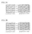
- Fig. 2 is a diagram for illustrating an example of conversion from the interlaced video signal S1 to the progressive video signal S3 .
- Fig. 2A is a diagram for describing an example of conversion in which the interlaced video signal S1 that is input to the IP conversion portion 3 is an odd-numbered field.
- Fig. 2B is a diagram for describing an example of conversion in which the interlaced video signal S1 that is input to the IP conversion portion 3 is an even-numbered field.
- the IP conversion portion 3 outputs the interlaced video signal S1 as the odd-numbered scan lines of the progressive video signal S3 .
- the IP conversion portion 3 outputs the interlaced video signal S1 as the odd-numbered scan lines of the progressive video signal S3 at twice the speed at which the interlaced video signal S1 is input.
- the even-numbered scan lines of the progressive video signal S3 are interpolated from the scan lines before and after the lines of the interlaced video signal S1 , and are output.
- the IP conversion portion 3 outputs an L-level even/odd field identification signal S4 .
- the IP conversion portion 3 outputs the interlaced video signal S1 as the even-numbered scan lines of the progressive video signal S3 .
- the IP conversion portion 3 outputs the interlaced video signal S1 as the even-numbered scan lines of the progressive video signal S3 at twice the speed at which the interlaced video signal S1 is input.
- the odd-numbered scan lines of the progressive video signal S3 are interpolated from the scan lines before and after the lines of the interlaced video signal S1 , and are output.
- the IP conversion portion 3 outputs an H-level even/odd field identification signal S4 .
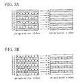
- Fig. 3 is a diagram for explaining examples of conversion from the progressive synthetic video signal S5 to the interlaced video signal S6 .
- Fig. 3A is a diagram for illustrating an example of conversion when the even/odd identification signal S4 that is input to the PI conversion portion 5 is L-level
- Fig. 3B is a diagram for illustrating an example of conversion when the even/odd field identification signal S4 that is input to the PI conversion portion 5 is H-level.
- the PI conversion portion 5 outputs the odd-numbered scan lines of the progressive synthetic video signal S5 that has been input to serve as the interlaced video signal S6 , and does not output the even-numbered scan lines. Also, the output of the odd-numbered scan lines is made at half the speed at which the synthetic video signal S5 is input to the PI conversion portion 5.
- the PI conversion portion 5 outputs the even-numbered scan lines of the progressive synthetic video signal S5 that has been input to serve as the interlaced video signal S6 , and does not output the odd-numbered scan lines. Also, the output of the even-numbered scan lines is made at half the speed at which the synthetic video signal S5 is input to the PI conversion portion 5 .
- the interlaced video signal S6 that is output from the PI conversion portion 5 becomes a signal equivalent to the interlaced video signal S1 that is input to the input terminal 1 .
- the PI conversion portion 5 outputs half the number of the scan lines of the progressive synthetic video signal S5 that is input at half the speed at which the progressive synthetic video signal S5 is input, no time difference occurs between the progressive synthetic video signal S5 that is input and the interlaced video signal S6 that is output. To put it differently, no time difference occurs between the progressive synthetic video signal S5 that is output from the output terminal 6 and the interlaced video signal S6 that is output from the output terminal 7 .
- a sub-picture or an OSD serves as the video that is synthesized to the first progressive video signal S3 , however, the present invention is not limited to this, and the invention can be similarly embodied even if a video used as a sub-video is displayed.
- the video signal processing device synthesizes the interlaced video signal S1 that is input and the signal S2 that displays a sub-picture or an OSD after the interlaced video signal S1 has been converted to the progressive video signal S3 .
- the progressive synthetic video signal S5 that is output from the output terminal 6 does not exhibit a blurred sub-picture or OSD image due to scan line interpolation, which allows the picture quality to be kept from deteriorating.
- the sub-picture is synthesized to the progressive video signal S3 , it is no longer necessary to convert the display lines displaying the sub-picture, which is managed by frame line numbers, to field line numbers, and thus the scale of the circuit can be kept small.
- the interlaced video signal S1 that is input from the input terminal 1 and the interlaced video signal S6 that is output from the output terminal 7 are equivalent signals, and thus deterioration of picture quality due to the interlaced video signal S6 can be prevented. Also, as mentioned above, no time difference occurs between the progressive synthetic video signal S5 that is output from the output terminal 6 and the interlaced video signal S6 that is output from the output terminal 7 .
- Fig. 4 is a diagram showing an example of the configuration of the video signal processing device according to a second embodiment of the invention.
- the video signal processing device shown in Fig. 4 has an input terminal 1 , an input terminal 2 , an IP conversion portion 13 (corresponds to the IP conversion means), a synthesis portion 4 (corresponds to the synthesis means), a PI conversion portion 5 (corresponds to the PI conversion means), a field signal generation portion 18 (corresponds to the field signal generation means), an output terminal 6 , and an output terminal 7 .
- the input terminal 1 is for input of an interlaced video signal S1 (corresponds to the first interlaced video signal).
- the input terminal 2 is for input of a signal S2 (corresponds to the sub-video signal) displaying a sub-picture or an OSD.
- the IP conversion portion 13 converts the interlaced video signal S1 from the input terminal 1 into a progressive video signal S3 (corresponds to the first progressive video signal) through scan line interpolation based on a later-described even/odd field identification signal S4 that is input from the field signal generation portion 18 , and outputs this signal.
- the synthesis portion 4 synthesizes the progressive video signal S3 that is output from the IP conversion portion 13 and the signal S2 displaying a sub-picture or an OSD from the terminal 2 , and outputs a progressive synthetic video signal S5 (corresponds to the second progressive video signal).
- the PI conversion portion 5 converts the progressive synthetic video signal S5 from the synthesis portion 4 into an interlaced video signal S6 (corresponds to the second interlaced video signal) based on the later-described even/odd field identification signal S4 that is input from the field signal generation portion 18 .
- the field signal generation portion 18 outputs the even/odd field identification signal S4 (corresponds to the field identification signal), which indicates whether the interlaced video signal S6 that is output from the PI conversion portion 5 is an odd-numbered field or an even-numbered field.
- the field signal generation portion 18 outputs an L-level even/odd field identification signal S4 in the case of an odd-numbered field, and outputs an H-level even/odd field identification signal S4 in the case of an even-numbered field.
- the output terminal 6 outputs the progressive synthetic video signal S5 from the synthesis portion 4 .
- the output terminal 7 outputs the interlaced video signal S6 from the PI conversion portion 5 .
- the interlaced video signal S1 that is input from the input terminal 1 is converted into the progressive video signal S3 through scan line interpolation by the IP conversion portion 13 (described in detail later). Then, the synthesis portion 4 synthesizes the progressive video signal S3 and the signal S2 displaying a sub-picture or an OSD from the input terminal 2 , and outputs the synthetic video signal S5 .
- the synthetic video signal S5 from the synthesis portion 4 is output from the output terminal 6 .
- the progressive synthetic video signal S5 from the synthesis portion 4 is converted into the interlaced video signal S6 by the PI conversion portion 5 based on the even/odd field identification signal S4 , and is output from the output terminal 7 .
- the IP conversion portion 13 outputs the interlaced video signal S1 as odd-numbered scan lines of the progressive video signal S3 .
- the IP conversion portion 13 outputs the interlaced video signal S1 as odd-numbered scan lines of the progressive video signal S3 at twice the speed at which the interlaced video signal S1 is input.
- the even-numbered scan lines of the progressive video signal S3 are interpolated from the scan lines before and after the lines of the interlaced video signal S1 and are output.
- the IP conversion portion 13 outputs the interlaced video signal S1 as even-numbered scan lines of the progressive video signal S3 .
- the IP conversion portion 13 outputs the interlaced video signal S1 as even-numbered scan lines of the progressive video signal S3 at twice the speed at which the interlaced video signal S1 is input.
- the odd-numbered scan lines of the progressive video signal S3 are interpolated from the scan lines before and after the lines of the interlaced video signal S1 and are output.
- the operation of the PI conversion portion 5 is the same as described in the first embodiment, and thus description thereof is omitted.
- the even/odd field identification signal S4 is generated by the field signal generation portion 18 , and thus the device of this embodiment differs from the device of the first embodiment only in that the means for generating the even/odd field identification signal S4 are different. Therefore, the device of this embodiment exhibits the same effects as the device of the first embodiment.
- Fig. 5 is a diagram showing an example of the configuration of the video signal processing device according to the third embodiment of the invention.
- the video signal processing device shown in Fig. 5 has an input terminal 1 , an input terminal 2 , an IP conversion portion 13 (corresponds to the IP conversion means), a synthesis portion 4 (corresponds to the synthesis means), a line memory 21 , a write control portion 22 (corresponds to the write control means), a read control portion 23 (corresponds to the read control means), an HP generation portion 24 (corresponds to the progressive horizontal synchronizing pulse generation means), an HI generation portion 25 (corresponds to the interlaced horizontal synchronizing pulse generation means), a field signal generation portion 26 (corresponds to the field signal generation means), a clock input terminal 27 , an output terminal 6 , and an output terminal 7 .
- the HP generation portion 24 generates a progressive-type horizontal synchronizing pulse signal S22 (hereinafter referred to as "progressive horizontal synchronizing pulse signal”) from a clock signal S21 received from the clock input terminal 27 , and outputs it.
- a progressive-type horizontal synchronizing pulse signal S22 hereinafter referred to as "progressive horizontal synchronizing pulse signal”
- the HI generation portion 25 generates an interlaced-type horizontal synchronizing pulse signal S23 (hereinafter referred to as "interlaced horizontal synchronizing pulse signal”) from the clock signal S21 received from the clock input terminal 27 , and outputs it.
- interlaced horizontal synchronizing pulse signal an interlaced-type horizontal synchronizing pulse signal
- the field signal generation portion 26 outputs the even/odd field identification signal S4 (corresponds to the field identification signal), which indicates whether the interlaced video signal S6 that is output from the line memory 21 is an odd-numbered field or an even-numbered field, based on the interlaced horizontal synchronizing pulse signal S23 from the HI generation portion 25 .
- the field signal generation portion 26 outputs an L-level even/odd field identification signal S4 in the case of an odd-numbered field and outputs an H-level even/odd field identification signal S4 in the case of an even-numbered field.
- the write control portion 22 outputs a write control signal S24 to the line memory 21 based on the progressive horizontal synchronizing pulse signal S22 from the HP generation portion 24 and the even/odd field identification signal S4 .
- the read control portion 23 outputs a read control signal S25 to the line memory 21 based on the interlaced horizontal synchronizing pulse signal S23 from the HI generation portion 25 and the even/odd field identification signal S4 .
- the interlaced video signal S1 (corresponds to the first interlaced video signal) that is input from the input terminal 1 is converted into the progressive video signal S3 (corresponds to the first progressive video signal) through scan line interpolation by the IP conversion portion 13 .
- the synthesis portion 4 synthesizes the progressive video signal S3 and the signal S2 displaying a sub-picture or an OSD from the input terminal 2 , and outputs the synthetic video signal S5 (corresponds to the second progressive video signal).
- the synthetic video signal S5 from the synthesis portion 4 is output from the output terminal 6 .
- the progressive synthetic video signal S5 from the synthesis portion 4 is written into the line memory 21 .
- the video signal that is read out from the line memory is output from the output terminal 7 as the interlaced video signal S6 (corresponds to the second interlaced video signal).
- Fig. 6 is a diagram for illustrating examples of conversion from the progressive synthetic video signal S5 to the interlaced video signal S6 using the line memory 21 , the write control portion 22 , and the read control portion 23 .
- Fig. 6A is a diagram for illustrating the operation when the even/odd field identification signal S4 is L-level
- Fig. 6B is a diagram for illustrating the operation when the even/odd field identification signal S4 is H-level. It should be noted that N in Fig. 6 is an integer.
- the write control signal S24 that is generated from the progressive horizontal synchronizing pulse signal S22 is H-level only when the progressive synthetic video signal S5 is an odd-numbered line, and during the period that the write control signal S24 is H-level the progressive video signal S5 is written into the line memory 21 . Then, during the period that the read control signal S25 generated from the interlaced horizontal synchronizing pulse signal S23 is H-level, the interlaced video signal S6 is read out at half the speed of the synthetic video signal S5 .
- the write control signal S24 that is generated from the progressive horizontal synchronizing pulse signal S22 is H-level only when the progressive synthetic video signal S5 is an even-numbered line, and during the period that the write control signal S24 is H-level the progressive video signal S5 is written into the line memory 21 . Then, during the period that the read control signal S25 generated from the interlaced horizontal synchronizing pulse signal S23 is H-level, the interlaced video signal S6 is read out at half the speed of the synthetic video signal S5 .
- the interlaced video signal S6 that is output from the line memory 21 becomes a signal equivalent to the interlaced video signal S1 that is input to the input terminal 1 .
- the line memory 21 outputs half the number of the scan lines of the input progressive synthetic video signal S5 at half the speed at which the progressive synthetic video signal S5 is input, no time difference occurs between the progressive synthetic video signal S5 that is input and the interlaced video signal S6 that is output. To put it differently, no time difference occurs between the progressive synthetic video signal S5 that is output from the output terminal 6 and the interlaced video signal S6 that is output from the output terminal 7 .
- the video signal processing device is capable of achieving the same effects as the devices of the first and the second embodiments.
- the sub-picture or the OSD is synthesized after the interlaced video signal has been converted into a progressive video signal, and thus a blurred sub-picture or OSD image caused by scan line interpolation can be eliminated and the picture quality can be kept from deteriorating. Also, by decimating the scan lines that have been interpolated in the conversion from the interlaced video signal to a progressive video signal, a deteriorated picture quality due to the output of an interlaced video signal can be prevented.
Applications Claiming Priority (2)
| Application Number | Priority Date | Filing Date | Title |
|---|---|---|---|
| JP2002152749A JP2003348446A (ja) | 2002-05-27 | 2002-05-27 | 映像信号処理装置 |
| JP2002152749 | 2002-05-27 |
Publications (2)
| Publication Number | Publication Date |
|---|---|
| EP1367820A2 true EP1367820A2 (de) | 2003-12-03 |
| EP1367820A3 EP1367820A3 (de) | 2007-08-29 |
Family
ID=29417155
Family Applications (1)
| Application Number | Title | Priority Date | Filing Date |
|---|---|---|---|
| EP03011225A Withdrawn EP1367820A3 (de) | 2002-05-27 | 2003-05-16 | Videosignalsverarbeitungsvorrichtung |
Country Status (6)
| Country | Link |
|---|---|
| US (1) | US20030218692A1 (de) |
| EP (1) | EP1367820A3 (de) |
| JP (1) | JP2003348446A (de) |
| KR (1) | KR20030091804A (de) |
| CN (1) | CN1257645C (de) |
| TW (1) | TWI266532B (de) |
Cited By (1)
| Publication number | Priority date | Publication date | Assignee | Title |
|---|---|---|---|---|
| EP1619886A1 (de) * | 2004-07-22 | 2006-01-25 | Harman Becker Automotive Systems GmbH | Videoformatanpassung |
Families Citing this family (6)
| Publication number | Priority date | Publication date | Assignee | Title |
|---|---|---|---|---|
| JP4395778B2 (ja) * | 2003-04-09 | 2010-01-13 | パナソニック株式会社 | Osd合成画像復号装置、osd合成画像復号方法、プログラム、記録媒体 |
| EP1741282A1 (de) * | 2004-04-30 | 2007-01-10 | Nvidia Corporation | Verfahren und vorrichtung zur vertikalen skalierung von pixeldaten |
| JP2006129069A (ja) * | 2004-10-28 | 2006-05-18 | Canon Inc | 撮像装置及び撮像方法 |
| JP4933209B2 (ja) * | 2006-10-05 | 2012-05-16 | パナソニック株式会社 | 映像処理装置 |
| JP5023805B2 (ja) * | 2007-05-16 | 2012-09-12 | ソニー株式会社 | 画像処理装置および画像処理方法、並びにプログラム |
| US20080291323A1 (en) * | 2007-05-22 | 2008-11-27 | Seiko Epson Corporation | Image processing device, data recording device, and method of controlling image processing device |
Citations (4)
| Publication number | Priority date | Publication date | Assignee | Title |
|---|---|---|---|---|
| US5327156A (en) * | 1990-11-09 | 1994-07-05 | Fuji Photo Film Co., Ltd. | Apparatus for processing signals representative of a computer graphics image and a real image including storing processed signals back into internal memory |
| US5777683A (en) * | 1995-05-08 | 1998-07-07 | Medison Co., Ltd. | Ultrasonic imaging system adopting a non-interlaced scanning method |
| US6041142A (en) * | 1993-12-02 | 2000-03-21 | General Instrument Corporation | Analyzer and methods for detecting and processing video data types in a video data stream |
| JP2001103434A (ja) * | 1999-08-23 | 2001-04-13 | Samsung Electronics Co Ltd | 走査方式変換装置及びその方法 |
Family Cites Families (10)
| Publication number | Priority date | Publication date | Assignee | Title |
|---|---|---|---|---|
| US5325131A (en) * | 1993-05-03 | 1994-06-28 | Tektronix, Inc. | Multiformat television switcher |
| US5530484A (en) * | 1995-05-19 | 1996-06-25 | Thomson Multimedia S.A | Image scanning format converter suitable for a high definition television system |
| US5963261A (en) * | 1996-04-29 | 1999-10-05 | Philips Electronics North America Corporation | Low cost scan converter for television receiver |
| JP3514063B2 (ja) * | 1997-02-20 | 2004-03-31 | 松下電器産業株式会社 | 受信装置 |
| US6798458B1 (en) * | 1998-10-01 | 2004-09-28 | Matsushita Electric Industrial Co., Ltd. | Image signal conversion equipment |
| JP2001203988A (ja) * | 2000-01-21 | 2001-07-27 | Nec Corp | 画像復号装置、半導体装置、及び画像復号方法 |
| JP2001231016A (ja) * | 2000-02-15 | 2001-08-24 | Matsushita Electric Ind Co Ltd | 映像信号再生装置 |
| US6927801B2 (en) * | 2000-11-20 | 2005-08-09 | Victor Company Of Japan, Ltd. | Video signal processing apparatus and video displaying apparatus |
| US7012648B2 (en) * | 2001-04-02 | 2006-03-14 | Matsushita Electric Industrial Co., Ltd. | Image conversion method and image conversion apparatus |
| US6573941B1 (en) * | 2002-04-22 | 2003-06-03 | Thomson Licensing Sa | Low bit rate compression format conversion for improved resolution |
-
2002
- 2002-05-27 JP JP2002152749A patent/JP2003348446A/ja not_active Withdrawn
-
2003
- 2003-04-14 US US10/412,392 patent/US20030218692A1/en not_active Abandoned
- 2003-05-16 EP EP03011225A patent/EP1367820A3/de not_active Withdrawn
- 2003-05-19 CN CNB031362346A patent/CN1257645C/zh not_active Expired - Fee Related
- 2003-05-27 TW TW092114232A patent/TWI266532B/zh not_active IP Right Cessation
- 2003-05-27 KR KR10-2003-0033538A patent/KR20030091804A/ko not_active Application Discontinuation
Patent Citations (4)
| Publication number | Priority date | Publication date | Assignee | Title |
|---|---|---|---|---|
| US5327156A (en) * | 1990-11-09 | 1994-07-05 | Fuji Photo Film Co., Ltd. | Apparatus for processing signals representative of a computer graphics image and a real image including storing processed signals back into internal memory |
| US6041142A (en) * | 1993-12-02 | 2000-03-21 | General Instrument Corporation | Analyzer and methods for detecting and processing video data types in a video data stream |
| US5777683A (en) * | 1995-05-08 | 1998-07-07 | Medison Co., Ltd. | Ultrasonic imaging system adopting a non-interlaced scanning method |
| JP2001103434A (ja) * | 1999-08-23 | 2001-04-13 | Samsung Electronics Co Ltd | 走査方式変換装置及びその方法 |
Cited By (1)
| Publication number | Priority date | Publication date | Assignee | Title |
|---|---|---|---|---|
| EP1619886A1 (de) * | 2004-07-22 | 2006-01-25 | Harman Becker Automotive Systems GmbH | Videoformatanpassung |
Also Published As
| Publication number | Publication date |
|---|---|
| EP1367820A3 (de) | 2007-08-29 |
| TWI266532B (en) | 2006-11-11 |
| CN1257645C (zh) | 2006-05-24 |
| CN1463145A (zh) | 2003-12-24 |
| TW200400760A (en) | 2004-01-01 |
| KR20030091804A (ko) | 2003-12-03 |
| JP2003348446A (ja) | 2003-12-05 |
| US20030218692A1 (en) | 2003-11-27 |
Similar Documents
| Publication | Publication Date | Title |
|---|---|---|
| KR100255907B1 (ko) | 영상신호 변환장치와 텔레비젼신호처리장치 | |
| US20050001929A1 (en) | Video signal converting apparatus and method | |
| US6040868A (en) | Device and method of converting scanning pattern of display device | |
| EP1367820A2 (de) | Videosignalsverarbeitungsvorrichtung | |
| JPH09307832A (ja) | 画面比変換装置及び方法 | |
| JPH04299687A (ja) | テレビジョン方式変換装置 | |
| US6417887B1 (en) | Image display processing apparatus and method for converting an image signal from an interlaced system to a progressive system | |
| KR950009698B1 (ko) | 엔티에스씨/에치디티브이(ntsc/hdtvm) 듀얼 리시버의 라인 트리플러 | |
| US20080136966A1 (en) | Frame Synchronizer, Synchronization Method of Frame Synchronizer, Image Processing Apparatus, and Frame Synchronization Program | |
| KR100403692B1 (ko) | 화상표시장치 | |
| US20040263688A1 (en) | Television receiver and control method thereof | |
| JP5225068B2 (ja) | 画像処理装置及び画像処理方法 | |
| US20100284672A1 (en) | Video signal processing method, integrated circuit, and video reproducer | |
| JP3259628B2 (ja) | 走査線変換装置 | |
| EP1458189A2 (de) | Videosignalverarbeitungsvorrichtung | |
| JP2001036871A (ja) | 画像供給装置および画像表示装置 | |
| JP2970592B2 (ja) | 映像処理方法 | |
| KR100343374B1 (ko) | 영상 신호 처리 장치 및 그 처리 방법 | |
| JP5207866B2 (ja) | 映像信号処理方法、映像信号処理装置 | |
| JP2001155673A (ja) | 走査型電子顕微鏡 | |
| JP2687346B2 (ja) | 映像処理方法 | |
| KR100706994B1 (ko) | 디인터레이싱 출력을 위한 필드단위의 프레임율 변환방법및 장치 | |
| JP5875422B2 (ja) | 画像処理装置及び画像処理装置の制御方法 | |
| JPH03505275A (ja) | 制御信号生成装置および方法 | |
| US20050046742A1 (en) | Image signal processing circuit |
Legal Events
| Date | Code | Title | Description |
|---|---|---|---|
| PUAI | Public reference made under article 153(3) epc to a published international application that has entered the european phase |
Free format text: ORIGINAL CODE: 0009012 |
|
| AK | Designated contracting states |
Kind code of ref document: A2 Designated state(s): AT BE BG CH CY CZ DE DK EE ES FI FR GB GR HU IE IT LI LU MC NL PT RO SE SI SK TR |
|
| AX | Request for extension of the european patent |
Extension state: AL LT LV MK |
|
| PUAL | Search report despatched |
Free format text: ORIGINAL CODE: 0009013 |
|
| AK | Designated contracting states |
Kind code of ref document: A3 Designated state(s): AT BE BG CH CY CZ DE DK EE ES FI FR GB GR HU IE IT LI LU MC NL PT RO SE SI SK TR |
|
| AX | Request for extension of the european patent |
Extension state: AL LT LV MK |
|
| AKX | Designation fees paid | ||
| STAA | Information on the status of an ep patent application or granted ep patent |
Free format text: STATUS: THE APPLICATION IS DEEMED TO BE WITHDRAWN |
|
| 18D | Application deemed to be withdrawn |
Effective date: 20080301 |
|
| REG | Reference to a national code |
Ref country code: DE Ref legal event code: 8566 |