EP1361718B1 - Pulsübertragungsmodulations- und -demodulationsverfahren - Google Patents
Pulsübertragungsmodulations- und -demodulationsverfahren Download PDFInfo
- Publication number
- EP1361718B1 EP1361718B1 EP03076282A EP03076282A EP1361718B1 EP 1361718 B1 EP1361718 B1 EP 1361718B1 EP 03076282 A EP03076282 A EP 03076282A EP 03076282 A EP03076282 A EP 03076282A EP 1361718 B1 EP1361718 B1 EP 1361718B1
- Authority
- EP
- European Patent Office
- Prior art keywords
- signal
- level
- modulated
- signals
- modulation
- Prior art date
- Legal status (The legal status is an assumption and is not a legal conclusion. Google has not performed a legal analysis and makes no representation as to the accuracy of the status listed.)
- Expired - Lifetime
Links
Images



Classifications
-
- H—ELECTRICITY
- H04—ELECTRIC COMMUNICATION TECHNIQUE
- H04L—TRANSMISSION OF DIGITAL INFORMATION, e.g. TELEGRAPHIC COMMUNICATION
- H04L25/00—Baseband systems
- H04L25/38—Synchronous or start-stop systems, e.g. for Baudot code
- H04L25/40—Transmitting circuits; Receiving circuits
- H04L25/49—Transmitting circuits; Receiving circuits using code conversion at the transmitter; using predistortion; using insertion of idle bits for obtaining a desired frequency spectrum; using three or more amplitude levels ; Baseband coding techniques specific to data transmission systems
- H04L25/4902—Pulse width modulation; Pulse position modulation
Definitions
- the present invention generally relates to a digital signal modulation and demodulation method used for transmission of digital signals.
- an original signal is modulated with a clock signal into a pulse-like modulated signal on the transmitting side, and this modulated signal being transmitted is received on the receiving side in a so-called self-synchronization method.
- the receiving side calculates the original clock information from the modulated signal and generates a clock signal in synchronization with the original clock for demodulation of the modulated signal to extract the original digital signal.
- modulation performed in combination of a clock signal and data for example, frequency modulation and phase modulation are known (refer, for example, to Japanese Laid-Open Patent Publication No. 2001-168723).
- signals In a case where signals must be sent at a high speed, for example, by a long-distance signal transmission or an insulated data transmission, or in a data transmission over an optical fiber, signals must be amplified to compensate the attenuation and to adjust the amplitude of the signals. If the signals are transmitted in pulses, they include direct current (DC) components, which condition makes it difficult to amplify signal changes at a large scale. Therefore, in this case, it is necessary to adopt a receiving circuit with a large amplification receiver which is connected to an alternating current (AC).
- DC direct current
- the modulation on the transmitting side can be executed by a circuit simply constructed with a clock element.
- the demodulation on the receiving side can be executed by a simple circuit which receives the modulated signal, delays it by a predetermined delay time and uses this delayed signal as a clock signal for the demodulation. Therefore, transmitter-receiver devices that use the digital signal modulation and demodulation method according to the present invention can be manufactured inexpensively in a miniaturized fashion.
- the modulated signals comprise pulse signals having a duty ratio (H : L) of 1 : 3 and 3 : 1 or 3 : 1 and 1 : 3 in correspondence to the H level and the L level of the digital signal.
- digital signals are modulated with a clock signal to modulated signals, which are pulse signals having duty ratios (H : L) of 1 : N and N : 1 (with N > 1).
- N is preferably minimized to improve the efficiency of modulation and the transmission efficiency of the modulated signals.
- pulse signals having duty ratios (H : L) of 2 : 1 and 1 : 2 are expressed in three ways.
- modulation must be executed in states that are expressed by use of three clock periods of the clock signal, i.e., six states.
- N if N equals 3, then pulse signals having duty ratios (H : L) of 3 : 1 and 1 : 3 are expressed in four ways.
- modulation can be executed in states that are expressed by use of two clock periods of the clock signal, i.e., four states, and the clock signal is used efficiently for the modulation. Therefore, in the following description, modulated signals are arranged as pulse signals having duty ratios (H : L) of 3 : 1 and 1 : 3.
- the modulated signals that correspond to the logic H level of the data signals are expressed as pulse signals with a duty ratio (H : L) of 3 : 1 while those corresponding to the logic L level of the data signals are expressed as pulse signals with a duty ratio (H : L) of 1 : 3.
- these modulated signals may be expressed as pulse signals with duty ratios of 1 : 3 and 3 : 1, respectively, to achieve the same effect.
- a digital circuit performs signal processing in steps, using a clock signal, and the logic values (0 and 1) of the data signals are represented as the H level signals or the L level signals in synchronization to the clock signal.
- the frequency of the modulating clock signal is even times (twice or more) that of the data signals.
- the data signals are modulated into the modulated signals as pulse signals having duty ratios (H : L) of 3 : 1 and 1 : 3.
- Tm 2T
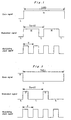
- part of the data signal at the L level for time period Td(L) is modulated by the modulating clock signal with period T and output as a multiple of modulated signals each having a duty ratio (H : L) of 1 : 3 and a period of Tm as shown in FIG. 2.
- the duty ratios of the modulated signals that correspond to the respective H and L levels of the data signal in modulation may be exactly opposite of that described above as mentioned previously.
- the preferred embodiment uses an alternating current amplifier to amplify the alternating current components of the modulated signals, the alternating current components being those components alternating around the direct current components (direct current levels) included in the modulated signals.
- the modulated signals comprise pulse waves that oscillate up and down around the part at 50% of the amplitude of the modulated signals (this part is referred to as the "ideal direct current level").
- the direct current component (direct current level) of the modulated signals is 75% of the amplitude as shown in FIG. 3.
- the direct current component (direct current level) is 25% of the amplitude as shown in FIG. 4.
- the alternating current components of the modulated signals i.e., the upward or downward amplitude of the direct current components
- a saturation amplifier can be used for the amplification of the modulated signals.
- demodulation is executed for modulated signals that have been modulated as pulse signals each having a duty ratio (H : L) of 3 : 1 in which the data signal at the H level repeats with a period of Tm and also for modulated signals that have been modulated as pulse signals each having a duty ratio (H : L) of 1 : 3 in which the data signal at the L level repeats with a period of Tm.
- the signal at the predetermined delay time Ty after the signal change from the L level to the H level is at the H level as shown in FIG. 5. Therefore, this signal with period Tm is converted to a signal with the H level.
- the modulated signals with a duty ratio (H : L) of 3 : 1 persist, the H level continues in the data signal being demodulated as shown in the drawing.
- the H level of the data signal having existed prior to the modulation is reproduced accurately in the demodulation.
- the signal at the predetermined delay time Ty after the signal change from the L level to the H level is at the L level as shown in FIG. 6. Therefore, this signal with period Tm is converted to a signal with the L level.
- the modulated signals with a duty ratio (H : L) of 1 : 3 persist, the L level continues in the data signal being demodulated as shown in the drawing.
- the predetermined delay time Ty the L level of the data signal having existed prior to the modulation is reproduced accurately in the demodulation.
- a D flip-flop For the extraction of the data signals by demodulating the modulated signals as described above, for example, a D flip-flop is used.
- the modulated signals are put into the D-input terminal of the D flip-flop while also the modulated signals delayed by the predetermined delay time Ty are put into the clock-input terminal thereof, to generate the demodulated data signals from the Q-output terminal of the D flip-flop.
- the D flip-flop is a flip-flop that picks up the condition of the signal being fed into the D-input when the signal level fed into the clock-input rises and that expresses the condition as output from the Q-output terminal thereof.
- the modulated signals delayed by the predetermined time and fed into the clock-input of the D flip-flop enable the D flip-flop to reproduce the original signals (data signals) in the demodulation.
- the delay time Ty for the modulated signals to be fed into the clock-input terminal must satisfy the following condition: Ty ⁇ (3/4)Tm.
- Ty ⁇ (3/4)Tm As it is apparent from FIG. 5, if the delay time Ty is too long with respect to the period of the modulated signals having a duty ratio (H : L) of 3 : 1 and allows the signal level at the delay time
- the delay time Ty must also satisfy the following condition: Ty > (1/4)Tm.
- Ty (1/4)Tm.
- the delay time Ty is too short with respect to the period of the modulated signals having a duty ratio (H : L) of 1 : 3 and allows the signal level at the delay time Ty to remain at the H level, then the demodulation does not reproduce the correct data signals, either. Therefore, the following conditional expression (2) must be satisfied. (1/4)Tm ⁇ Ty ⁇ (3/4)Tm
- the delay time Ty must satisfy the following conditional expression (3). ⁇ 1/(N+1) ⁇ Tm ⁇ Ty ⁇ ⁇ N/(N+1) ⁇ Tm
- the digital signal modulation and demodulation method according to the present invention can simplify the construction of the modulation and demodulation device because, for the demodulation of the modulated signals, it does not require the extraction from the modulated signals of the modulating clock information that has been used for the modulation of the data signals.
- FIG. 9 shows waveforms, which are labeled, respectively, with circled numbers that correspond to the identical numbers of points in FIG. 7 where these waveforms are observed.
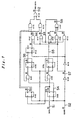
- flip-flop U101 functions to set the delay time of a data signal S1 to a modulating clock signal S2 and outputs a signal S3 which is synchronized with the modulating clock signal S2 and an inverse logic signal S4.
- Gate element U103 and flip-flop U104 constitute a toggle counter, in which each element alternately uses the clock pulses of the modulating clock signal S2 while signal S3 is at the H level.
- the toggle counter outputs a signal S5 which alternates between the H level and the L level, the time of the signal staying at each level corresponding to the period of the modulating clock signal S2.
- another gate element U105 and another flip-flop U106 constitute another toggle counter, in which each element also alternately uses the clock pulses of the modulating clock signal S2 while signal S3 is at the L level, i.e., while the inverse logic signal S4 of signal S3 is at the H level.
- this toggle counter outputs a signal S6 which alternates between the H level and the L level, the time of the signal staying at each level corresponding to the period of the modulating clock signal S2.
- flip-flop U104 is being toggled in synchronization with the modulating clock signal S2 while the output S3 of flip-flop U101 is at the H level.
- the signal S5 being output alternates between the H level and the L level, each level lasting for the corresponding period of the modulating clock signal S2.
- the modulating clock signal S2 has a frequency even-times that of the data signal S1
- the flip-flop resumes the original toggle condition when the toggling stops.
- Gate element U118 is used for alleviating the effect of delay time, etc. of components which constitute the circuit. It outputs a modulating clock signal S7 which is adjusted from the modulating clock signal S2. If the delay time of components constituting the circuit is substantially short with respect to the period of the modulating clock signal S2, then this gate element may be omitted, and the circuit will be still functionable at an equivalent performance.
- Gate elements U108, U109, U110 and U107 constitute a set-reset flip-flop, which receives the signal S5 output from flip-flop U104 and the modulating clock signal S7 adjusted by gate element U118.
- the set-reset flip-flop comprises the same number of gate elements as the number of steps to make the signal delay time evenly distributed. However, if the delay time of the set-reset flip-flop is substantially short with respect to the period of the adjusted modulating clock signal S7, then gate element U110 may be omitted, and the set-reset flip-flop may be still functionable at an equivalent performance.
- the set-reset flip-flop outputs a signal S8 which keeps the H level for a period from a rise of the adjusted modulating clock signal S7 to the next rise thereof and feeds this signal S8 to gate element U111.
- this gate element U111 outputs a signal S9 which has a modulated pulse extending at the H level over a period that corresponds to the H level, L level and H level of the clock signal S7.
- signal S9 is the modulated signal (a pulse signal with a duty ratio (H : L) of 3 : 1) for the data signal S 1 at the H level.
- gate element U105 receives a signal S4 at the H level, which is the inverse logic of signal S3 at the L level.
- the L level of the data signal S 1 is taken at time T4 and is output in synchronization with the modulating clock signal S2.
- Flip-flop U106 is being toggled in synchronization with the modulating clock signal S2 while the output S3 of flip-flop U101 is at the L level, i.e., while the inverse logic S4 of signal S3 is at the H level.
- the signal S6 being output from the flip-flop alternates between the H level and the L level, each level lasting for the corresponding period of the modulating clock signal S2.
- the modulating clock signal S2 has a frequency even-times that of the data signal S1, the flip-flop resumes the original toggle condition when the toggling stops.
- Gate element U119 and flip-flop U112 are used for synchronization to the fall of the adjusted modulating clock signal S7 to switch the H level of the modulating clock signal S7 without the effect of delay time, etc. of components which constitute the circuit. However, if the delay time of components constituting the circuit is substantially short with respect to the period of the adjusted modulating clock signal S7, then these elements may be omitted, and the circuit may be still functionable at an equivalent performance.
- Gate element U113 outputs a signal S10 which is at the H level for the first H level of the adjusted modulating clock signal S7 being output from gate element U118 but which is at the L level for the next H level of the adjusted modulating clock signal, repetitively, as shown in the drawing.
- this signal S 10 is the modulated signal (a pulse signal with a duty ratio (H : L) of 1 : 3) for the data signal S 1 at the L level.
- Flip-flop U102 generates a control signal S11 that switches signals S9 and S10 being output from gate elements U111 and U113, respectively, for delivery of the modulated signal S12.
- the control signal S11 and the inverse logic being output from the flip-flop U102 are used to suppress the modulated signal S10 being output from gate element U 113 by gate element U 115 while the data signal S 1 is at the H level and to suppress the modulated signal S9 being output from gate element U111 by gate element U114 while the data signal S1 is at the L level.
- either signal S9 or signal S10 is passed through to gate element U116, which outputs the final version of the modulated signal S12.
- the delay time of the modulation circuit refer to the modulation timing diagram in FIG. 9.
- the period between T1 and T3 is the delay time of the modulation circuit while the data signal S1 is at the H level
- the period between T4 and T6 is the delay time of the modulation circuit while the data signal S 1 is at the L level.
- the period between T1 and T3 and that between T4 and T6 are equivalent, and they will not change every time. Therefore, the data signal S 1 is modulated to the modulated signal S12 in synchronization with the modulating clock signal S2 in real time.
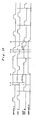
- the demodulation timing diagram shown in FIG. 10 shows waveforms, which are labeled, respectively, with Roman numbers that correspond to the identical numbers of points indicated in the circuit diagram of FIG. 8 where these waveforms are observed.
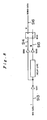
- a gate element U201 functions to drive the Delay Line. If the modulated signal S13 has a sufficient driving capacity, then this element may be omitted, and the circuit may be still functionable at an equivalent performance although it may be necessary to adjust the logic level.
- Gate elements U202 and U203 function to reform the waveform of the signal. If the waveform has a sufficient clarity as digital waveform, then these elements may be also omitted, and the circuit may be still functionable at an equivalent performance although it may be necessary to adjust the logic level.
- the Delay Line comprises passive elements and functions to delay the output, i.e., the passage of the signal being input, by the predetermined delay time Ty.
- the Delay Line which comprises passive elements, does not require a lock time as a PLL does, so the Delay Line can respond in real time in synchronization with the input signal.
- the output S14 of gate element U202 is input into the D-input terminal of flip-flop U204 while the output S15 (i.e., the modulated signal S13 delayed by the delay time Ty) of gate element U203 is input into the clock-input terminal of thereof.
- the flip-flop outputs a data signal S16, which is a demodulation version of the original data signal as described above in reference to FIGS. 5 and 6.
- the digital signal modulation and demodulation method of the present invention provides a simple circuit arrangement for modulation and demodulation of digital signals.
- the modulation circuit comprises only flip-flop circuits and gate elements, it can be manufactured easily as an IC, and the circuit elements can be realized inexpensively in simple arrangements.
- the demodulation circuit can be realized inexpensively in a simple arrangement because the circuit is designed to delay the modulated signal by a predetermined time (one period of a clock signal in the above embodiment) and to use the delayed signal as a clock signal for the demodulation. As a result, modulation and demodulation devices can be miniaturized.
Landscapes
- Physics & Mathematics (AREA)
- Spectroscopy & Molecular Physics (AREA)
- Engineering & Computer Science (AREA)
- Computer Networks & Wireless Communication (AREA)
- Signal Processing (AREA)
- Dc Digital Transmission (AREA)
Claims (5)
- Ein digitales Signalmodulations- und Demodulationsverfahren zur Übertragung eines digitalen Signals (S1), dessen Datenlogik mit einem H- und einem L-Pegel ausgedrückt wird, wobei besagtes digitales Signal (S1) zur Übertragung in ein moduliertes Signal (S12, S13) umgewandelt wird und bei Empfang demoduliert wird; wobei das besagte modulierte Signal (S12, S13) Impulssignale umfasst, mit Einschaltverhältnissen von H : L = N : 1 und 1 : N oder H : L = 1 : N und N : 1 (mit N > 1) in Übereinstimmung mit besagtem H-Pegel und besagtem L-Pegel von besagtem digitalen Signal (S1), dadurch gekennzeichnet, dass das besagte modulierte Signal (S13) mit Hilfe eines D-Flipflops (U204) demoduliert wird, um das besagte digitale Signal (S16) zu extrahieren, und dass das besagte modulierte Signal (S13) in einen D-Eingang des besagten D-Flipflops (U204) eingeleitet wird, während das besagte modulierte Signal, durch eine vorgegebene Verzögerungszeit Ty verzögert, in einen Takteingang hiervon eingeleitet wird zur Erzeugung eines demodulierten Datensignals an einem Q-Ausgang desselben.
- Das digitale Signalmodulations- und Demodulationsverfahren nach Anspruch 1, wobei die besagte vorgegebene Verzögerungszeit Ty so gewählt wird, dass ein bedingter Ausdruck: {1/(N+1)}Tm < Ty < {N/(N+1)}Tm erfüllt wird, wobei Tm die Dauer des modulierten Signals ist.
- Das digitale Signalmodulations- und Demodulationsverfahren nach Anspruch 1 oder 2, wobei das besagte modulierte Signal (S12, S13) Impulssignale umfasst mit Einschaltverhältnissen von H : L = 3 : 1 und 1 : 3 oder H : L = 1 : 3 und 3 : 1 in Übereinstimmung mit besagtem H-Pegel und besagtem L-Pegel des besagten digitalen Signals (S1).
- Das digitale Signalmodulations- und Demodulationsverfahren nach Anspruch 3, wobei die Dauer Tm des besagten modulierten Signals (S12, S13) bestimmt wird von zwei Zeitwerten 2T eines modulierten Taktsignals (S2) mit einer Dauer T, mit einem Verhältnis von Tm = 2T.
- Das digitale Signalmodulations- und Demodulationsverfahren nach Anspruch 4, wobei die besagte vorgegebene Verzögerungszeit Ty so gewählt wird, dass ein bedingter Ausdruck: (1/4)Tm < Ty < (3/4)Tm erfüllt wird.
Applications Claiming Priority (2)
| Application Number | Priority Date | Filing Date | Title |
|---|---|---|---|
| JP2002134396 | 2002-05-09 | ||
| JP2002134396 | 2002-05-09 |
Publications (2)
| Publication Number | Publication Date |
|---|---|
| EP1361718A1 EP1361718A1 (de) | 2003-11-12 |
| EP1361718B1 true EP1361718B1 (de) | 2005-06-01 |
Family
ID=29244181
Family Applications (1)
| Application Number | Title | Priority Date | Filing Date |
|---|---|---|---|
| EP03076282A Expired - Lifetime EP1361718B1 (de) | 2002-05-09 | 2003-04-10 | Pulsübertragungsmodulations- und -demodulationsverfahren |
Country Status (3)
| Country | Link |
|---|---|
| US (1) | US20030210748A1 (de) |
| EP (1) | EP1361718B1 (de) |
| DE (1) | DE60300748T2 (de) |
Families Citing this family (1)
| Publication number | Priority date | Publication date | Assignee | Title |
|---|---|---|---|---|
| CN113079071B (zh) * | 2020-01-06 | 2023-11-21 | 江苏固德威电源科技股份有限公司 | 一种单向走线实时检测数字信号的方法 |
Family Cites Families (14)
| Publication number | Priority date | Publication date | Assignee | Title |
|---|---|---|---|---|
| US3902129A (en) * | 1972-09-07 | 1975-08-26 | Ibm | Demodulating circuitry for pulse rate modulation data reproduction |
| JPS5634256A (en) * | 1979-08-29 | 1981-04-06 | Fuji Electric Co Ltd | Data transmission system |
| US4592072B1 (en) * | 1982-05-07 | 1994-02-15 | Digital Equipment Corporation | Decoder for self-clocking serial data communications |
| US4503472A (en) * | 1983-09-01 | 1985-03-05 | Burroughs Corp. | Bipolar time modulated encoder/decoder system |
| US4774446A (en) * | 1984-10-04 | 1988-09-27 | Pitney Bowes Inc. | Microprocessor controlled d.c. motor for controlling printing means |
| US4713841A (en) * | 1985-06-03 | 1987-12-15 | Itt Electro Optical Products, A Division Of Itt Corporation | Synchronous, asynchronous, data rate transparent fiber optic communications link |
| US5245635A (en) * | 1991-12-04 | 1993-09-14 | Honeywell Inc. | Clock recovery circuit for Manchester encoded data |
| US5481230A (en) * | 1994-11-14 | 1996-01-02 | Tektronix, Inc. | Phase modulator having individually placed edges |
| JP3378694B2 (ja) * | 1995-04-21 | 2003-02-17 | アルプス電気株式会社 | 情報伝送装置 |
| JP3080907B2 (ja) * | 1997-07-22 | 2000-08-28 | 日本電気アイシーマイコンシステム株式会社 | 変復調方法および変復調装置 |
| US5942977A (en) * | 1997-08-13 | 1999-08-24 | Ludwig Kipp | Radio transponder |
| US5838210A (en) * | 1997-12-01 | 1998-11-17 | Motorola, Inc. | Method and apparatus for generating a modulated signal |
| US7369609B2 (en) * | 2003-04-01 | 2008-05-06 | The Boeing Company | Duty factor encoded data and clock transmission |
| US6947493B2 (en) * | 2003-10-10 | 2005-09-20 | Atmel Corporation | Dual phase pulse modulation decoder circuit |
-
2003
- 2003-04-10 EP EP03076282A patent/EP1361718B1/de not_active Expired - Lifetime
- 2003-04-10 DE DE60300748T patent/DE60300748T2/de not_active Expired - Fee Related
- 2003-05-01 US US10/427,289 patent/US20030210748A1/en not_active Abandoned
Also Published As
| Publication number | Publication date |
|---|---|
| EP1361718A1 (de) | 2003-11-12 |
| US20030210748A1 (en) | 2003-11-13 |
| DE60300748T2 (de) | 2006-05-11 |
| DE60300748D1 (de) | 2005-07-07 |
Similar Documents
| Publication | Publication Date | Title |
|---|---|---|
| CA1198780A (en) | Self-clocking binary receiver | |
| US5446770A (en) | Time division duplex transceiver | |
| US5365548A (en) | Digital FSK transmitter | |
| CN113949374A (zh) | 具有脉冲载波调制的数字隔离器电路 | |
| US8437377B2 (en) | Pulse generator, transmitter-receiver, and pulse generation method | |
| EP1361718A1 (de) | Pulsübertragungsmodulations- und -demodulationsverfahren | |
| US20060133558A1 (en) | Mechanism to aid a phase interpolator in recovering a clock signal | |
| WO2006051735A1 (ja) | 変調回路、および、それを用いた送信装置、受信装置、および通信システム | |
| US4503472A (en) | Bipolar time modulated encoder/decoder system | |
| US2708268A (en) | Sequential phase-shifted amplitude modulated carrier wave | |
| JP2004032677A (ja) | デジタル信号の変調・復調方式 | |
| RU2115172C1 (ru) | Способ передачи информации и устройство для его осуществления | |
| SU363198A1 (ru) | УСТРОЙСТВО дл ПРЕОБРАЗОВАНИЯ ЧАСТОТНО-МОДУЛИРОВАННОГО СИГНАЛА | |
| SU1451872A1 (ru) | Устройство дл передачи и приема дискретных сигналов | |
| SU1290557A1 (ru) | Система дл передачи и приема дискретной информации | |
| JPH04158640A (ja) | デジタル通信方式 | |
| JP3277038B2 (ja) | 光伝送装置 | |
| SU1223385A1 (ru) | Система св зи с многоосновным кодированием | |
| SU1559417A1 (ru) | Устройство дл приема дискретных сообщений | |
| KR100526937B1 (ko) | 디퍼런셜코드발생기 | |
| SU1256233A1 (ru) | Система дл передачи цифровой информации по проводным каналам св зи | |
| RU2022481C1 (ru) | Система передачи и приема первичного и вторичного потоков данных | |
| US20020163984A1 (en) | Clock and data recovery unit based on class B amplifier | |
| JPH01143435A (ja) | データ伝送装置 | |
| SU1069175A1 (ru) | Система св зи с многоосновным кодированием |
Legal Events
| Date | Code | Title | Description |
|---|---|---|---|
| PUAI | Public reference made under article 153(3) epc to a published international application that has entered the european phase |
Free format text: ORIGINAL CODE: 0009012 |
|
| AK | Designated contracting states |
Kind code of ref document: A1 Designated state(s): AT BE BG CH CY CZ DE DK EE ES FI FR GB GR HU IE IT LI LU MC NL PT RO SE SI SK TR |
|
| AX | Request for extension of the european patent |
Extension state: AL LT LV MK |
|
| 17P | Request for examination filed |
Effective date: 20040512 |
|
| 17Q | First examination report despatched |
Effective date: 20040603 |
|
| AKX | Designation fees paid |
Designated state(s): DE NL |
|
| GRAP | Despatch of communication of intention to grant a patent |
Free format text: ORIGINAL CODE: EPIDOSNIGR1 |
|
| GRAS | Grant fee paid |
Free format text: ORIGINAL CODE: EPIDOSNIGR3 |
|
| GRAA | (expected) grant |
Free format text: ORIGINAL CODE: 0009210 |
|
| AK | Designated contracting states |
Kind code of ref document: B1 Designated state(s): DE NL |
|
| REF | Corresponds to: |
Ref document number: 60300748 Country of ref document: DE Date of ref document: 20050707 Kind code of ref document: P |
|
| PLBE | No opposition filed within time limit |
Free format text: ORIGINAL CODE: 0009261 |
|
| STAA | Information on the status of an ep patent application or granted ep patent |
Free format text: STATUS: NO OPPOSITION FILED WITHIN TIME LIMIT |
|
| 26N | No opposition filed |
Effective date: 20060302 |
|
| PG25 | Lapsed in a contracting state [announced via postgrant information from national office to epo] |
Ref country code: DE Free format text: LAPSE BECAUSE OF NON-PAYMENT OF DUE FEES Effective date: 20061101 |
|
| NLV4 | Nl: lapsed or anulled due to non-payment of the annual fee |
Effective date: 20071101 |
|
| PG25 | Lapsed in a contracting state [announced via postgrant information from national office to epo] |
Ref country code: NL Free format text: LAPSE BECAUSE OF NON-PAYMENT OF DUE FEES Effective date: 20071101 |