EP1356136B1 - Method for producing electrical conductors and use thereof for solar collector and electrochemical cell - Google Patents
Method for producing electrical conductors and use thereof for solar collector and electrochemical cell Download PDFInfo
- Publication number
- EP1356136B1 EP1356136B1 EP02710565A EP02710565A EP1356136B1 EP 1356136 B1 EP1356136 B1 EP 1356136B1 EP 02710565 A EP02710565 A EP 02710565A EP 02710565 A EP02710565 A EP 02710565A EP 1356136 B1 EP1356136 B1 EP 1356136B1
- Authority
- EP
- European Patent Office
- Prior art keywords
- skeleton
- screen material
- openings
- copper
- range
- Prior art date
- Legal status (The legal status is an assumption and is not a legal conclusion. Google has not performed a legal analysis and makes no representation as to the accuracy of the status listed.)
- Expired - Lifetime
Links
- 239000004020 conductor Substances 0.000 title claims abstract description 27
- 238000004519 manufacturing process Methods 0.000 title claims abstract description 7
- 239000000463 material Substances 0.000 claims abstract description 43
- RYGMFSIKBFXOCR-UHFFFAOYSA-N Copper Chemical compound [Cu] RYGMFSIKBFXOCR-UHFFFAOYSA-N 0.000 claims abstract description 26
- 238000000034 method Methods 0.000 claims abstract description 23
- 239000010949 copper Substances 0.000 claims abstract description 21
- 229910052802 copper Inorganic materials 0.000 claims abstract description 19
- 238000004070 electrodeposition Methods 0.000 claims abstract description 17
- 239000011159 matrix material Substances 0.000 claims abstract description 16
- 238000005323 electroforming Methods 0.000 claims abstract description 13
- 239000011133 lead Substances 0.000 claims description 10
- 239000002184 metal Substances 0.000 claims description 9
- 229910052751 metal Inorganic materials 0.000 claims description 9
- 238000000151 deposition Methods 0.000 claims description 4
- 230000008021 deposition Effects 0.000 claims description 3
- 229910052745 lead Inorganic materials 0.000 claims description 3
- 229910052759 nickel Inorganic materials 0.000 claims description 3
- 239000002344 surface layer Substances 0.000 claims description 3
- 229910045601 alloy Inorganic materials 0.000 claims description 2
- 239000000956 alloy Substances 0.000 claims description 2
- 229910052793 cadmium Inorganic materials 0.000 claims description 2
- 238000006243 chemical reaction Methods 0.000 claims description 2
- 229910052709 silver Inorganic materials 0.000 claims description 2
- 229910052725 zinc Inorganic materials 0.000 claims description 2
- 238000003860 storage Methods 0.000 abstract description 3
- 238000005868 electrolysis reaction Methods 0.000 abstract description 2
- 239000000126 substance Substances 0.000 description 5
- 239000000758 substrate Substances 0.000 description 5
- 230000000694 effects Effects 0.000 description 4
- 239000007772 electrode material Substances 0.000 description 4
- 239000007788 liquid Substances 0.000 description 4
- 238000007788 roughening Methods 0.000 description 4
- PXHVJJICTQNCMI-UHFFFAOYSA-N Nickel Chemical compound [Ni] PXHVJJICTQNCMI-UHFFFAOYSA-N 0.000 description 3
- 239000011888 foil Substances 0.000 description 3
- 150000002739 metals Chemical class 0.000 description 3
- XEEYBQQBJWHFJM-UHFFFAOYSA-N Iron Chemical compound [Fe] XEEYBQQBJWHFJM-UHFFFAOYSA-N 0.000 description 2
- AFVFQIVMOAPDHO-UHFFFAOYSA-N Methanesulfonic acid Chemical compound CS(O)(=O)=O AFVFQIVMOAPDHO-UHFFFAOYSA-N 0.000 description 2
- 239000003792 electrolyte Substances 0.000 description 2
- 238000005530 etching Methods 0.000 description 2
- -1 for example Substances 0.000 description 2
- 239000011148 porous material Substances 0.000 description 2
- 238000007639 printing Methods 0.000 description 2
- 238000004080 punching Methods 0.000 description 2
- 238000007650 screen-printing Methods 0.000 description 2
- 239000011343 solid material Substances 0.000 description 2
- 230000008719 thickening Effects 0.000 description 2
- HBBGRARXTFLTSG-UHFFFAOYSA-N Lithium ion Chemical compound [Li+] HBBGRARXTFLTSG-UHFFFAOYSA-N 0.000 description 1
- 208000012868 Overgrowth Diseases 0.000 description 1
- 230000002378 acidificating effect Effects 0.000 description 1
- 239000000654 additive Substances 0.000 description 1
- 238000005282 brightening Methods 0.000 description 1
- OJIJEKBXJYRIBZ-UHFFFAOYSA-N cadmium nickel Chemical compound [Ni].[Cd] OJIJEKBXJYRIBZ-UHFFFAOYSA-N 0.000 description 1
- 239000003795 chemical substances by application Substances 0.000 description 1
- 150000001879 copper Chemical class 0.000 description 1
- 239000011889 copper foil Substances 0.000 description 1
- ARUVKPQLZAKDPS-UHFFFAOYSA-L copper(II) sulfate Chemical compound [Cu+2].[O-][S+2]([O-])([O-])[O-] ARUVKPQLZAKDPS-UHFFFAOYSA-L 0.000 description 1
- JZCCFEFSEZPSOG-UHFFFAOYSA-L copper(II) sulfate pentahydrate Chemical compound O.O.O.O.O.[Cu+2].[O-]S([O-])(=O)=O JZCCFEFSEZPSOG-UHFFFAOYSA-L 0.000 description 1
- DOBRDRYODQBAMW-UHFFFAOYSA-N copper(i) cyanide Chemical compound [Cu+].N#[C-] DOBRDRYODQBAMW-UHFFFAOYSA-N 0.000 description 1
- 230000001419 dependent effect Effects 0.000 description 1
- PEVJCYPAFCUXEZ-UHFFFAOYSA-J dicopper;phosphonato phosphate Chemical compound [Cu+2].[Cu+2].[O-]P([O-])(=O)OP([O-])([O-])=O PEVJCYPAFCUXEZ-UHFFFAOYSA-J 0.000 description 1
- 239000011810 insulating material Substances 0.000 description 1
- 229910052742 iron Inorganic materials 0.000 description 1
- 229910001416 lithium ion Inorganic materials 0.000 description 1
- 238000003754 machining Methods 0.000 description 1
- 229910052987 metal hydride Inorganic materials 0.000 description 1
- 238000001465 metallisation Methods 0.000 description 1
- 239000000203 mixture Substances 0.000 description 1
- QELJHCBNGDEXLD-UHFFFAOYSA-N nickel zinc Chemical compound [Ni].[Zn] QELJHCBNGDEXLD-UHFFFAOYSA-N 0.000 description 1
- 229920002120 photoresistant polymer Polymers 0.000 description 1
- 229920000642 polymer Polymers 0.000 description 1
- 238000007873 sieving Methods 0.000 description 1
- 239000007787 solid Substances 0.000 description 1
- 239000007858 starting material Substances 0.000 description 1
- 239000011701 zinc Substances 0.000 description 1
Images

Classifications
-
- C—CHEMISTRY; METALLURGY
- C25—ELECTROLYTIC OR ELECTROPHORETIC PROCESSES; APPARATUS THEREFOR
- C25D—PROCESSES FOR THE ELECTROLYTIC OR ELECTROPHORETIC PRODUCTION OF COATINGS; ELECTROFORMING; APPARATUS THEREFOR
- C25D1/00—Electroforming
- C25D1/08—Perforated or foraminous objects, e.g. sieves
-
- C—CHEMISTRY; METALLURGY
- C25—ELECTROLYTIC OR ELECTROPHORETIC PROCESSES; APPARATUS THEREFOR
- C25D—PROCESSES FOR THE ELECTROLYTIC OR ELECTROPHORETIC PRODUCTION OF COATINGS; ELECTROFORMING; APPARATUS THEREFOR
- C25D1/00—Electroforming
- C25D1/04—Wires; Strips; Foils
-
- C—CHEMISTRY; METALLURGY
- C25—ELECTROLYTIC OR ELECTROPHORETIC PROCESSES; APPARATUS THEREFOR
- C25D—PROCESSES FOR THE ELECTROLYTIC OR ELECTROPHORETIC PRODUCTION OF COATINGS; ELECTROFORMING; APPARATUS THEREFOR
- C25D1/00—Electroforming
- C25D1/10—Moulds; Masks; Masterforms
-
- C—CHEMISTRY; METALLURGY
- C25—ELECTROLYTIC OR ELECTROPHORETIC PROCESSES; APPARATUS THEREFOR
- C25D—PROCESSES FOR THE ELECTROLYTIC OR ELECTROPHORETIC PRODUCTION OF COATINGS; ELECTROFORMING; APPARATUS THEREFOR
- C25D3/00—Electroplating: Baths therefor
- C25D3/02—Electroplating: Baths therefor from solutions
- C25D3/48—Electroplating: Baths therefor from solutions of gold
-
- H—ELECTRICITY
- H01—ELECTRIC ELEMENTS
- H01M—PROCESSES OR MEANS, e.g. BATTERIES, FOR THE DIRECT CONVERSION OF CHEMICAL ENERGY INTO ELECTRICAL ENERGY
- H01M4/00—Electrodes
- H01M4/02—Electrodes composed of, or comprising, active material
- H01M4/64—Carriers or collectors
- H01M4/70—Carriers or collectors characterised by shape or form
- H01M4/72—Grids
- H01M4/74—Meshes or woven material; Expanded metal
-
- Y—GENERAL TAGGING OF NEW TECHNOLOGICAL DEVELOPMENTS; GENERAL TAGGING OF CROSS-SECTIONAL TECHNOLOGIES SPANNING OVER SEVERAL SECTIONS OF THE IPC; TECHNICAL SUBJECTS COVERED BY FORMER USPC CROSS-REFERENCE ART COLLECTIONS [XRACs] AND DIGESTS
- Y02—TECHNOLOGIES OR APPLICATIONS FOR MITIGATION OR ADAPTATION AGAINST CLIMATE CHANGE
- Y02E—REDUCTION OF GREENHOUSE GAS [GHG] EMISSIONS, RELATED TO ENERGY GENERATION, TRANSMISSION OR DISTRIBUTION
- Y02E60/00—Enabling technologies; Technologies with a potential or indirect contribution to GHG emissions mitigation
- Y02E60/10—Energy storage using batteries
Definitions
- the invention relates to a method for producing an electrical conductor suitable for use in a device for conversion of energy.
- Copper screen material which if desired may be nickel-plated, for use as current conductors in batteries and storage batteries is known per se in the art.
- US Patent 4,328,293 discloses a positive electrode for an electrochemical cell (generator), which electrode comprises a conductive substrate which comprises, for example, a perforated and nickel-plated copper strip.
- US-A-4,228,224 discloses a copper screen material of 80 mesh which is used in a positive electrode.
- a porous metal, for example, copper, foil is known for use as electrode material, which is obtained by the electroforming of a mechanically roughened substrate to form a metal foil with a thickness ranging from a few tens to a few hundreds of micrometers.
- the foil formed in this way is peeled off the substrate, or the substrate is dissolved.
- the reproducibility of machining of the substrate is low, so that products with different characteristics of the pores, such as the dimensions thereof, and therefore also of the overall conductivity, are in each case obtained.
- it is unclear how the pores are obtained in accordance with this Japanese Patent Application.
- the present invention is based on the general object of avoiding the above drawbacks.
- it is an object of the invention to provide electrical conductors having a large volume, contact surface area and good adhesion for active chemical material.
- it is an object of the invention to provide an alternative way of roughening the conductor.
- a method for the production of an electrical conductor which conductor comprises a copper-containing screen material, is characterized in that the method comprises the steps of:
- the method according to the invention comprises after step c), or after step b) when step c) is not applied, a step d) of further growth of the skeleton by electrodeposition of lead to form screen material.
- a step d) of further growth of the skeleton by electrodeposition of lead to form screen material For example, by introducing the screen material in an electrodeposition bath containing leadmethanesulphonate and methanesulphonic acid.
- a skeleton of screen material is deposited on an electroforming matrix which is connected as cathode, from a suitable electrodeposition bath for the deposition of copper.
- An electroforming matrix of this type which may, for example, be flat or cylindrical, comprises a surface which includes conductive parts, generally in the form of a regular network of interconnected metal dykes, which dykes are delimited by nonconductive parts made from an insulating material, for example photoresist.
- a skeleton of copper screen material is formed, the screen openings being delimited by copper dykes corresponding to the pattern of the electroforming matrix.
- some lateral overgrowth over the nonconductive parts of the electroforming matrix may occur.
- the open surface area of the screen material obtained will be preferably at least equal to a minimum open surface area, which is determined experimentally in order to obtain the desired advantageous characteristics of the conductor. The lower the density of holes, the higher the minimum open surface area.
- a method of forming a sieve material by thickening a previously formed, electrically conducting sieve skeleton by metal deposition in an electrolysis bath is known per se from EP-A1-0 492 731.
- nickel and iron are mentioned in the preferred embodiments, while in principle all electrolytically depositable metals can be used in the thickening step.
- the sieve material thus produced is suitable for various purposes such as screen printing and sieving.
- copper is mentioned as one of the electrolytically depositable metals it is not used in printing screens, because copper will dissolve in the printing ink and pastes conveniently used in screen printing.
- the copper bath used may be a conventional electrodeposition bath, such as acidic Cu baths, or baths with an electrolyte such as copper sulphate, copper cyanide, copper fluoroborate, copper pyrophosphate and the like.
- An example of a bath of this type comprises: CuSO 4 .5H 2 O 150-250 g/l H 8 SO 4 50-100 g/l Cl - 0-50 mg/l.
- the current density is in the range 1-70 A/dm 2 , preferably 10-50 A/dm 2 .
- the thickness of the skeleton, and therefore of the screen material is preferably in the range of 10-45 micrometers. This level of thickness offers sufficient strength to remove the skeleton from the matrix.
- the dimensions and shape of the openings may vary.
- the diameter preferably lies in the range of 50-100 micrometers. This preferred range is determined by factors such as open surface area, mesh number and technical feasibility.
- the skeleton is grown further by conventional deposition techniques by deposition of a metal which is preferably selected from the group comprising Ag, Zn, Cd, Ni, Pb and Cu or alloys, Cu and Pb being the more preferred metals of this group.
- the skeleton is advantageously further grown with Cu in an electrodeposition bath, the skeleton being (electrically) connected as cathode.
- a further growth of the skeleton with Pb may be accomplished by introducing the screen material in an electrodeposition bath containing leadmethanesulphonate and methanesulphonic acid.
- the final thickness of the screen material is then advantageously over 15 micrometers, preferably in the range of 20-70 micrometers, so that the screen material is still easy to deform, for example to wind.
- this deformation it can be stated in general terms that the thinner the material, the easier the deformation.
- the further growth accomplished by step d) complies with the condition 0.5 ⁇ (a+b)/(c+d) ⁇ 5, wherein a+b denotes the further growth in the thickness direction of the skeleton and c+d denotes the further growth in the plane of the skeleton.
- Screen material which complies with this condition allows of the application of electrically conductive paste in the screen openings from one side. If the values are higher, i.e. a relatively thick further growth, the application of paste, even from two sides, becomes more difficult, with a high probability of air bubbles being included in the paste. This is undesirable with regard to conductivity.
- This further growth can be controlled by adding additives (brightening agents) to the composition of the electrodeposition bath, by applying a forced flow of liquid, which for example passes through the openings in the skeleton, and by adjusting the current density.
- additives for example passes through the openings in the skeleton
- current density for example passes through the openings in the skeleton
- An electrical conductor which is produced using the method according to the invention does not have any sharp edges and is therefore easy to handle as an electrode compared to punched or stamped electrode materials.
- an electrical conductor produced in accordance with the invention is characterised by a more uniform thickness, hole shape and hole size.
- the method according to the invention also allows the production of electrodes with finer grids of openings.
- the screen material When used as an electrode, the screen material provides more space for active chemical material, and the contact surface between screen material and active chemical material is greater.
- a copper foil with a thickness of 35 micrometers and a grid of hexagonal openings of 155 mesh and an open surface area of approx. 10% (approx. 3800 openings/cm 2 ) has an additional contact surface area of approximately 15% compared to solid material.
- this contact surface area is further enhanced by the roughening effect of the method according to the invention on the resultant surface of the conductor.
- This roughening effect is particularly strong when lead is deposited as a surface layer. In general, the roughening effect is dependent on the working conditions of the method according to the invention.
- the invention also relates to a solar collector comprising a current collector, made of an electroformed screen material comprising a copper skeleton wherein the screen material has a density of openings that lies in the range of 1-20,000 openings/cm 2 .
- the invention furthermore relates to an electrochemical cell comprising an electrode made of an electroformed screen material comprising a copper skeleton wherein the screen material has a density of openings that lies in the range of 1-20,000 openings/cm 2 .
- the electrical conductors produced using the method according to the invention can be used as electrically conductive electrode material in batteries and storage batteries, including types based on lithium-ion, lithium-polymer, nickel-cadmium, nickel-metal hydride, zinc-air, nickel-zinc and lead. Another possible application is as a current collector in solar collectors.
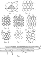
- this figure shows a skeleton dyke 10 in cross section. For the sake of clarity, only this skeleton web is depicted in hatched form.
- This skeleton has been produced in the manner described above in accordance with the first aspect of the invention.
- the planar underside of the skeleton dyke 10 is the side which has been grown onto the metal conductors of the electroforming matrix and includes, as it were, an impression of the shape of the conductor. After the skeleton formed has been removed from the matrix applied, this skeleton is grown further in an electrodeposition bath while a forced flow of liquid is maintained through the openings of the skeleton, to form a screen material with copper dykes 12.
- the further growth in the direction of the flow of liquid i.e. the thickness direction of the skeleton, denoted by a and b, is greater than the further growth in a direction perpendicular to the flow of liquid, in this figure indicated by c and d.
- Fig. 2-9 show examples of patterns of interconnected conductive dykes 14 which are separated by nonconductive islands 16, as may be provided in a matrix which is used in a method according to the first aspect.
- the nonconductive islands 16, which correspond to the openings which are to be formed may adopt various shapes and dimensions, even within a pattern.
- Fig. 9 shows a grid with slot shaped openings 16 between dykes 14, wherein the arrow 32 indicates the orientation of high conductance of the conductor and arrow 30 of low conductance of the conductor, respectively.
- Such a discrimination in conductance by the pattern of the conductor is of interest when the conductor is used in powertools and EV's, for instance.
- the table I below shows the maximum open surface area as a function of the number of holes/cm 2 for screen materials with a total thickness of 20 micrometers which have been produced on an electroforming matrix with a minimum dyke width of 15 micrometers and a hexagonal grid, as shown in Fig. 2.
- Holes/cm 2 Mesh No. Dyke Width Matrix ( ⁇ m) Skeleton Thickness ( ⁇ m) Skeleton Open Surface Area (%) Min. Max. 1 2.4 100 20 40 97 10 7.5 100 20 30 92 100 24 70 20 20 80 1000 75 30 20 10 63 10000 235 15 20 5 24 10000 235 15 10 5 45 20000 335 15 20 3 7.5 20000 335 15 10 3 30
- Fig. 10 shows a graph representing this information.
- a conductor according to the invention has a minimum value for the open surface area (MIN. OPEN SURFACE AREA) in combination with a specific thickness and mesh number, since otherwise the advantages compared to solid material are only marginal. The maximum value is determined by the technique employed. As can be seen, the open surface area can be increased, which offers advantages in particular for the higher mesh numbers (generally a density of holes which is greater than or equal to 10,000), by producing the screen material in two steps. Obviously, even when using the two-step method, a conductor obtained has to comply with the condition relating to the minimum open surface area.
- the maximum open surface area is delimited by practical limitations.
Landscapes
- Chemical & Material Sciences (AREA)
- Chemical Kinetics & Catalysis (AREA)
- Electrochemistry (AREA)
- Engineering & Computer Science (AREA)
- Materials Engineering (AREA)
- Metallurgy (AREA)
- Organic Chemistry (AREA)
- General Chemical & Material Sciences (AREA)
- Cell Electrode Carriers And Collectors (AREA)
- Electroplating Methods And Accessories (AREA)
- Hybrid Cells (AREA)
- Photovoltaic Devices (AREA)
Applications Claiming Priority (3)
| Application Number | Priority Date | Filing Date | Title |
|---|---|---|---|
| NL1017213A NL1017213C2 (nl) | 2001-01-29 | 2001-01-29 | Werkwijzen voor het vervaardigen van elektrische geleiders, en toepassing van aldus vervaardigde geleiders. |
| NL1017213 | 2001-01-29 | ||
| PCT/NL2002/000064 WO2002061184A1 (en) | 2001-01-29 | 2002-01-28 | Method for producing electrical conductors, a solar collector, an electrochemical cell and use of conductors produced in this way |
Publications (2)
| Publication Number | Publication Date |
|---|---|
| EP1356136A1 EP1356136A1 (en) | 2003-10-29 |
| EP1356136B1 true EP1356136B1 (en) | 2004-11-24 |
Family
ID=19772808
Family Applications (1)
| Application Number | Title | Priority Date | Filing Date |
|---|---|---|---|
| EP02710565A Expired - Lifetime EP1356136B1 (en) | 2001-01-29 | 2002-01-28 | Method for producing electrical conductors and use thereof for solar collector and electrochemical cell |
Country Status (9)
| Country | Link |
|---|---|
| US (1) | US20040115536A1 (enExample) |
| EP (1) | EP1356136B1 (enExample) |
| JP (1) | JP2004522856A (enExample) |
| KR (1) | KR20040035590A (enExample) |
| AT (1) | ATE283384T1 (enExample) |
| CA (1) | CA2436244A1 (enExample) |
| DE (1) | DE60202048T2 (enExample) |
| NL (1) | NL1017213C2 (enExample) |
| WO (1) | WO2002061184A1 (enExample) |
Families Citing this family (14)
| Publication number | Priority date | Publication date | Assignee | Title |
|---|---|---|---|---|
| CN101305432B (zh) * | 2005-11-14 | 2012-02-22 | 松下电器产业株式会社 | 双电层电容器 |
| US8321859B2 (en) * | 2005-12-22 | 2012-11-27 | Alan Joshua Shapiro | Method and apparatus for dispensing on a data-storage medium customized content comprising selected assets |
| EP2508652B1 (en) * | 2009-12-04 | 2017-03-22 | Mitsui Mining & Smelting Co., Ltd | Porous metal foil and method for manufacturing the same |
| JP2011216364A (ja) * | 2010-03-31 | 2011-10-27 | Toyo Aluminium Kk | 負極集電体用金属箔 |
| JP5636291B2 (ja) * | 2011-01-13 | 2014-12-03 | 三井金属鉱業株式会社 | 補強された多孔質金属箔およびその製造方法 |
| JP5400826B2 (ja) * | 2011-04-08 | 2014-01-29 | 三井金属鉱業株式会社 | 複合金属箔およびその製造方法 |
| US8936709B2 (en) * | 2013-03-13 | 2015-01-20 | Gtat Corporation | Adaptable free-standing metallic article for semiconductors |
| US20150129024A1 (en) * | 2013-11-13 | 2015-05-14 | Gtat Corporation | Free-Standing Metallic Article With Expansion Segment |
| US20140261661A1 (en) * | 2013-03-13 | 2014-09-18 | Gtat Corporation | Free-standing metallic article with overplating |
| US8916038B2 (en) * | 2013-03-13 | 2014-12-23 | Gtat Corporation | Free-standing metallic article for semiconductors |
| TWI612685B (zh) * | 2013-03-13 | 2018-01-21 | 梅林太陽能科技股份有限公司 | 用於半導體之可適應自站立金屬物件 |
| US8569096B1 (en) * | 2013-03-13 | 2013-10-29 | Gtat Corporation | Free-standing metallic article for semiconductors |
| WO2015138188A1 (en) * | 2014-03-12 | 2015-09-17 | Gtat Corporation | Photovoltaic module with flexible circuit |
| US9573214B2 (en) * | 2014-08-08 | 2017-02-21 | Merlin Solar Technologies, Inc. | Solder application method and apparatus |
Family Cites Families (4)
| Publication number | Priority date | Publication date | Assignee | Title |
|---|---|---|---|---|
| DE2819339A1 (de) * | 1978-05-03 | 1979-11-08 | Veco Beheer Electro Photo | Verfahren zur herstellung eines siebes, insbesondere eines feinen siebes, mit einem stuetzkoerper |
| US4228224A (en) * | 1979-04-12 | 1980-10-14 | Rockwell International Corporation | Positive electrode for electrical energy storage device |
| FR2468212A1 (fr) * | 1979-10-16 | 1981-04-30 | Citroen Sa | Perfectionnements apportes aux generateurs electrochimiques |
| NL9002866A (nl) * | 1990-12-24 | 1992-07-16 | Stork Screens Bv | Werkwijze voor het vormen van een zeefmateriaal met lage inwendige spanning en aldus verkregen zeefmateriaal. |
-
2001
- 2001-01-29 NL NL1017213A patent/NL1017213C2/nl not_active IP Right Cessation
-
2002
- 2002-01-28 JP JP2002561113A patent/JP2004522856A/ja active Pending
- 2002-01-28 EP EP02710565A patent/EP1356136B1/en not_active Expired - Lifetime
- 2002-01-28 WO PCT/NL2002/000064 patent/WO2002061184A1/en not_active Ceased
- 2002-01-28 KR KR10-2003-7010008A patent/KR20040035590A/ko not_active Ceased
- 2002-01-28 AT AT02710565T patent/ATE283384T1/de not_active IP Right Cessation
- 2002-01-28 US US10/470,184 patent/US20040115536A1/en not_active Abandoned
- 2002-01-28 CA CA002436244A patent/CA2436244A1/en not_active Abandoned
- 2002-01-28 DE DE60202048T patent/DE60202048T2/de not_active Expired - Fee Related
Also Published As
| Publication number | Publication date |
|---|---|
| CA2436244A1 (en) | 2002-08-08 |
| JP2004522856A (ja) | 2004-07-29 |
| US20040115536A1 (en) | 2004-06-17 |
| EP1356136A1 (en) | 2003-10-29 |
| WO2002061184A1 (en) | 2002-08-08 |
| KR20040035590A (ko) | 2004-04-29 |
| ATE283384T1 (de) | 2004-12-15 |
| DE60202048T2 (de) | 2005-03-31 |
| DE60202048D1 (de) | 2004-12-30 |
| NL1017213C2 (nl) | 2002-07-30 |
Similar Documents
| Publication | Publication Date | Title |
|---|---|---|
| EP1356136B1 (en) | Method for producing electrical conductors and use thereof for solar collector and electrochemical cell | |
| JP4037229B2 (ja) | リチウム二次電池用電極と、これを負極とするリチウム二次電池 | |
| CN112956049B (zh) | 金属锂负极及其制备方法、利用它的锂二次电池 | |
| US9493885B2 (en) | Lithium-ion batteries with nanostructured electrodes and associated methods of making | |
| JP4616584B2 (ja) | 非水電解液二次電池用負極 | |
| EP2557617B1 (en) | Lithium secondary battery and anode therefor | |
| EP2432057A1 (en) | Lithium secondary battery and anode therefor | |
| KR20140024457A (ko) | 나노구조형 전극이 있는 배터리 및 관련 방법 | |
| JPH08236120A (ja) | 多孔質電解金属箔の製造方法、その電解金属箔を用いた二次電池用電極 | |
| EP0860518B1 (en) | Process for preparing porous electrolytic metal foil | |
| CN108122691B (zh) | 锂离子电容器集流体箔材及其制造方法 | |
| JP2004522856A5 (enExample) | ||
| KR20190108316A (ko) | 수소 거품 형판을 이용한 다공성 전극 집전체의 제조방법 및 상기 방법에 의해 제조된 전극 집전체 | |
| KR102085499B1 (ko) | 수소 거품 형판을 이용한 다공성 전극 집전체의 제조방법 및 상기 방법에 의해 제조된 전극 집전체 | |
| WO2021173469A1 (en) | Electrode having protective and locking layers on current collector | |
| JP2013008540A (ja) | 非水電解質二次電池用集電体及びそれを用いた電極 | |
| JP4298578B2 (ja) | キャリア箔付き多孔質金属箔及びその製造方法 | |
| JPH06314566A (ja) | 蓄電池用電極 | |
| JP3245837B2 (ja) | 多孔性金属箔の製造方法 | |
| JP2002216771A (ja) | 二次電池負極集電体用電解金属箔およびその製造方法 | |
| KR102879700B1 (ko) | 다공성 구조를 갖는 구리박의 제조방법 | |
| JP2002025573A (ja) | 燃料電池用電極の製造方法 | |
| KR102800663B1 (ko) | 적층된 전극을 포함하는 마그네슘 전지용 음극 및 그의 제조 방법 | |
| US3320139A (en) | Method for preparing negative electrodes | |
| JPS63128192A (ja) | 孔開き金属薄帯の製造方法 |
Legal Events
| Date | Code | Title | Description |
|---|---|---|---|
| PUAI | Public reference made under article 153(3) epc to a published international application that has entered the european phase |
Free format text: ORIGINAL CODE: 0009012 |
|
| 17P | Request for examination filed |
Effective date: 20030718 |
|
| AK | Designated contracting states |
Kind code of ref document: A1 Designated state(s): AT BE CH CY DE DK ES FI FR GB GR IE IT LI LU MC NL PT SE TR |
|
| AX | Request for extension of the european patent |
Extension state: AL LT LV MK RO SI |
|
| GRAP | Despatch of communication of intention to grant a patent |
Free format text: ORIGINAL CODE: EPIDOSNIGR1 |
|
| RTI1 | Title (correction) |
Free format text: METHOD FOR PRODUCING ELECTRICAL CONDUCTORS AND USE THEREOF FOR SOLAR COLLECTOR AND ELECTROCHEMICAL CELL |
|
| GRAS | Grant fee paid |
Free format text: ORIGINAL CODE: EPIDOSNIGR3 |
|
| GRAA | (expected) grant |
Free format text: ORIGINAL CODE: 0009210 |
|
| AK | Designated contracting states |
Kind code of ref document: B1 Designated state(s): AT BE CH CY DE DK ES FI FR GB GR IE IT LI LU MC NL PT SE TR |
|
| PG25 | Lapsed in a contracting state [announced via postgrant information from national office to epo] |
Ref country code: IT Free format text: LAPSE BECAUSE OF FAILURE TO SUBMIT A TRANSLATION OF THE DESCRIPTION OR TO PAY THE FEE WITHIN THE PRESCRIBED TIME-LIMIT;WARNING: LAPSES OF ITALIAN PATENTS WITH EFFECTIVE DATE BEFORE 2007 MAY HAVE OCCURRED AT ANY TIME BEFORE 2007. THE CORRECT EFFECTIVE DATE MAY BE DIFFERENT FROM THE ONE RECORDED. Effective date: 20041124 Ref country code: TR Free format text: LAPSE BECAUSE OF FAILURE TO SUBMIT A TRANSLATION OF THE DESCRIPTION OR TO PAY THE FEE WITHIN THE PRESCRIBED TIME-LIMIT Effective date: 20041124 Ref country code: FI Free format text: LAPSE BECAUSE OF FAILURE TO SUBMIT A TRANSLATION OF THE DESCRIPTION OR TO PAY THE FEE WITHIN THE PRESCRIBED TIME-LIMIT Effective date: 20041124 Ref country code: LI Free format text: LAPSE BECAUSE OF FAILURE TO SUBMIT A TRANSLATION OF THE DESCRIPTION OR TO PAY THE FEE WITHIN THE PRESCRIBED TIME-LIMIT Effective date: 20041124 Ref country code: CH Free format text: LAPSE BECAUSE OF FAILURE TO SUBMIT A TRANSLATION OF THE DESCRIPTION OR TO PAY THE FEE WITHIN THE PRESCRIBED TIME-LIMIT Effective date: 20041124 |
|
| REG | Reference to a national code |
Ref country code: GB Ref legal event code: FG4D |
|
| REG | Reference to a national code |
Ref country code: CH Ref legal event code: EP |
|
| REF | Corresponds to: |
Ref document number: 60202048 Country of ref document: DE Date of ref document: 20041230 Kind code of ref document: P |
|
| REG | Reference to a national code |
Ref country code: IE Ref legal event code: FG4D |
|
| PG25 | Lapsed in a contracting state [announced via postgrant information from national office to epo] |
Ref country code: IE Free format text: LAPSE BECAUSE OF NON-PAYMENT OF DUE FEES Effective date: 20050128 Ref country code: CY Free format text: LAPSE BECAUSE OF FAILURE TO SUBMIT A TRANSLATION OF THE DESCRIPTION OR TO PAY THE FEE WITHIN THE PRESCRIBED TIME-LIMIT Effective date: 20050128 Ref country code: LU Free format text: LAPSE BECAUSE OF NON-PAYMENT OF DUE FEES Effective date: 20050128 |
|
| PG25 | Lapsed in a contracting state [announced via postgrant information from national office to epo] |
Ref country code: MC Free format text: LAPSE BECAUSE OF NON-PAYMENT OF DUE FEES Effective date: 20050131 |
|
| PG25 | Lapsed in a contracting state [announced via postgrant information from national office to epo] |
Ref country code: SE Free format text: LAPSE BECAUSE OF FAILURE TO SUBMIT A TRANSLATION OF THE DESCRIPTION OR TO PAY THE FEE WITHIN THE PRESCRIBED TIME-LIMIT Effective date: 20050224 Ref country code: GR Free format text: LAPSE BECAUSE OF FAILURE TO SUBMIT A TRANSLATION OF THE DESCRIPTION OR TO PAY THE FEE WITHIN THE PRESCRIBED TIME-LIMIT Effective date: 20050224 |
|
| REG | Reference to a national code |
Ref country code: DK Ref legal event code: T3 |
|
| PG25 | Lapsed in a contracting state [announced via postgrant information from national office to epo] |
Ref country code: ES Free format text: LAPSE BECAUSE OF FAILURE TO SUBMIT A TRANSLATION OF THE DESCRIPTION OR TO PAY THE FEE WITHIN THE PRESCRIBED TIME-LIMIT Effective date: 20050306 |
|
| REG | Reference to a national code |
Ref country code: CH Ref legal event code: PL |
|
| ET | Fr: translation filed | ||
| NLS | Nl: assignments of ep-patents |
Owner name: INCO LIMITED |
|
| REG | Reference to a national code |
Ref country code: GB Ref legal event code: 732E |
|
| PLBE | No opposition filed within time limit |
Free format text: ORIGINAL CODE: 0009261 |
|
| STAA | Information on the status of an ep patent application or granted ep patent |
Free format text: STATUS: NO OPPOSITION FILED WITHIN TIME LIMIT |
|
| REG | Reference to a national code |
Ref country code: IE Ref legal event code: MM4A |
|
| 26N | No opposition filed |
Effective date: 20050825 |
|
| PGFP | Annual fee paid to national office [announced via postgrant information from national office to epo] |
Ref country code: AT Payment date: 20051209 Year of fee payment: 5 |
|
| PGFP | Annual fee paid to national office [announced via postgrant information from national office to epo] |
Ref country code: GB Payment date: 20051213 Year of fee payment: 5 |
|
| PGFP | Annual fee paid to national office [announced via postgrant information from national office to epo] |
Ref country code: NL Payment date: 20051214 Year of fee payment: 5 |
|
| PGFP | Annual fee paid to national office [announced via postgrant information from national office to epo] |
Ref country code: DE Payment date: 20051215 Year of fee payment: 5 |
|
| REG | Reference to a national code |
Ref country code: FR Ref legal event code: TP |
|
| PGFP | Annual fee paid to national office [announced via postgrant information from national office to epo] |
Ref country code: BE Payment date: 20060120 Year of fee payment: 5 |
|
| PG25 | Lapsed in a contracting state [announced via postgrant information from national office to epo] |
Ref country code: DE Free format text: LAPSE BECAUSE OF NON-PAYMENT OF DUE FEES Effective date: 20070801 |
|
| GBPC | Gb: european patent ceased through non-payment of renewal fee |
Effective date: 20070128 |
|
| NLV4 | Nl: lapsed or anulled due to non-payment of the annual fee |
Effective date: 20070801 |
|
| REG | Reference to a national code |
Ref country code: DK Ref legal event code: EBP |
|
| PG25 | Lapsed in a contracting state [announced via postgrant information from national office to epo] |
Ref country code: AT Free format text: LAPSE BECAUSE OF NON-PAYMENT OF DUE FEES Effective date: 20070128 Ref country code: GB Free format text: LAPSE BECAUSE OF NON-PAYMENT OF DUE FEES Effective date: 20070128 |
|
| BERE | Be: lapsed |
Owner name: *INCO LTD Effective date: 20070131 |
|
| PG25 | Lapsed in a contracting state [announced via postgrant information from national office to epo] |
Ref country code: BE Free format text: LAPSE BECAUSE OF NON-PAYMENT OF DUE FEES Effective date: 20070131 Ref country code: PT Free format text: LAPSE BECAUSE OF NON-PAYMENT OF DUE FEES Effective date: 20050424 |
|
| PG25 | Lapsed in a contracting state [announced via postgrant information from national office to epo] |
Ref country code: DK Free format text: LAPSE BECAUSE OF NON-PAYMENT OF DUE FEES Effective date: 20070131 Ref country code: NL Free format text: LAPSE BECAUSE OF NON-PAYMENT OF DUE FEES Effective date: 20070801 |
|
| PGFP | Annual fee paid to national office [announced via postgrant information from national office to epo] |
Ref country code: DK Payment date: 20051213 Year of fee payment: 5 |
|
| REG | Reference to a national code |
Ref country code: FR Ref legal event code: PLFP Year of fee payment: 15 |
|
| REG | Reference to a national code |
Ref country code: FR Ref legal event code: PLFP Year of fee payment: 16 |
|
| REG | Reference to a national code |
Ref country code: FR Ref legal event code: PLFP Year of fee payment: 17 |
|
| PGFP | Annual fee paid to national office [announced via postgrant information from national office to epo] |
Ref country code: FR Payment date: 20190129 Year of fee payment: 18 |
|
| PG25 | Lapsed in a contracting state [announced via postgrant information from national office to epo] |
Ref country code: FR Free format text: LAPSE BECAUSE OF NON-PAYMENT OF DUE FEES Effective date: 20200131 |