EP1355409A2 - Dispositif d'alimentation de puissance - Google Patents
Dispositif d'alimentation de puissance Download PDFInfo
- Publication number
- EP1355409A2 EP1355409A2 EP03013345A EP03013345A EP1355409A2 EP 1355409 A2 EP1355409 A2 EP 1355409A2 EP 03013345 A EP03013345 A EP 03013345A EP 03013345 A EP03013345 A EP 03013345A EP 1355409 A2 EP1355409 A2 EP 1355409A2
- Authority
- EP
- European Patent Office
- Prior art keywords
- capacitor
- voltage
- output
- control
- side coil
- Prior art date
- Legal status (The legal status is an assumption and is not a legal conclusion. Google has not performed a legal analysis and makes no representation as to the accuracy of the status listed.)
- Granted
Links
Images


Classifications
-
- H—ELECTRICITY
- H02—GENERATION; CONVERSION OR DISTRIBUTION OF ELECTRIC POWER
- H02M—APPARATUS FOR CONVERSION BETWEEN AC AND AC, BETWEEN AC AND DC, OR BETWEEN DC AND DC, AND FOR USE WITH MAINS OR SIMILAR POWER SUPPLY SYSTEMS; CONVERSION OF DC OR AC INPUT POWER INTO SURGE OUTPUT POWER; CONTROL OR REGULATION THEREOF
- H02M1/00—Details of apparatus for conversion
- H02M1/32—Means for protecting converters other than automatic disconnection
- H02M1/34—Snubber circuits
-
- H—ELECTRICITY
- H02—GENERATION; CONVERSION OR DISTRIBUTION OF ELECTRIC POWER
- H02M—APPARATUS FOR CONVERSION BETWEEN AC AND AC, BETWEEN AC AND DC, OR BETWEEN DC AND DC, AND FOR USE WITH MAINS OR SIMILAR POWER SUPPLY SYSTEMS; CONVERSION OF DC OR AC INPUT POWER INTO SURGE OUTPUT POWER; CONTROL OR REGULATION THEREOF
- H02M3/00—Conversion of dc power input into dc power output
- H02M3/22—Conversion of dc power input into dc power output with intermediate conversion into ac
- H02M3/24—Conversion of dc power input into dc power output with intermediate conversion into ac by static converters
- H02M3/28—Conversion of dc power input into dc power output with intermediate conversion into ac by static converters using discharge tubes with control electrode or semiconductor devices with control electrode to produce the intermediate ac
- H02M3/325—Conversion of dc power input into dc power output with intermediate conversion into ac by static converters using discharge tubes with control electrode or semiconductor devices with control electrode to produce the intermediate ac using devices of a triode or a transistor type requiring continuous application of a control signal
- H02M3/335—Conversion of dc power input into dc power output with intermediate conversion into ac by static converters using discharge tubes with control electrode or semiconductor devices with control electrode to produce the intermediate ac using devices of a triode or a transistor type requiring continuous application of a control signal using semiconductor devices only
- H02M3/33507—Conversion of dc power input into dc power output with intermediate conversion into ac by static converters using discharge tubes with control electrode or semiconductor devices with control electrode to produce the intermediate ac using devices of a triode or a transistor type requiring continuous application of a control signal using semiconductor devices only with automatic control of the output voltage or current, e.g. flyback converters
- H02M3/33523—Conversion of dc power input into dc power output with intermediate conversion into ac by static converters using discharge tubes with control electrode or semiconductor devices with control electrode to produce the intermediate ac using devices of a triode or a transistor type requiring continuous application of a control signal using semiconductor devices only with automatic control of the output voltage or current, e.g. flyback converters with galvanic isolation between input and output of both the power stage and the feedback loop
-
- H—ELECTRICITY
- H02—GENERATION; CONVERSION OR DISTRIBUTION OF ELECTRIC POWER
- H02M—APPARATUS FOR CONVERSION BETWEEN AC AND AC, BETWEEN AC AND DC, OR BETWEEN DC AND DC, AND FOR USE WITH MAINS OR SIMILAR POWER SUPPLY SYSTEMS; CONVERSION OF DC OR AC INPUT POWER INTO SURGE OUTPUT POWER; CONTROL OR REGULATION THEREOF
- H02M3/00—Conversion of dc power input into dc power output
- H02M3/22—Conversion of dc power input into dc power output with intermediate conversion into ac
- H02M3/24—Conversion of dc power input into dc power output with intermediate conversion into ac by static converters
- H02M3/28—Conversion of dc power input into dc power output with intermediate conversion into ac by static converters using discharge tubes with control electrode or semiconductor devices with control electrode to produce the intermediate ac
- H02M3/325—Conversion of dc power input into dc power output with intermediate conversion into ac by static converters using discharge tubes with control electrode or semiconductor devices with control electrode to produce the intermediate ac using devices of a triode or a transistor type requiring continuous application of a control signal
- H02M3/335—Conversion of dc power input into dc power output with intermediate conversion into ac by static converters using discharge tubes with control electrode or semiconductor devices with control electrode to produce the intermediate ac using devices of a triode or a transistor type requiring continuous application of a control signal using semiconductor devices only
- H02M3/338—Conversion of dc power input into dc power output with intermediate conversion into ac by static converters using discharge tubes with control electrode or semiconductor devices with control electrode to produce the intermediate ac using devices of a triode or a transistor type requiring continuous application of a control signal using semiconductor devices only in a self-oscillating arrangement
- H02M3/3385—Conversion of dc power input into dc power output with intermediate conversion into ac by static converters using discharge tubes with control electrode or semiconductor devices with control electrode to produce the intermediate ac using devices of a triode or a transistor type requiring continuous application of a control signal using semiconductor devices only in a self-oscillating arrangement with automatic control of output voltage or current
-
- H—ELECTRICITY
- H02—GENERATION; CONVERSION OR DISTRIBUTION OF ELECTRIC POWER
- H02M—APPARATUS FOR CONVERSION BETWEEN AC AND AC, BETWEEN AC AND DC, OR BETWEEN DC AND DC, AND FOR USE WITH MAINS OR SIMILAR POWER SUPPLY SYSTEMS; CONVERSION OF DC OR AC INPUT POWER INTO SURGE OUTPUT POWER; CONTROL OR REGULATION THEREOF
- H02M1/00—Details of apparatus for conversion
- H02M1/0003—Details of control, feedback or regulation circuits
- H02M1/0032—Control circuits allowing low power mode operation, e.g. in standby mode
-
- H—ELECTRICITY
- H02—GENERATION; CONVERSION OR DISTRIBUTION OF ELECTRIC POWER
- H02M—APPARATUS FOR CONVERSION BETWEEN AC AND AC, BETWEEN AC AND DC, OR BETWEEN DC AND DC, AND FOR USE WITH MAINS OR SIMILAR POWER SUPPLY SYSTEMS; CONVERSION OF DC OR AC INPUT POWER INTO SURGE OUTPUT POWER; CONTROL OR REGULATION THEREOF
- H02M1/00—Details of apparatus for conversion
- H02M1/0045—Converters combining the concepts of switch-mode regulation and linear regulation, e.g. linear pre-regulator to switching converter, linear and switching converter in parallel, same converter or same transistor operating either in linear or switching mode
-
- H—ELECTRICITY
- H02—GENERATION; CONVERSION OR DISTRIBUTION OF ELECTRIC POWER
- H02M—APPARATUS FOR CONVERSION BETWEEN AC AND AC, BETWEEN AC AND DC, OR BETWEEN DC AND DC, AND FOR USE WITH MAINS OR SIMILAR POWER SUPPLY SYSTEMS; CONVERSION OF DC OR AC INPUT POWER INTO SURGE OUTPUT POWER; CONTROL OR REGULATION THEREOF
- H02M1/00—Details of apparatus for conversion
- H02M1/32—Means for protecting converters other than automatic disconnection
- H02M1/34—Snubber circuits
- H02M1/344—Active dissipative snubbers
-
- Y—GENERAL TAGGING OF NEW TECHNOLOGICAL DEVELOPMENTS; GENERAL TAGGING OF CROSS-SECTIONAL TECHNOLOGIES SPANNING OVER SEVERAL SECTIONS OF THE IPC; TECHNICAL SUBJECTS COVERED BY FORMER USPC CROSS-REFERENCE ART COLLECTIONS [XRACs] AND DIGESTS
- Y02—TECHNOLOGIES OR APPLICATIONS FOR MITIGATION OR ADAPTATION AGAINST CLIMATE CHANGE
- Y02B—CLIMATE CHANGE MITIGATION TECHNOLOGIES RELATED TO BUILDINGS, e.g. HOUSING, HOUSE APPLIANCES OR RELATED END-USER APPLICATIONS
- Y02B70/00—Technologies for an efficient end-user side electric power management and consumption
- Y02B70/10—Technologies improving the efficiency by using switched-mode power supplies [SMPS], i.e. efficient power electronics conversion e.g. power factor correction or reduction of losses in power supplies or efficient standby modes
Definitions
- the present invention relates to a power supply device used in various electronic appliances, and more particularly to a power supply device useful as a non-contact power supply device used in small portable appliances, for example, cordless telephone, cellular telephone, PHS, video with camera, and personal computer.
- an output is obtained at a secondary side by resonating the voltage of a primary side coil of a switching transformer and a capacitor connected at its both ends.
- a circuit composition for controlling the primary side or a circuit composition for controlling the secondary side are used, among others.
- Fig. 15 shows a circuit diagram of a conventional power supply device for controlling and stabilizing the on/off period of switching by installing a control circuit at the primary side, and feeding back the gate signal of the switching element as means for stabilizing and oscillating, to the output of the switching element by an impedance circuit composed of a series circuit of resistance and diode.
- an input power source 1 is a DC voltage rectified and smoothed from a commercial power source, and a series circuit of starting circuit composed of a resistance 2 and a capacitor 3 is connected to both ends of the input power source 1, and a series circuit of a primary side coil 4 of switching transformer and switching element 5 is connected, and a capacitor 6 is connected to both ends of the primary side coil 4 of the switching transformer.
- the junction of the resistance 2 and capacitor 3 is connected to the drain of the switching element 5 through a series circuit of a resistance 7 and diode 8, and is further connected to the gate of the switching element 5 through a control winding 9 of the switching transformer.
- a capacitor 11 is connected to both ends of a secondary side coil 10 of the switching transformer, and a capacitor 13 is connected through a diode 12,thereby obtaining an output at both ends of the capacitor 13.
- the load side after the secondary side coil 10 of the switching transformer is separable, and an output can be obtained as required.
- the operation of the conventional power supply device is described below.
- a voltage starts to be charged into the capacitor 3 through the resistance 2.
- the voltage of the capacitor 3 is fed into the gate of the switching element 5 through the control winding 9 of the switching transformer, and when reaching the threshold voltage of the gate, the switching element 5 begins to conduct.
- a voltage is induced in the control winding 9 of the switching transformer and the secondary side coil 10 of the switching transformer, and the voltage of the control winding 9 of the switching transformer elevates, and the gate voltage of the switching element 5 is further increased, so that the switching element 5 is completely turned on instantly by the positive feedback action.
- the current of the primary side coil 4 of the switching transformer that is, the drain current of the switching element 5 increases linearly, and the energy is accumulated in the primary side coil 4 of the switching transformer.
- an impedance circuit 14 of resistance 7 and diode 8 or, an impedance circuit 15 shown in Fig.15, instead of this impedance circuit 14
- the switching element 5 is suddenly turned off.
- the switching element 5 As the switching element 5 is turned off, the voltage induced in the primary side coil 4 of the switching transformer is inverted, and resonance with the capacitor 6 occurs at the same time. When this resonance voltage is inverted again, it is driven to turn on the switching element 5 again through the control winding 9 of the switching transformer. At the same time, at the secondary side, too, resonance of the secondary side coil 10 of the switching transformer and the capacitor 11 occurs, and a DC output is supplied into the secondary side load 16 by a rectifying and smoothing circuit of diode 12 and capacitor 13.
- reference numeral 20 denotes a primary side power supply unit, being composed of a DC input power source 21, a high frequency current generating circuit 22 connected thereto, a primary side resonance capacitor 23, and a primary side coil 24, and reference numeral 25 is a secondary side power source, which is provided in a separate housing from the primary side power supply unit 20, being composed of a secondary side coil 26, a secondary side resonance capacitor 27 connected to both ends of the secondary side coil 26, a secondary side rectifier 28, and an output capacitor 29 having one end connected to the secondary side rectifier 28, and other end connected to the secondary side coil 26, and moreover an output stabilizing circuit 30 and output capacitor 29 are connected, and a secondary side load (not shown) is connected to this output stabilizing circuit.
- the prior art since the prior art is intended to control either the primary side or the secondary side, it is used not only as a power supply device of a general electronic appliance, but also as a non-contact type power supply device having the primary side and secondary side provided in different housings.
- the diode 8 used for feedback is required to have a high withstand voltage because a voltage in reverse direction is applied due to resonance of the primary side coil 4 of the switching transformer when the switching element 5 is turned off.
- the impedance of the control circuit is very high, a significant effect may be applied to the switching action of turn-on and turn-off of the switching element 5 due to reverse leak current of the diode 8, and the diode 8 is required to have a very small reverse leak current.
- high frequency switching is required at the same time.
- the diode satisfying such characteristic is very hard to manufacture and very high in cost.
- a series circuit of a primary side coil of a switching transformer and a switching element is connected to both ends of an input power source, a series circuit of a resistance and a capacitor is connected in the input power source, the junction of the resistance and the capacitor is connected to one end of the control winding of the switching transformer, other end of the control winding of the switching transformer is connected to a control terminal of the switching element, and means for discharging the capacitor is composed of a discharge circuit driven by the signal of the control winding of the switching transformer, and in this constitution, without using the diode of high withstand voltage, a power supply device operating stably without effect of reverse leak current is realized.
- a series circuit of a capacitor and an impedance variable circuit is connected to both ends of the secondary side coil, an output detection circuit for detecting the output of the secondary side coil is provided, and the impedance variable circuit is controlled by the output of the secondary side coil, and therefore this constitution realizes a power supply device capable of maintaining the secondary side output very stably against fluctuations of input voltage or output state.
- Fig. 1 is a circuit block diagram of an embodiment of a power supply device of the invention
- Fig. 2 is a circuit block diagram of other embodiment
- Fig. 3 is a circuit block diagram of other embodiment
- Fig. 4 is its output characteristic diagram
- Fig. 5 is its input voltage-output power characteristic diagram
- Fig. 6 is a circuit block diagram of other embodiment
- Fig. 7 is a circuit block diagram of essential parts of other embodiment
- Fig. 8 (a) is a circuit block diagram of other embodiment
- Fig. 8 (b) is a specific circuit block diagram of an impedance variable circuit of its essential part
- Fig. 8 (c) is a specific circuit block diagram of an impedance variable circuit of its essential part
- Fig. 8 (a) is a circuit block diagram of other embodiment
- Fig. 8 (b) is a specific circuit block diagram of an impedance variable circuit of its essential part
- Fig. 8 (c) is a specific circuit block diagram of an impedance variable circuit of its essential part
- FIG. 8 (d) is a specific circuit block diagram of an output detecting circuit of its essential part
- Fig. 8 (e) and (f) are specific circuit block diagrams of an output detecting circuit of its essential part
- Fig. 9 (a) is an output voltage-current characteristic diagram of the power supply device in Fig. 8 (a)
- Fig. 9 (b) is its output voltage-current characteristic diagram
- Fig. 10 is a circuit block diagram of other embodiment
- Fig. 11 is its output characteristic diagram
- Fig. 12 is a circuit block diagram of other embodiment
- Fig. 13 is its output characteristic diagram
- Fig. 14 is a circuit block diagram of other embodiment
- Fig. 15 is a circuit block diagram of a conventional power supply device
- Fig. 16 is a circuit diagram of other conventional power supply device.
- a control circuit is provided at the primary side, and according to the diagram, an input power source 31 is a DC voltage rectified and smoothed from a commercial power source, a series circuit of a resistance 32 and a capacitor 33 is connected at both ends of this input power source 31, and a series circuit of primary side coil 34 of switching transformer and switching element 35 is connected, and a capacitor 36 is connected at both ends of the primary side coil 34 of the switching transformer.
- the junction of the resistance 32 and capacitor 33 is connected to one end of a control winding 37 of the switching transformer, and other end is connected to the gate of the switching element 35.
- a discharge circuit 40 composed of a control transistor 38 and resistances 39a, 39b is driven by a signal of the control winding 37 of the switching transformer, thereby discharging the electric charge of the capacitor 33.
- a capacitor 42 is connected to both ends of a secondary side coil 41 of the switching transformer, and a capacitor 44 is connected through a diode 43, so that an output is obtained at both ends of the capacitor 44.
- the load side after the secondary side coil 41 of the switching transformer is separable, so that an output may be obtained as required.
- the current of the primary side coil 34 of the switching transformer that is, the drain current of the switching element 35 increases linearly, and energy is accumulated in the primary side coil 34 of the switching transformer.
- the control transistor 38 is turned on instantly, and the capacitor 33 begins to be discharged through the resistance 39b.
- the gate voltage of the switching element35 becomes lower than the threshold voltage, the switching element 35 is suddenly turned off (in the embodiment, since a field effect transistor (FET) is used in the switching element 35, the threshold voltage is the gate cut-off voltage, and when transistor is used as this switching element, the base voltage of the transistor is the threshold voltage).
- FET field effect transistor
- Fig. 2 is a circuit block diagram of other embodiment, and what differs from the embodiment in Fig. 1 is that a clamp circuit 48 composed of a resistance 46 and a diode 47 is added. Unnecessary spike voltage occurring in the control winding 37 of the switching transformer is applied to the gate of the switching element 35, and adverse effects may be caused on the turn-on and turn-off action of switching. Hence, the voltage applied to the gate is clamped by the clamp circuit 48 by forward voltage drop (VF) of the diode 47, thereby removing the unnecessary spike voltage.
- VF forward voltage drop
- the element used in the clamp circuit 48 for correcting the temperature changes of the threshold value of the gate voltage of the switching element 35 may be either one diode or plural diodes, or a zener diode or a circuit combining them.
- the output is determined by the on/off period of the switching action.
- the ON period is the time from the switching element 35 being turned on until the voltage of the capacitor 33 is discharged through the resistance 39b to be lower than the threshold voltage of the switching element 35.
- the OFF period is the time from the switching element 35 being turned off until the voltage of the capacitor 33 is charged from the input power source 31 through the resistance 32 to reach the threshold voltage of the switching element 35. Therefore, it is known that the output is determined by the charge and discharge time of the capacitor 33. It is hence possible to set at an arbitrary output by using a variable resistor in the resistance 32 for charging and discharging the capacitor 33, or the resistance 39b.
- one end of the control winding of the switching transformer is connected to the junction of the series circuit of the resistance and capacitor connected to the input power source, the other end of the control winding is connected to the control terminal of the switching element, and a discharge circuit for driving by the signal of the control winding of the switching transformer is connected to one end of the control winding, and therefore, when composing the oscillation circuit and control circuit at the primary side, diode of high withstand voltage is not necessary, and there is no effect of reverse leak current, and the operation is stable, so that an almost ideal switching action is effected, and a highly reliable power supply device can be realized by using inexpensive parts.
- Fig. 3 is a circuit block diagram of a different embodiment, in which an input power source 51 is a DC voltage rectified and smoothed from commercial power source, or a DC power source such as car battery, and at both ends of the input power source 51, a resistance 52 and a capacitor 53 are connected in series, and a resistance 54 is connected parallel to the capacitor 53. Moreover, at both ends of the input power source, a series circuit of a primary side coil 55 of switching transformer and a switching element 56 is connected, and a capacitor 57 is connected at both ends of the primary side coil 55 of the switching transformer.
- junction of the resistance 52 and capacitor 53 is connected to one end of the control winding 58 of the switching transformer, and the other end of the control winding 58 is connected to the gate of the switching element 56.
- a series circuit of resistance 59 and resistance 60 is connected between the drain and source of the switching element 56, a peak voltage control circuit 64 is composed by connecting a transistor 62 and a resistance 63 from the junction of the resistance 59 and resistance 60 through a constant voltage diode 61, and the collector of the transistor 62 is connected to the junction of the resistance 52 and capacitor 53.
- a capacitor 66 is connected, and a capacitor 68 is connected through a diode 67, and an output is obtained at both ends of the capacitor 68.
- the load after the secondary side coil 65 of the switching transformer is separable, and an output may be obtained as required.
- a voltage begins to be charged in the capacitor 53 through the resistance 52.
- the voltage of the capacitor 53 is fed into the gate of the switching element 56 through the control winding 58 of the switching transformer, and when this voltage reaches the threshold voltage of the gate, the switching element 56 begins to conduct.
- a voltage is induced in the control winding 58 of the switching transformer and the secondary side coil 65 of the switching transformer, and by voltage elevation of the control winding 58 of the switching transformer, the gate voltage of the switching element 56 is further increased, and the switching element 56 is instantly turned on completely by the positive feedback action.
- the current of the primary side coil 55 of the switching transformer that is, the drain current of the switching element 56 increases linearly, and energy is accumulated in the primary side coil 55 of the switching transformer.
- the voltage of the capacitor 53 is fixed at a certain voltage by voltage dividing by the resistance 52 and resistance 54, and the gate voltage of the switching element 56 is also limited at this voltage. Therefore, due to the characteristic of FET, by the limitation of the gate voltage, the drain current is also limited, and, as a result, the voltage between the drain and source is raised.
- the voltage of the primary side coil 55 of the switching transformer is decreased, and at the same time the voltage of the control winding 58 of the switching transformer is decreased, and thereby the gate voltage of the switching element 56 decreases until becoming lower than the threshold voltage, so that the switching element 56 is suddenly turned off.
- the threshold voltage is a gate cut-off voltage, but when a bipolar transistor is used as the switching element, the base voltage becomes the threshold voltage.
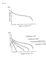
- the switching element 56 When the switching element 56 is turned off, the voltage induced in the primary side coil 55 of the switching transformer is inverted, and resonance is induced with the capacitor 57 at the same time. At this time, the drain-source voltage of the switching element 56is elevated in a sinusoidal form by the resonance phenomenon. Supposing the peak value of the drain-source voltage of the switching element 56 to be Vp, when becoming Vp > [Vz + Vbe] * R13 + R16 R16 where R13 is the resistance value of the resistance 59, and R16 is the resistance value of the resistance 60, a peak voltage control circuit 64 is put in action to effect negative feedback control to lower the voltage of the capacitor 53, thereby controlling so that Vp may be constant in every pulse of switching.
- the peak value Vp of the resonance voltage is controlled to be always constant in every pulse of switching in spite of fluctuations of the input power source 51. Accordingly, the output voltage generated in the secondary side coil 65 of the switching transformer is always constant as shown in Fig. 4, and an extremely stable voltage may be supplied to the secondary side output.
- Fig. 5 is a characteristic diagram showing the relation between the input voltage and output voltage, which shows that the output power is always kept constant as being controlled by the peak voltage control circuit 64.
- Fig. 6 is a circuit block diagram of an embodiment of the invention, being a developed example of the embodiment in Fig. 3, and explaining only the difference from the embodiment in Fig. 3, in constitution, the output of the peak voltage control circuit 64, that is, the collector of the transistor 62 is directly connected to the gate of the switching element 56, and the same effects as in the embodiment in Fig. 3 are obtained.
- Fig. 7 is a circuit block diagram of a peak voltage control circuit which is an essential component in an embodiment of the invention, and other circuit parts are same as in the circuit composition in Fig. 3.
- a comparator (or operational amplifier) 69 and a reference voltage 70 are used to compose a peak voltage control circuit 64a, and the same effects as in the embodiment in Fig. 3 are obtained.
- the control circuit is provided at the primary side, and an embodiment of installing the control circuit at the secondary side is described below.
- Fig. 8 (a) is a circuit block diagram of an embodiment of a power supply device having a control circuit provided at the secondary side, in which reference numeral 71 is a primary side power source unit composed of a DC input power source 72, a high frequency current generator 73, a primary side coil 74, and a primary side resonance capacitor 75, 76 is a secondary side power source unit composed of a secondary side coil 77, a secondary side resonance capacitor 78, an impedance variable circuit 79, a secondary side rectifier 80, and output capacitor 81, and an output detection circuit 82, and the impedance variable circuit 79 is inserted between the secondary side resonance capacitor 78 and the secondary side coil 77, and it is designed to be controlled by the output detection circuit 82 connected to both ends of the output capacitor 81.
- reference numeral 71 is a primary side power source unit composed of a DC input power source 72, a high frequency current generator 73, a primary side coil 74, and a primary side resonance capacitor 75
- 76 is a
- a high frequency current generated in the high frequency current generator 73 flows, and by this current, a high frequency voltage is generated in the primary side coil 74.
- This high frequency voltage is a sinusoidal wave owing to the resonance phenomenon of the primary side resonance capacitor 75 and the inductance of the primary side coil 74.
- the impedance When the impedance is inserted in series to the secondary side resonance capacitor 78, the characteristic of the output voltage and current is changed by the impedance as shown in Fig. 9 (b). Therefore, the output voltage or current is detected by the output detection circuit 82, and the impedance of the impedance variable circuit 79 is controlled so that it may be constant, and therefore the electric power accumulated in the secondary side resonance capacitor 78 is adjusted, and the output can be controlled at high precision.
- Fig. 8 (b) and (c) show practical examples of the impedance variable circuit 79, (b) showing a parallel circuit of transistor 83 and diode 84 and (c) using a field effect transistor 85, and Fig. 8 (d), (e), (f) show practical examples of the output detection circuit 82.
- Fig. 8 (d) is composed of a transistor 86, and resistances 87, 88 for feeding partial voltage of the output voltage to its base,(e) using a differential amplifier 89, and (f) uses an output current detection circuit for detecting the output current of a transistor 90.
- (A) denotes a terminal unit for receiving an output for control from an output voltage (current) detection circuit to the impedance variable circuit 79
- (B) shows an output terminal unit of an output voltage (current) detection circuit to the impedance variable circuit 79.
- Reference numerals 91, 92, 93 are resistances, and 89a is a reference battery for generating a reference voltage.
- Fig. 10 is a circuit diagram of an embodiment of the invention, in which the primary side composes a constant power oscillating circuit stabilized at the primary side, by connecting a primary side coil 98 of switching transformer to an AC power source 94 through a rectifying and smoothing circuit consisting of a rectifying circuit 95 and a capacitor 96, and a primary switching element 97, and connecting a control circuit 99 to the primary switching element 97.
- a transistor (FET) 101 is connected to a secondary side coil 100 through a capacitor C1, and a capacitor 103, a resistance 104, and an output terminal 105 are connected to the secondary side coil 100 of the switching transformer through a diode 102.
- output terminal 105 is connected to a transistor 106 and the transistor (FET) 101 through the resistance 104, the transistor 106 is connected from the base to a detection resistance 108 through a resistance 107, and to an output terminal 110 and a transistor 109, and the transistor (FET) 101 is connected in series to the capacitor C1, and the impedance of the transistor (FET)101 is varied, and thereby the energy transmitted to the load side is changed, so that a constant voltage and constant current control is achieved.
- the voltage obtained through the secondary side coil 100 of the switching transformer and the capacitor C1 is rectified and smoothed by the diode 102 and capacitor 103, and this output is connected to the output terminals 105, 110 through the detection resistance 108, so that the current may be always stabilized.
- a battery and others are connected to an external load 111, and the state of the external load (battery, etc.)111 is monitored by an output current changeover circuit 112, and, as shown in Fig. 11, the transistor 109 is driven, and the charging current supplied into the external load 111 is changed over to rapid charge level or trickle charge level, so that the external load 111 may be charged optimally.
- Fig. 12 shows other embodiment of the invention, which is improved from the embodiment in Fig. 10.
- constant voltage and current control is realized by varying the impedance of the transistor (FET)101, and in rapid charge, the transistor (FET) 101 is completely turned on, and a maximum output is obtained, so that a maximum power is supplied to the external load 111.
- an output characteristic diagram in Fig. 11 corresponding to curve f and curve g, it is charged by curve i (rapid charge region). At this time, the transistor 101 is turned on, and the impedance between the drain and source is small, and heat generation is kept low.
- the capacitors C2 and C3 are set appropriately so as to maintain the trickle charge region (curve c in Fig. 13).
- Fig. 14 is a circuit block diagram of a different embodiment, in which an input power source 113 is a DC voltage rectified and smoothed from a commercial power source, and a parallel circuit of primary side coil 115 and capacitor 116 is connected through a switching unit 114 to compose a primary side power supply device.
- an input power source 113 is a DC voltage rectified and smoothed from a commercial power source
- a parallel circuit of primary side coil 115 and capacitor 116 is connected through a switching unit 114 to compose a primary side power supply device.
- a secondary side power supply device 118 has a capacitor 120a and a switching element 120 connected in series to both ends of a secondary side coil 119, and a series circuit of diode 121 and capacitor 122 is connected, and an output is supplied to the load through a pulse width control unit 123, a constant voltage control unit 124, and a constant current control unit 125.
- the operation and the circuit composition are specifically described below.
- the switching unit 114 operates, and a high frequency current is supplied into the primary side coil 115.
- the primary side coil 115 resonates with the capacitor 116, and a high frequency voltage is induced.
- the voltage induced in the primary side coil 115 is further induced in the confronting secondary side coil 119, and when the switching element 120 is turned off, the secondary side coil 119 and capacitor 120ado not resonate, and only the voltage induced from the primary side coil 115 is obtained, and when the switching element 120 is turned on, the secondary side coil 119 and capacitor 120a resonate, and a high output is obtained. Still more, the resonated voltage and non-resonated voltage are averaged by the time ratio of ON period and OFF period, and rectified and smoothed by the diode 121 and capacitor 122, so that an output is obtained at both ends of the capacitor 122.
- a signal is transmitted from the constant voltage control unit 124 to the pulse width control unit 123.
- the pulse width control unit 123 is controlled by a constant frequency, and when the output voltage is lowered, the ON period of the output pulse is extended, so that it is controlled to extend the ON period of the switching element 120, that is, the ON period of the capacitor 120a, and the resonance period of the secondary side coil 119 and capacitor 120a is extended, thereby acting to raise the voltage.
- a signal is transmitted from the constant current control unit 125 to the pulse width control unit 123, and when the output current decreases, the ON period of the output pulse is extended to control to extend the ON period of the switching element 120, that is, the ON period of the capacitor 120a, and the resonance period of the secondary side coil 119 and capacitor 120a is extended, thereby acting to increase the current.
- the pulse width control unit 123 controls the on/off period of the switching pulse by the pulse width control unit 123, the on/off period of the capacitor 120a is controlled, and the output voltage and output current is controlled, so that a constant voltage and constant current output is supplied to the load.
- constant voltage control unit 124 and constant current control unit 125 may be used, depending on whether the load requires a constant voltage or a constant current.
- the first capacitor and switching element are connected in series to both ends of the coil, and the second capacitor is connected from the junction of the coil and the first capacitor through the diode, and either the constant voltage control unit or the constant current control unit is provided, and also the pulse width control unit for on/off control of the switching element by the signal from the constant voltage control unit or constant current control unit is provided, and therefore the output is obtained by on/off control of resonance of the secondary side coil 119 and capacitor 120a, not depending on analog control as in the transistor (FET) 101 in Fig. 12, and heat generation is very small, and it contributes much to downsizing of the device.
- FET transistor
- the power supply device of the invention is a power supply device capable of obtaining a stable output by controlling the primary side or controlling the secondary side.
Landscapes
- Engineering & Computer Science (AREA)
- Power Engineering (AREA)
- Dc-Dc Converters (AREA)
Applications Claiming Priority (11)
| Application Number | Priority Date | Filing Date | Title |
|---|---|---|---|
| JP11148995 | 1995-05-10 | ||
| JP11148995 | 1995-05-10 | ||
| JP13649695 | 1995-06-02 | ||
| JP13649695 | 1995-06-02 | ||
| JP14984595 | 1995-06-16 | ||
| JP14984595 | 1995-06-16 | ||
| JP22619495 | 1995-09-04 | ||
| JP22619495 | 1995-09-04 | ||
| JP22877395 | 1995-09-06 | ||
| JP22877395 | 1995-09-06 | ||
| EP96913715A EP0887912B1 (fr) | 1995-05-10 | 1996-05-09 | Alimentation electrique |
Related Parent Applications (1)
| Application Number | Title | Priority Date | Filing Date |
|---|---|---|---|
| EP96913715A Division EP0887912B1 (fr) | 1995-05-10 | 1996-05-09 | Alimentation electrique |
Publications (3)
| Publication Number | Publication Date |
|---|---|
| EP1355409A2 true EP1355409A2 (fr) | 2003-10-22 |
| EP1355409A3 EP1355409A3 (fr) | 2004-01-02 |
| EP1355409B1 EP1355409B1 (fr) | 2008-04-09 |
Family
ID=27526498
Family Applications (2)
| Application Number | Title | Priority Date | Filing Date |
|---|---|---|---|
| EP96913715A Expired - Lifetime EP0887912B1 (fr) | 1995-05-10 | 1996-05-09 | Alimentation electrique |
| EP03013345A Expired - Lifetime EP1355409B1 (fr) | 1995-05-10 | 1996-05-09 | Dispositif d'alimentation de puissance |
Family Applications Before (1)
| Application Number | Title | Priority Date | Filing Date |
|---|---|---|---|
| EP96913715A Expired - Lifetime EP0887912B1 (fr) | 1995-05-10 | 1996-05-09 | Alimentation electrique |
Country Status (8)
| Country | Link |
|---|---|
| US (1) | US5917712A (fr) |
| EP (2) | EP0887912B1 (fr) |
| JP (1) | JP3772350B2 (fr) |
| KR (1) | KR19990014663A (fr) |
| CN (1) | CN1052829C (fr) |
| CA (1) | CA2220736C (fr) |
| DE (2) | DE69637495T2 (fr) |
| WO (1) | WO1996036102A1 (fr) |
Families Citing this family (14)
| Publication number | Priority date | Publication date | Assignee | Title |
|---|---|---|---|---|
| JP2000152627A (ja) * | 1998-11-13 | 2000-05-30 | Fuji Elelctrochem Co Ltd | リンギングチョークコンバータ |
| DE19920306B4 (de) * | 1999-05-03 | 2008-02-28 | Stmicroelectronics Gmbh | Schaltungsvorrichtung zum Regeln des Stroms durch eine induktive Last |
| CN1174542C (zh) * | 1999-09-16 | 2004-11-03 | Tdk股份有限公司 | 电力变换装置的开关电路 |
| JP4314709B2 (ja) * | 1999-12-28 | 2009-08-19 | ソニー株式会社 | スイッチング電源装置 |
| JP2001224170A (ja) * | 2000-02-09 | 2001-08-17 | Sony Corp | スイッチング電源回路 |
| US6430064B1 (en) * | 2001-06-29 | 2002-08-06 | Aichi Electric Co. Ltd. | Non-contact power supply device |
| US6765809B2 (en) * | 2001-10-09 | 2004-07-20 | Samsung Electronics Co., Ltd. | Power source circuit having regulated primary current |
| JP2008005607A (ja) * | 2006-06-21 | 2008-01-10 | Matsushita Electric Works Ltd | 自励式発振回路 |
| JP4676409B2 (ja) * | 2006-10-06 | 2011-04-27 | 東光株式会社 | 非接触電力伝送装置 |
| JP5447413B2 (ja) * | 2011-03-16 | 2014-03-19 | 株式会社ダイフク | 無接触給電設備の2次側受電回路 |
| EP2761724B1 (fr) * | 2011-09-29 | 2019-12-04 | LG Innotek Co., Ltd. | Émetteur de puissance sans fil |
| DE112015000373T5 (de) * | 2014-01-10 | 2016-10-06 | Murata Manufacturing Co., Ltd. | Hochspannungsnetzgerät |
| JP7334508B2 (ja) * | 2019-07-04 | 2023-08-29 | スミダコーポレーション株式会社 | Dc/dc変換機 |
| CN113241943B (zh) * | 2021-06-23 | 2023-07-18 | 宁波奥克斯电气股份有限公司 | 输出电压控制电路、方法、控制器和家电设备 |
Citations (5)
| Publication number | Priority date | Publication date | Assignee | Title |
|---|---|---|---|---|
| GB2032719A (en) * | 1978-09-21 | 1980-05-08 | Ward Goldstone Ltd | An electronic switch and method of operating it |
| JPS58178422A (ja) * | 1982-04-14 | 1983-10-19 | Sony Corp | 電源回路 |
| US4441146A (en) * | 1982-02-04 | 1984-04-03 | Vicor Corporation | Optimal resetting of the transformer's core in single ended forward converters |
| JPH04368464A (ja) * | 1991-06-12 | 1992-12-21 | Sanyo Denki Co Ltd | 直流電源装置 |
| EP0633651A1 (fr) * | 1993-06-14 | 1995-01-11 | Vlt Corporation | Configuration, contrôle et construction de convertisseur de puissance |
Family Cites Families (13)
| Publication number | Priority date | Publication date | Assignee | Title |
|---|---|---|---|---|
| US3736496A (en) * | 1971-12-13 | 1973-05-29 | Rca Corp | Energy pump voltage regulator |
| JPS5226447B2 (fr) * | 1971-12-22 | 1977-07-14 | ||
| JPS48111827U (fr) * | 1972-03-27 | 1973-12-21 | ||
| US3989995A (en) * | 1975-05-05 | 1976-11-02 | Bell Telephone Laboratories, Incorporated | Frequency stabilized single-ended regulated converter circuit |
| JPS5226447A (en) * | 1975-08-25 | 1977-02-28 | Toshiba Corp | Grounding phase deteating apparatus |
| JPS552354A (en) * | 1978-06-20 | 1980-01-09 | Sanyo Electric Co Ltd | Power circuit |
| JPS56132177A (en) * | 1980-03-19 | 1981-10-16 | Sanyo Electric Co Ltd | High tension generation circuit |
| JPS6126302A (ja) * | 1984-07-17 | 1986-02-05 | Mitsubishi Electric Corp | 電力分配器 |
| NL8500154A (nl) * | 1985-01-22 | 1986-08-18 | Koninkl Philips Electronics Nv | Zelf-oscillerende voedingsschakeling. |
| US4937728A (en) * | 1989-03-07 | 1990-06-26 | Rca Licensing Corporation | Switch-mode power supply with burst mode standby operation |
| JPH04295284A (ja) * | 1991-03-20 | 1992-10-20 | Hiroshi Sakamoto | 電源装置 |
| JP3231498B2 (ja) * | 1993-08-03 | 2001-11-19 | 松下電器産業株式会社 | 直流電源装置 |
| US5706183A (en) * | 1994-06-27 | 1998-01-06 | Matsushita Electric Works, Ltd. | Inverter power supply with single discharge path |
-
1996
- 1996-05-09 KR KR1019970708004A patent/KR19990014663A/ko active Search and Examination
- 1996-05-09 EP EP96913715A patent/EP0887912B1/fr not_active Expired - Lifetime
- 1996-05-09 WO PCT/JP1996/001233 patent/WO1996036102A1/fr active IP Right Grant
- 1996-05-09 DE DE69637495T patent/DE69637495T2/de not_active Expired - Lifetime
- 1996-05-09 EP EP03013345A patent/EP1355409B1/fr not_active Expired - Lifetime
- 1996-05-09 DE DE69631435T patent/DE69631435T2/de not_active Expired - Fee Related
- 1996-05-09 JP JP53394696A patent/JP3772350B2/ja not_active Expired - Fee Related
- 1996-05-09 CN CN96193692A patent/CN1052829C/zh not_active Expired - Fee Related
- 1996-05-09 CA CA002220736A patent/CA2220736C/fr not_active Expired - Fee Related
- 1996-05-09 US US08/952,123 patent/US5917712A/en not_active Expired - Lifetime
Patent Citations (5)
| Publication number | Priority date | Publication date | Assignee | Title |
|---|---|---|---|---|
| GB2032719A (en) * | 1978-09-21 | 1980-05-08 | Ward Goldstone Ltd | An electronic switch and method of operating it |
| US4441146A (en) * | 1982-02-04 | 1984-04-03 | Vicor Corporation | Optimal resetting of the transformer's core in single ended forward converters |
| JPS58178422A (ja) * | 1982-04-14 | 1983-10-19 | Sony Corp | 電源回路 |
| JPH04368464A (ja) * | 1991-06-12 | 1992-12-21 | Sanyo Denki Co Ltd | 直流電源装置 |
| EP0633651A1 (fr) * | 1993-06-14 | 1995-01-11 | Vlt Corporation | Configuration, contrôle et construction de convertisseur de puissance |
Also Published As
| Publication number | Publication date |
|---|---|
| CN1183863A (zh) | 1998-06-03 |
| CN1052829C (zh) | 2000-05-24 |
| CA2220736A1 (fr) | 1996-11-14 |
| WO1996036102A1 (fr) | 1996-11-14 |
| DE69637495D1 (de) | 2008-05-21 |
| US5917712A (en) | 1999-06-29 |
| EP0887912A1 (fr) | 1998-12-30 |
| EP0887912A4 (fr) | 1999-10-06 |
| EP1355409A3 (fr) | 2004-01-02 |
| KR19990014663A (ko) | 1999-02-25 |
| DE69631435D1 (de) | 2004-03-04 |
| CA2220736C (fr) | 2004-09-28 |
| EP1355409B1 (fr) | 2008-04-09 |
| DE69637495T2 (de) | 2009-06-04 |
| DE69631435T2 (de) | 2004-11-25 |
| JP3772350B2 (ja) | 2006-05-10 |
| EP0887912B1 (fr) | 2004-01-28 |
Similar Documents
| Publication | Publication Date | Title |
|---|---|---|
| KR0147285B1 (ko) | 텔레비젼 장치의 스위치 모드 전원 공급장치 | |
| US6788556B2 (en) | Switching power source device | |
| US5917712A (en) | Self oscillating power supply | |
| US4652984A (en) | Self-oscillating power-supply circuit | |
| KR100285949B1 (ko) | 배터리 충전회로 | |
| JP3416863B2 (ja) | 電源装置 | |
| US7019992B1 (en) | Capacitively coupled power supply | |
| WO1999030409A1 (fr) | Alimentation a decoupage a limitation de courant et de tension | |
| US6525948B2 (en) | Apparatus and method for the detection of circuit irregularities and for circuit protection of a power supply | |
| JP3821156B2 (ja) | 電源装置 | |
| US5943222A (en) | Self-excited RCC type switching power supply apparatus | |
| US4965506A (en) | Power-supply circuit having circuitry for switching from a battery charging mode to a battery trickle-charging mode | |
| KR100493749B1 (ko) | 변압기 권선에 결합된 인덕터를 구비한 순방향 컨버터 | |
| US6208530B1 (en) | Switching power supply device having main switching element period control circuit | |
| US4706009A (en) | Electronic switching power supply | |
| EP0683936A1 (fr) | Circuit de commande d'un convertisseur a decoupage comprenant une technique commandee de rearmement de flux du noyau magnetique pour reguler la puissance de sortie | |
| EP0386989B1 (fr) | Alimentation à découpage avec fonctionnement en mode rafale en mode d'attente | |
| EP1463191A2 (fr) | Convertisseur à récupération autoscillante | |
| JPH09131058A (ja) | 同調スイッチ・モード電源装置 | |
| US5757629A (en) | Switched-mode power supply with compensation for varying input voltage | |
| JP4085794B2 (ja) | 電池の充電装置 | |
| JPH04229072A (ja) | 安定直流電圧発生方法並びに直流電圧源 | |
| EP0580198B1 (fr) | Circuit d'alimentation muni d'un système de veille | |
| JPH08317643A (ja) | スイッチング電源装置 | |
| WO1998011659A1 (fr) | Alimentation a decoupage a commutation a tension nulle et a commande auto-oscillante proportionnelle |
Legal Events
| Date | Code | Title | Description |
|---|---|---|---|
| PUAI | Public reference made under article 153(3) epc to a published international application that has entered the european phase |
Free format text: ORIGINAL CODE: 0009012 |
|
| 17P | Request for examination filed |
Effective date: 20030708 |
|
| AC | Divisional application: reference to earlier application |
Ref document number: 0887912 Country of ref document: EP Kind code of ref document: P |
|
| AK | Designated contracting states |
Kind code of ref document: A2 Designated state(s): DE FI FR GB SE |
|
| PUAL | Search report despatched |
Free format text: ORIGINAL CODE: 0009013 |
|
| AK | Designated contracting states |
Kind code of ref document: A3 Designated state(s): DE FI FR GB SE |
|
| RIN1 | Information on inventor provided before grant (corrected) |
Inventor name: OKURA, HIDEKI Inventor name: ONO, MAKOTO Inventor name: TSUJIMOTO, ETSUO Inventor name: HASHIMOTO, FUMIAKI |
|
| 17Q | First examination report despatched |
Effective date: 20040310 |
|
| AKX | Designation fees paid |
Designated state(s): DE FI FR GB SE |
|
| GRAP | Despatch of communication of intention to grant a patent |
Free format text: ORIGINAL CODE: EPIDOSNIGR1 |
|
| GRAS | Grant fee paid |
Free format text: ORIGINAL CODE: EPIDOSNIGR3 |
|
| GRAA | (expected) grant |
Free format text: ORIGINAL CODE: 0009210 |
|
| AC | Divisional application: reference to earlier application |
Ref document number: 0887912 Country of ref document: EP Kind code of ref document: P |
|
| AK | Designated contracting states |
Kind code of ref document: B1 Designated state(s): DE FI FR GB SE |
|
| REG | Reference to a national code |
Ref country code: GB Ref legal event code: FG4D |
|
| REF | Corresponds to: |
Ref document number: 69637495 Country of ref document: DE Date of ref document: 20080521 Kind code of ref document: P |
|
| REG | Reference to a national code |
Ref country code: SE Ref legal event code: TRGR |
|
| RAP2 | Party data changed (patent owner data changed or rights of a patent transferred) |
Owner name: PANASONIC CORPORATION |
|
| ET | Fr: translation filed | ||
| PLBE | No opposition filed within time limit |
Free format text: ORIGINAL CODE: 0009261 |
|
| STAA | Information on the status of an ep patent application or granted ep patent |
Free format text: STATUS: NO OPPOSITION FILED WITHIN TIME LIMIT |
|
| 26N | No opposition filed |
Effective date: 20090112 |
|
| PGFP | Annual fee paid to national office [announced via postgrant information from national office to epo] |
Ref country code: SE Payment date: 20090512 Year of fee payment: 14 Ref country code: FI Payment date: 20090515 Year of fee payment: 14 |
|
| REG | Reference to a national code |
Ref country code: GB Ref legal event code: 746 Effective date: 20091221 |
|
| PGFP | Annual fee paid to national office [announced via postgrant information from national office to epo] |
Ref country code: GB Payment date: 20100329 Year of fee payment: 15 |
|
| PGFP | Annual fee paid to national office [announced via postgrant information from national office to epo] |
Ref country code: FR Payment date: 20100525 Year of fee payment: 15 |
|
| PGFP | Annual fee paid to national office [announced via postgrant information from national office to epo] |
Ref country code: DE Payment date: 20100512 Year of fee payment: 15 |
|
| PG25 | Lapsed in a contracting state [announced via postgrant information from national office to epo] |
Ref country code: FI Free format text: LAPSE BECAUSE OF NON-PAYMENT OF DUE FEES Effective date: 20100509 |
|
| EUG | Se: european patent has lapsed | ||
| PG25 | Lapsed in a contracting state [announced via postgrant information from national office to epo] |
Ref country code: SE Free format text: LAPSE BECAUSE OF NON-PAYMENT OF DUE FEES Effective date: 20100510 |
|
| GBPC | Gb: european patent ceased through non-payment of renewal fee |
Effective date: 20110509 |
|
| REG | Reference to a national code |
Ref country code: FR Ref legal event code: ST Effective date: 20120131 |
|
| REG | Reference to a national code |
Ref country code: DE Ref legal event code: R119 Ref document number: 69637495 Country of ref document: DE Effective date: 20111201 |
|
| PG25 | Lapsed in a contracting state [announced via postgrant information from national office to epo] |
Ref country code: FR Free format text: LAPSE BECAUSE OF NON-PAYMENT OF DUE FEES Effective date: 20110531 |
|
| PG25 | Lapsed in a contracting state [announced via postgrant information from national office to epo] |
Ref country code: GB Free format text: LAPSE BECAUSE OF NON-PAYMENT OF DUE FEES Effective date: 20110509 |
|
| PG25 | Lapsed in a contracting state [announced via postgrant information from national office to epo] |
Ref country code: DE Free format text: LAPSE BECAUSE OF NON-PAYMENT OF DUE FEES Effective date: 20111201 |