EP1355352A2 - Stacked semiconductor device and method of manufacturing thereof - Google Patents
Stacked semiconductor device and method of manufacturing thereof Download PDFInfo
- Publication number
- EP1355352A2 EP1355352A2 EP03006051A EP03006051A EP1355352A2 EP 1355352 A2 EP1355352 A2 EP 1355352A2 EP 03006051 A EP03006051 A EP 03006051A EP 03006051 A EP03006051 A EP 03006051A EP 1355352 A2 EP1355352 A2 EP 1355352A2
- Authority
- EP
- European Patent Office
- Prior art keywords
- interposer
- semiconductor device
- semiconductor element
- semiconductor
- adhesive
- Prior art date
- Legal status (The legal status is an assumption and is not a legal conclusion. Google has not performed a legal analysis and makes no representation as to the accuracy of the status listed.)
- Withdrawn
Links
Images


Classifications
-
- H—ELECTRICITY
- H10—SEMICONDUCTOR DEVICES; ELECTRIC SOLID-STATE DEVICES NOT OTHERWISE PROVIDED FOR
- H10W—GENERIC PACKAGES, INTERCONNECTIONS, CONNECTORS OR OTHER CONSTRUCTIONAL DETAILS OF DEVICES COVERED BY CLASS H10
- H10W72/00—Interconnections or connectors in packages
-
- H—ELECTRICITY
- H10—SEMICONDUCTOR DEVICES; ELECTRIC SOLID-STATE DEVICES NOT OTHERWISE PROVIDED FOR
- H10W—GENERIC PACKAGES, INTERCONNECTIONS, CONNECTORS OR OTHER CONSTRUCTIONAL DETAILS OF DEVICES COVERED BY CLASS H10
- H10W90/00—Package configurations
-
- H—ELECTRICITY
- H10—SEMICONDUCTOR DEVICES; ELECTRIC SOLID-STATE DEVICES NOT OTHERWISE PROVIDED FOR
- H10W—GENERIC PACKAGES, INTERCONNECTIONS, CONNECTORS OR OTHER CONSTRUCTIONAL DETAILS OF DEVICES COVERED BY CLASS H10
- H10W70/00—Package substrates; Interposers; Redistribution layers [RDL]
- H10W70/60—Insulating or insulated package substrates; Interposers; Redistribution layers
-
- H—ELECTRICITY
- H10—SEMICONDUCTOR DEVICES; ELECTRIC SOLID-STATE DEVICES NOT OTHERWISE PROVIDED FOR
- H10W—GENERIC PACKAGES, INTERCONNECTIONS, CONNECTORS OR OTHER CONSTRUCTIONAL DETAILS OF DEVICES COVERED BY CLASS H10
- H10W72/00—Interconnections or connectors in packages
- H10W72/071—Connecting or disconnecting
- H10W72/072—Connecting or disconnecting of bump connectors
- H10W72/07251—Connecting or disconnecting of bump connectors characterised by changes in properties of the bump connectors during connecting
-
- H—ELECTRICITY
- H10—SEMICONDUCTOR DEVICES; ELECTRIC SOLID-STATE DEVICES NOT OTHERWISE PROVIDED FOR
- H10W—GENERIC PACKAGES, INTERCONNECTIONS, CONNECTORS OR OTHER CONSTRUCTIONAL DETAILS OF DEVICES COVERED BY CLASS H10
- H10W72/00—Interconnections or connectors in packages
- H10W72/20—Bump connectors, e.g. solder bumps or copper pillars; Dummy bumps; Thermal bumps
-
- H—ELECTRICITY
- H10—SEMICONDUCTOR DEVICES; ELECTRIC SOLID-STATE DEVICES NOT OTHERWISE PROVIDED FOR
- H10W—GENERIC PACKAGES, INTERCONNECTIONS, CONNECTORS OR OTHER CONSTRUCTIONAL DETAILS OF DEVICES COVERED BY CLASS H10
- H10W72/00—Interconnections or connectors in packages
- H10W72/50—Bond wires
- H10W72/551—Materials of bond wires
- H10W72/552—Materials of bond wires comprising metals or metalloids, e.g. silver
- H10W72/5522—Materials of bond wires comprising metals or metalloids, e.g. silver comprising gold [Au]
-
- H—ELECTRICITY
- H10—SEMICONDUCTOR DEVICES; ELECTRIC SOLID-STATE DEVICES NOT OTHERWISE PROVIDED FOR
- H10W—GENERIC PACKAGES, INTERCONNECTIONS, CONNECTORS OR OTHER CONSTRUCTIONAL DETAILS OF DEVICES COVERED BY CLASS H10
- H10W72/00—Interconnections or connectors in packages
- H10W72/851—Dispositions of multiple connectors or interconnections
- H10W72/874—On different surfaces
- H10W72/877—Bump connectors and die-attach connectors
-
- H—ELECTRICITY
- H10—SEMICONDUCTOR DEVICES; ELECTRIC SOLID-STATE DEVICES NOT OTHERWISE PROVIDED FOR
- H10W—GENERIC PACKAGES, INTERCONNECTIONS, CONNECTORS OR OTHER CONSTRUCTIONAL DETAILS OF DEVICES COVERED BY CLASS H10
- H10W72/00—Interconnections or connectors in packages
- H10W72/851—Dispositions of multiple connectors or interconnections
- H10W72/874—On different surfaces
- H10W72/884—Die-attach connectors and bond wires
-
- H—ELECTRICITY
- H10—SEMICONDUCTOR DEVICES; ELECTRIC SOLID-STATE DEVICES NOT OTHERWISE PROVIDED FOR
- H10W—GENERIC PACKAGES, INTERCONNECTIONS, CONNECTORS OR OTHER CONSTRUCTIONAL DETAILS OF DEVICES COVERED BY CLASS H10
- H10W74/00—Encapsulations, e.g. protective coatings
- H10W74/10—Encapsulations, e.g. protective coatings characterised by their shape or disposition
- H10W74/15—Encapsulations, e.g. protective coatings characterised by their shape or disposition on active surfaces of flip-chip devices, e.g. underfills
-
- H—ELECTRICITY
- H10—SEMICONDUCTOR DEVICES; ELECTRIC SOLID-STATE DEVICES NOT OTHERWISE PROVIDED FOR
- H10W—GENERIC PACKAGES, INTERCONNECTIONS, CONNECTORS OR OTHER CONSTRUCTIONAL DETAILS OF DEVICES COVERED BY CLASS H10
- H10W90/00—Package configurations
- H10W90/20—Configurations of stacked chips
- H10W90/22—Configurations of stacked chips the stacked chips being on both top and bottom sides of a package substrate, interposer or RDL
-
- H—ELECTRICITY
- H10—SEMICONDUCTOR DEVICES; ELECTRIC SOLID-STATE DEVICES NOT OTHERWISE PROVIDED FOR
- H10W—GENERIC PACKAGES, INTERCONNECTIONS, CONNECTORS OR OTHER CONSTRUCTIONAL DETAILS OF DEVICES COVERED BY CLASS H10
- H10W90/00—Package configurations
- H10W90/20—Configurations of stacked chips
- H10W90/271—Configurations of stacked chips the chips having passive surfaces facing each other, i.e. in a back-to-back arrangement
-
- H—ELECTRICITY
- H10—SEMICONDUCTOR DEVICES; ELECTRIC SOLID-STATE DEVICES NOT OTHERWISE PROVIDED FOR
- H10W—GENERIC PACKAGES, INTERCONNECTIONS, CONNECTORS OR OTHER CONSTRUCTIONAL DETAILS OF DEVICES COVERED BY CLASS H10
- H10W90/00—Package configurations
- H10W90/20—Configurations of stacked chips
- H10W90/288—Configurations of stacked chips characterised by arrangements for thermal management of the stacked chips
-
- H—ELECTRICITY
- H10—SEMICONDUCTOR DEVICES; ELECTRIC SOLID-STATE DEVICES NOT OTHERWISE PROVIDED FOR
- H10W—GENERIC PACKAGES, INTERCONNECTIONS, CONNECTORS OR OTHER CONSTRUCTIONAL DETAILS OF DEVICES COVERED BY CLASS H10
- H10W90/00—Package configurations
- H10W90/20—Configurations of stacked chips
- H10W90/297—Configurations of stacked chips characterised by the through-semiconductor vias [TSVs] in the stacked chips
-
- H—ELECTRICITY
- H10—SEMICONDUCTOR DEVICES; ELECTRIC SOLID-STATE DEVICES NOT OTHERWISE PROVIDED FOR
- H10W—GENERIC PACKAGES, INTERCONNECTIONS, CONNECTORS OR OTHER CONSTRUCTIONAL DETAILS OF DEVICES COVERED BY CLASS H10
- H10W90/00—Package configurations
- H10W90/701—Package configurations characterised by the relative positions of pads or connectors relative to package parts
- H10W90/721—Package configurations characterised by the relative positions of pads or connectors relative to package parts of bump connectors
- H10W90/722—Package configurations characterised by the relative positions of pads or connectors relative to package parts of bump connectors between stacked chips
-
- H—ELECTRICITY
- H10—SEMICONDUCTOR DEVICES; ELECTRIC SOLID-STATE DEVICES NOT OTHERWISE PROVIDED FOR
- H10W—GENERIC PACKAGES, INTERCONNECTIONS, CONNECTORS OR OTHER CONSTRUCTIONAL DETAILS OF DEVICES COVERED BY CLASS H10
- H10W90/00—Package configurations
- H10W90/701—Package configurations characterised by the relative positions of pads or connectors relative to package parts
- H10W90/721—Package configurations characterised by the relative positions of pads or connectors relative to package parts of bump connectors
- H10W90/724—Package configurations characterised by the relative positions of pads or connectors relative to package parts of bump connectors between a chip and a stacked insulating package substrate, interposer or RDL
-
- H—ELECTRICITY
- H10—SEMICONDUCTOR DEVICES; ELECTRIC SOLID-STATE DEVICES NOT OTHERWISE PROVIDED FOR
- H10W—GENERIC PACKAGES, INTERCONNECTIONS, CONNECTORS OR OTHER CONSTRUCTIONAL DETAILS OF DEVICES COVERED BY CLASS H10
- H10W90/00—Package configurations
- H10W90/701—Package configurations characterised by the relative positions of pads or connectors relative to package parts
- H10W90/731—Package configurations characterised by the relative positions of pads or connectors relative to package parts of die-attach connectors
- H10W90/732—Package configurations characterised by the relative positions of pads or connectors relative to package parts of die-attach connectors between stacked chips
-
- H—ELECTRICITY
- H10—SEMICONDUCTOR DEVICES; ELECTRIC SOLID-STATE DEVICES NOT OTHERWISE PROVIDED FOR
- H10W—GENERIC PACKAGES, INTERCONNECTIONS, CONNECTORS OR OTHER CONSTRUCTIONAL DETAILS OF DEVICES COVERED BY CLASS H10
- H10W90/00—Package configurations
- H10W90/701—Package configurations characterised by the relative positions of pads or connectors relative to package parts
- H10W90/731—Package configurations characterised by the relative positions of pads or connectors relative to package parts of die-attach connectors
- H10W90/734—Package configurations characterised by the relative positions of pads or connectors relative to package parts of die-attach connectors between a chip and a stacked insulating package substrate, interposer or RDL
-
- H—ELECTRICITY
- H10—SEMICONDUCTOR DEVICES; ELECTRIC SOLID-STATE DEVICES NOT OTHERWISE PROVIDED FOR
- H10W—GENERIC PACKAGES, INTERCONNECTIONS, CONNECTORS OR OTHER CONSTRUCTIONAL DETAILS OF DEVICES COVERED BY CLASS H10
- H10W90/00—Package configurations
- H10W90/701—Package configurations characterised by the relative positions of pads or connectors relative to package parts
- H10W90/751—Package configurations characterised by the relative positions of pads or connectors relative to package parts of bond wires
- H10W90/754—Package configurations characterised by the relative positions of pads or connectors relative to package parts of bond wires between a chip and a stacked insulating package substrate, interposer or RDL
Definitions
- the present invention generally relates to semiconductor devices and, more particularly, to a semiconductor device having a three-dimensional structure in which a plurality of semiconductor devices and semiconductor elements are stacked, and a manufacturing method of such a semiconductor device.
- the structure of the semiconductor devices has been shifting to a three-dimensional structure in which a plurality of semiconductor devices or a plurality of semiconductor elements are stacked.
- FIG. 1 is a cross-sectional view of the semiconductor device disclosed in the above-mentioned patent document.
- semiconductor chips 3 are mounted on both sides of each of interposers 1, and are encapsulated by a seal resin 2, respectively.
- the two interposers 1 are stacked with the seal resin 2, which encapsulates the semiconductor chip 3, interposed therebetween.
- the interposers 1 are connected to each other by bonding solder balls 7 to ball pads 5 which are exposed in through holes 6 formed in a solder resist 4. That is, the upper and lower interposers 1 are electrically connected to each other by the solder balls 7, and are also connect mechanically to each other.
- each semiconductor chip mounted on the stacked interposers is encapsulated by the seal resin, it is necessary to provide a distance between two interposers, which distance is greater than the thickness of the seal resin layer interposed between two interposers. Therefore, if the distance between the interposers can be reduced, the overall height of the semiconductor device can also be reduced.
- the interposers are connected and fixed to each other by the solder balls provided in the peripheral portion of the interposers, if a warp occurs in the interposers in a stacking process of an assembling process of the semiconductor package, a defect may occur in the connecting part between the interposers. Moreover, when mounting the complete semiconductor package onto a substrate, a defect may occur in the connecting part between the interposers due to a thermal deformation of the interposers and remelting of the solder balls.
- a more specific object of the present invention is to provide a semiconductor device having a three-dimensional structure in which a plurality of semiconductor devices or a plurality of semiconductor elements are stacked, the semiconductor device having a reduced overall height and an improved reliability in the mechanical strength of the stacked structure.
- Another object of the present invention is to provide a semiconductor device having a three-dimensional structure in which a plurality of semiconductor devices or a plurality of semiconductor elements are stacked, the semiconductor device having an improved heat release characteristic.
- a semiconductor device comprising: a first semiconductor element having a circuit forming surface and a back surface opposite to the circuit forming surface; a first interposer having a surface on which first electrode pads are formed and the first semiconductor element is mounted with the circuit forming surface facing the first interposer; a second semiconductor element having a circuit forming surface and a back surface opposite to the circuit forming surface; a second interposer having a surface on which second electrode pads are formed and the second semiconductor element is mounted with the circuit forming surface facing the second interposer, the second electrode pads for connection with the first interposer; and external connection terminals provided on a surface of the second interposer opposite to the surface on which the second semiconductor element is mounted, wherein the first interposer and the second interposer are electrically connected to each other by conductive members between the first and second electrode pads, and the back surface of the first semiconductor element and the back surface of the second semiconductor element are fixed to each other by an adhesive
- the first and second semiconductor elements there is no need to encapsulate the first and second semiconductor elements provided between the first and second interposers.
- a distance between the first and second interposers can be reduced, which results in a reduction in an overall thickness of the semiconductor device.
- the first and second semiconductor elements are bonded to each other by the adhesive, a mechanical strength of the connection between the interposers is improved, which prevents warp of the interposers.
- the first and second semiconductor elements are bonded to each other by the adhesive, a heat generated in the first semiconductor element can be efficiently released outside through the second semiconductor element and the second interposer.
- the semiconductor device according to the present invention may further comprise at least one third semiconductor element which is mounted on a surface of the first interposer opposite to the surface on which the first semiconductor element is mounted. Accordingly, the number of semiconductor elements stacked in the semiconductor device can be increased, which improves a packaging density. Additionally, a plurality of the third semiconductor elements may be mounted and encapsulated on the surface of the first interposer in a stacked and fixed state. Accordingly, semiconductor elements of different kinds or sizes can be efficiently arranged within the semiconductor device. Further, a metal layer for heat release may be provided on a surface of the first interposer opposite to the surface on which the first semiconductor element is mounted. Accordingly, the metal layer serves as a heat spreader, which can efficiently release a heat of the semiconductor elements to outside of the semiconductor device.
- a semiconductor device comprising: a first semiconductor element having a circuit forming surface and a back surface opposite to the circuit forming surface; a first interposer having a surface on which first electrode pads are formed and the first semiconductor element is mounted with the circuit forming surface facing the first interposer; a second semiconductor element having a circuit forming surface and a back surface opposite to the circuit forming surface; a second interposer having a surface on which second electrode pads are formed and the second semiconductor element is mounted with the circuit forming surface facing the second interposer, the second electrode pads for connection with the first interposer; and external connection terminals provided on a surface of the second interposer opposite to the surface on which the second semiconductor element is mounted, wherein the first interposer and the second interposer are electrically connected to each other by conductive members between the first and second electrode pads, and the first interposer and the back surface of the second semiconductor element are fixed to each other by an adhesive.
- the second semiconductor element provided between the first and second interposers.
- a distance between the first and second interposers can be reduced, which results in a reduction in an overall thickness of the semiconductor device.
- the second semiconductor element and the first interposer are bonded to each other by the adhesive, a mechanical strength of the connection between the interposers is improved, which prevents warp of the interposers.
- the second semiconductor element is bonded to the first interposer by the adhesive, a heat generated in the first semiconductor element can be efficiently released outside through the first interposer, the second semiconductor element and the second interposer.
- the semiconductor device according to the present invention may further comprise at least one third semiconductor element mounted on the surface of the first interposer on which the first semiconductor element is mounted. Accordingly, the number of semiconductor elements stacked in the semiconductor device can be increased, which improves a packaging density. Additionally, the semiconductor device may further comprise at least one third semiconductor element is stacked on the first semiconductor element, and the first and third semiconductor elements may be encapsulated on the first interposer.
- At least one fourth semiconductor element may be mounted on the surface of the second interposer provided with the external connection terminals.
- a plurality of the fourth semiconductor elements may be provided and encapsulated on the second interposer.
- each of the external connection terminals may be a flat pad, or may have a protruding shape.
- Each of the external connection terminals may be a lead terminal extending in a direction outward from the second interposer.
- the adhesive which bonds the back surface of the first semiconductor element and the back surface of the second semiconductor element to each other, may be a thermosetting type resin adhesive.
- the thermosetting type resin adhesive may contain at least one of silver and copper.
- a reinforcing adhesive may be provided to connecting parts between the conductive materials and the first and second interposers.
- the reinforcing adhesive may be made of an insulating thermosetting type resin material.
- the reinforcing adhesive may be in the form of a film having openings corresponding to positions of the conductive members.
- a manufacturing method of a semiconductor device comprising a first semiconductor element and a second semiconductor element, comprising the steps of: mounting the first semiconductor element onto a first interposer in a state in which a circuit forming surface of the first semiconductor element faces the first interposer; mounting the second semiconductor element onto a second interposer in a state in which a circuit forming surface of the second semiconductor element faces the second interposer; electrically connecting the first interposer and the second interposer to each other by stacking the first and second interposers with the second semiconductor element interposed therebetween and heating conductive members provided between the first and second interposers so as to melt the conductive members; and curing a thermosetting adhesive provided between a back surface of the second semiconductor device and one of a back surface of the first semiconductor element and the first interposer by a heat in the step of electrically connecting.
- FIG. 2 is a cross-sectional view of the semiconductor device according to the first embodiment of the present invention.
- the semiconductor device shown in FIG. 2 has a configuration where an interposer 1a on which a semiconductor chip 3a is mounted and an interposer 1b on which a semiconductor chip 3b is mounted are stacked.
- the interposer 1a and the interposer 1b are rearranging substrates, and are formed of a polyimide tape substrate, a glass epoxy substrate, an organic substrate (polycarbonate), etc.
- the interposer 1a and the interposer 1b are electrically connected to each other by solder balls 7, which are conductive members.
- the semiconductor chip 3a is mounted onto the interposer 1a by flip-chip-bonding, which is generally referred to as face-down mounting. That is, the semiconductor chip 3a is electrically connected to electrode pads formed on the undersurface of the interposer 1a through bumps 8 provided on the circuit forming surface of the semiconductor chip 3.
- the bumps 8 are formed of gold, copper, solder, polymer, etc.
- the semiconductor chip 3a and the interposer 1a are bonded by an under-fill adhesive 9 provided therebetween so as to be fixed to each other.
- the under-fill adhesive 9 a resin material such as epoxy, acrylics or polyimide is used.
- the semiconductor chip 3b is mounted on the interposer 1b by face-down mounting (flip-chip-bonding). That is, the semiconductor chip 3b is electrically connected to electrode pads formed on the top surface of the interposer 1b through the bumps 8 provided on the circuit forming surface of the semiconductor chip 3b.
- the semiconductor chip 3b and the interposer 1b are bonded by the under-fill adhesive 9 provided therebetween, and are fixed to each other.
- the interposer 1a and the interposer 1b are stacked with the semiconductor chips 3a and 3b interposed therebetween. Therefore, the back surfaces (a surface opposite to the circuit forming surface) of the semiconductor chips 3a and 3b are in a state where they face each other.
- the back surfaces of the semiconductor chips 3a and 3b which face each other are bonded by an adhesive 12 so that the semiconductor chips 3a and 3b are mechanically fixed to each other.
- a resin material such as epoxy, acrylics or polyimide is used for the adhesive 12, and, the resin material preferably be a thermosetting type.
- the above-mentioned resin may contain silver or copper.
- Solder balls 7A are provided as external connection terminals on the under surface of the lower interposer 1b, and parts other than the part in which the solder balls 7A are provided are covered by a solder resist 4.
- solder balls 7, which electrically connect interposer 1a and the interposer 1b, are joined to both ball pads 5a formed on the undersurface of the interposer 1a and ball pads 5b formed on the top surface of the interposer 1b. Therefore, the height of the solder balls 7 is almost equal to a height of a sum of the heights of the semiconductor chip 3a and the semiconductor chip 3b.
- the ball pads 5a and the ball pad 5b are formed as parts exposed in openings formed in the solder resist 4.
- circuit forming surface of the semiconductor chip 3a faces the interposer 1a and the under-fill adhesive 9 is filled therebetween, there is no need to encapsulate the semiconductor chip 3a by a seal resin.
- circuit forming surface of the semiconductor chip 3b faces the interposer 1b and the under-fill adhesive 9 is filled therebetween, there is no need to encapsulate the semiconductor chip 3b by a seal resin.
- the thickness of the semiconductor device according to the present embodiment can be smaller than the thickness of the conventional semiconductor device shown in FIG. 1.
- the interposer 1a and the interposer 1b are mechanically and firmly bonded by bonding the semiconductor chip 3a and the semiconductor chip 3b with the adhesive 12 in addition to the connection by the solder balls 7. Therefore, a thermal stress and an external force are prevented from concentrating into the connection parts of the solder balls 7, thereby improving the reliability of the mechanical connection between the interposers.
- the adhesive bond 12 can be cured by heating during a reflow process to join the solder balls 7 to the interposers 1a and 1b. Since the adhesive 12 is cured before the solder balls 7 melt and solidify again, the interposer 1a and the interposer 1b are fixed to each other when the solder balls 7 are cured, and, thus, the connecting positions of the solder balls cannot shift. Therefore, an accurate positioning can be achieved, and generation of a residual stress in the solder balls in the reflow process can be prevented.
- the semiconductor chip 3a is bonded to the semiconductor chip 3b by the thin layer of an adhesive 12, the heat generated within the semiconductor chip 3a is transmitted also to the lower interposer 1b through the adhesive bond 12 and the semiconductor chip 3b.
- the heat of the interposer 1b is efficiently emitted outside through the solder balls 7A. Therefore, according to the present embodiment, since a number of paths to transmit a heat from the semiconductor chip mounted on the upper interposer 1a to the lower interposer 1b is increased, the heat from the semiconductor chip can be efficiently released outside through the interposer 1b.
- the semiconductor chips 3a and 3b are mounted on the respective interposers 1a and 1b by flip-chip bonding, they may use TAB (tape automated bonding technique) as a method of carrying out face-down mounting.
- the interposers 1a and 1b are electrically connected by the solder balls 7, the bonding material and method are not limited to that disclosed.
- the connection can be made by copper post electrodes or resin balls having surfaces covered by a conductive material such as Ni/Au and the like.
- FIG. 3 is a cross-sectional view of the semiconductor device according to the second embodiment of the present invention.
- parts that are the same as the parts shown in FIG. 2 are given the same reference numerals, and descriptions thereof will be omitted.
- the semiconductor device according to the second embodiment of the present invention is configured by mounting a plurality of semiconductor chips 3c, 3d and 3e onto the top surface of the interposer shown in FIG. 2 in a stacked state.
- the semiconductor chip 3c is electrically connected to the top surface of the interposer 1a through bumps 8.
- the semiconductor chip 3c and the interposer 1a are bonded by the under-fill adhesive 9.
- the semiconductor chip 3d is mounted on the back surface of the semiconductor chip 3c in a stacked state, and is bonded to the semiconductor chip 3c by a die-bonding adhesive 10.
- a resin material such as epoxy, acrylics or polyimide can be used.
- the semiconductor chip 3d is mounted on the semiconductor chip 3c with the circuit forming surface up, and is electrically connected to the electrode pads formed on the top surface of the interposer 1a by Au wires.
- the semiconductor chip 3e is smaller than the semiconductor chip 3d, and is arranged in a stacked state in the center portion of the circuit forming surface of the semiconductor chip 3d where no electrode pad is formed.
- the semiconductor chip 3e is stacked on the semiconductor chip 3d with the circuit forming surface up, and is electrically connected to the electrode pads formed on the top surface of the interposer 1a by Au wires.
- the semiconductor chips 3c, 3d and 3e are encapsulated by the seal resin 2 on the top surface of the interposer 1a.
- the seal resin materials such as epoxy, acrylics or polyimide can be used.
- the semiconductor device according to the present embodiment can provide the same effects as the semiconductor device according to the above-mentioned first embodiment. Additionally, a heat from the semiconductor chips 3c, 3d and 3e, which are stacked on the top surface of the interposer 1a, is also transmitted to the lower interposer 1b through the semiconductor chip 3a and the semiconductor chip 3b bonded to the semiconductor chip 3a. Thereby, the heat from the semiconductor chips 3c, 3d and 3e, which are stacked on the top surface of the interposer 1a, can also be efficiently emitted outside through the lower interposer 1b.
- the present invention is not limited to the number of semiconductor chips and the method of mounting, and a different number of semiconductor chips may be mounted by a different mounting method.
- FIG. 4 is a cross-sectional view of the semiconductor device according to the third embodiment of the present invention.
- parts that are the same as the parts shown in FIG. 2 are given the same reference numerals, and descriptions thereof will be omitted.
- the semiconductor device according to the third embodiment of the present invention has a structure in which the semiconductor chip 3c is mounted on the top surface of the interposer 1a of the semiconductor device shown in FIG. 2.
- the semiconductor chip 3c is electrically connected to the top surface of the interposer 1a through bumps 8.
- the semiconductor chip 3c and the interposer 1a are bonded by the under-fill adhesive 9.
- the semiconductor chip 3c stacked on the interposer 1a is mounted with the circuit forming surface down and the under-fill adhesive 9 is filled between the circuit forming surface and the interposer 1a, there is no need to encapsulate the semiconductor chip 3c by a seal resin.
- the semiconductor chip 3b is electrically connected to the top surface of the interposer 1b through the bumps 8.
- the interposers 1a and 1b are electrically connected by the solder balls 7, and the solder balls 7A as external connection terminals are provided on the undersurface of the interposer 1b. Therefore, the semiconductor chips 3b and 3c are electrically connected to the interposer 1b through the solder balls 7, and are electrically connectable to an external circuit through the solder balls 7A serving as external connection terminals.
- the semiconductor device according to the present embodiment can provide the same effect as the semiconductor device according to the above-mentioned first embodiment. Moreover, a heat from the semiconductor chip 3c, which is stacked on the interposer 1a, can be transmitted to the lower interposer 1b through the semiconductor chip 3a mounted on the undersurface of the interposer 1a and the semiconductor chip 3b bonded to the semiconductor chip 3a. Thereby, the heat from the semiconductor chip 3c, which is mounted on the top surface of the interposer 1a, can be efficiently released outside through the interposer 1b.
- FIG. 5 is a cross-sectional view of the semiconductor device according to the fourth embodiment of the present invention.
- parts that are the same as the parts shown in FIG. 2 are given the same reference numerals, and descriptions thereof will be omitted.
- the semiconductor device has a structure in which a heat spreader 13 is provided on the top surface of the interposer 1a of the semiconductor device shown in FIG. 2.
- the heat spreader 13 for heat dissipation is formed as a metal layer formed of a material containing Cu, CuW, W, Al, AlC, Ag, etc., and is a member in the form of a sheet or a foil so as to be applied onto the top surface of the interposer 1a.
- the heat spreader 13 may be formed on the top surface of the interposer by using a wiring material such as a copper foil.
- the heat from the semiconductor chip 3a is transmitted to the semiconductor chip 3b and also to the heat spreader 13 through the interposer 1a, and, therefore, the heat from the semiconductor chip 3a can be efficiently released outside through the heat spreader 13. Additionally, when an amount of heat generated in the semiconductor chip 3b is large, the heat from the semiconductor chip 3b is transmitted to the semiconductor chip 3a and the interposer 1a, and, thus, the heat is efficiently emitted outside through the heat spreader 13.
- the configuration, the method of forming and the method of arranging of the heat spreader are not limited to the specific configuration and methods, and appropriate configuration and methods may be used if necessary.
- FIG. 6 is a cross-sectional view of the semiconductor device according to the fifth embodiment of the present invention.
- parts that are the same as the parts shown in FIG. 3 are given the same reference numerals, and descriptions thereof will be omitted.
- the semiconductor device according to the fifth embodiment of the present invention has a basic structure the same as that of the semiconductor device according to the second embodiment shown in FIG. 3, and is further provided with a semiconductor chip 3f.
- the semiconductor chip 3f is electrically connected to the undersurface of the interposer 1b through the bumps 8.
- the semiconductor chip 3f and the interposer 1b are bonded by the under-fill adhesive 9.
- solder ball 7A as external connection terminals are arranged in the circumference part of the interposer 1b, and the semiconductor chip 3f is mounted in the center portion of the under surface of the interposer 1b by flip-chip bonding. Therefore, solder balls 7A are formed so that they have a height larger than the height of the semiconductor chip 3f. According to the present embodiment, the number of stacked semiconductor chips can be increased, and, thus, the package density of semiconductor chips can be improved.
- FIG. 7 is a cross-sectional view of the semiconductor device according to the sixth embodiment of the present invention.
- parts that are the same as the parts shown in FIG. 6 are given the same reference numerals, and descriptions thereof will be omitted.
- the semiconductor device according to the sixth embodiment of the present invention has the same basic structure as the semiconductor device according to the fifth embodiment shown in FIG. 6, and is further provided with a semiconductor chip 3g.
- the semiconductor chip 3g is electrically connected to the undersurface of the interposer 1b through the Au wires 11.
- the semiconductor chip 3g is bonded to the back surface of the semiconductor chip 3f by the die bonding adhesive 10. Additionally, since the semiconductor chip 3g is connected by Au wires, the semiconductor chips 3f and 3g are integrally encapsulated by the seal resin 2 on the undersurface of the interposer 1b.
- the solder balls 7A as external connection terminals are arranged in the circumference part of the interposer 1b, and the semiconductor chips 3f and 3g are stacked and mounted on the center portion of the undersurface of the interposer 1b by flip-chip bonding. Therefore, the solder balls 7A are formed so that they have a height larger than the height of the seal resin 2. According to the present embodiment, the number of stacked semiconductor chips can be increased, and a packaging density of semiconductor chips can be improved.
- FIG. 8 is a cross-sectional view of the semiconductor device according to the seventh embodiment of the present invention.
- parts that are the same as the parts shown in FIG. 3 are given the same reference numerals, and descriptions thereof will be omitted.
- the semiconductor device according to the seventh embodiment of the present invention has a basic structure the same as the semiconductor device according to the second embodiment shown in FIG. 3, and is made as a land-grid-array (LGA) type semiconductor device. That is, although the semiconductor device according to the second embodiment shown in FIG. 3 is a ball-grid-array (BGA) type semiconductor device in which the solder balls 7A are provided on the undersurface of the interposer, the solder balls are not provided in the present embodiment and electrode pads 14 are exposed on the undersurface of the interposer 1b so that the electrode pads serve as external connection terminals.
- BGA ball-grid-array
- FIG. 9 is a cross-sectional view of the semiconductor device according to the eighth embodiment of the present invention.
- parts that are the same as the parts shown in FIG. 6 are given the same reference numerals, and descriptions thereof will be omitted.
- the semiconductor device according to the eighth embodiment of the present invention has a basic structure the same as the semiconductor device according to the fifth embodiment shown in FIG. 6, and is configured as a lead-terminal type semiconductor device.
- the semiconductor device according to the fifth embodiment shown in FIG. 6 is a semiconductor device of the BGA (ball grid array) type in which the solder balls 7A are provided on the undersurface of the interposer so as to serve as external connection terminals
- the semiconductor device according to the present embodiment is not provided with the solder balls 7A, and, instead, leads 15 are provided on the undersurface of the interposer 1b so as to serve as external connection terminals.
- FIG. 10 is a cross-sectional view of the semiconductor device according to the ninth embodiment of the present invention.
- parts that are the same as the parts shown in FIG. 3 are given the same reference numerals, and descriptions thereof will be omitted.
- the semiconductor device according to the ninth embodiment of the present invention has a basic structure the same as the semiconductor device according to the second embodiment shown in FIG. 3, and is further provided with interposers 1c and 1d.
- Semiconductor chips and solder balls are provided between the interposers 1b and 1c and between the interposers 1c and 1d in the same arrangement as the structure having the semiconductor chips 3a and 3b provided between the interposers 1a and 1b.
- the solder balls 7A serving as external connection terminals are provided on the undersurface of the lowermost interposer 1d.
- the number of the stacked semiconductor chips can be increased, and the packaging density of the semiconductor chips can be improved.
- the number of interposers and the number of semiconductor chips to be stacked are not limited to the illustrated number, and the number of semiconductor chips can be increased by increasing the number of interposers to be stacked.
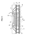
- FIG. 11 is a cross-sectional view of the semiconductor device according to the tenth embodiment of the present invention.
- parts that are the same as the parts shown in FIG. 3 are given the same reference numerals, and descriptions thereof will be omitted.
- the semiconductor device according to the tenth embodiment of the present invention has a basic structure the same as the semiconductor device according to the second embodiment shown in FIG. 3, and the connection parts of the solder balls 7 are reinforced by an adhesive 16. That is, after connecting the interposers 1a and 1b mutually with the solder balls 7, the adhesive 16 is applied around the solder balls 7 and is cured.
- an insulating resin material such as epoxy, acrylics or polyimide is used, and it is preferable to use a thermosetting type resin.
- connection parts of the solder balls 7 are reinforced by the adhesive 16
- the reliability of the connection parts is improved.
- the solder balls 7 are covered and protected by the adhesive 16, an electric short-circuit is prevented from occurring between the adjacent solder balls 7 even if, for example, a conductive foreign matter or the like enters between the interposers.
- FIG. 12 is a cross-sectional view of a semiconductor device, which is a variation of the semiconductor device shown in FIG. 11.
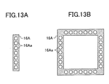
- an adhesive 16A in the form of a sheet or a film is applied on the connection parts of the solder balls 7 instead of applying the adhesive 16, which is a liquid type, and the adhesive 16A is cured by heat.
- FIGS. 13A and 13B are illustrations showing examples of the configuration of the adhesive 16A in the form of a sheet or a film.
- the adhesive 16A may be formed by a adhesive film having a stripe shape corresponding to the row of the solder balls 7, as shown in FIG. 13A, and openings 6Aa are formed beforehand in positions corresponding to the solder balls by punching using a die.
- the adhesive film 16A may be formed in the shape of a frame, as shown in FIG. 13B, and the openings 16Aa are formed in positions corresponding to the solder balls 7.
- the adhesive 16A may be placed before the solder balls 7 are subjected to reflow so that the adhesive 16A is melted and cured by the heat of the reflow.
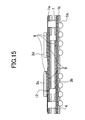
- FIG. 14 is a cross-sectional view of the semiconductor device according to the eleventh embodiment of the present invention.
- parts that are the same as the parts shown in FIG. 2 are given the same reference numerals, and descriptions thereof will be omitted.
- the semiconductor device according to the eleventh embodiment of the present invention differs from the semiconductor device according to the first embodiment shown n FIG. 2 in that only the semiconductor chip 3b is provided between the interposers 1a and 1b and the semiconductor chip 3c is mounted on the top surface of the upper interposer 1a.
- semiconductor chip 3b is mounted by flip-chip connection onto the lower interposer 1b
- the semiconductor chip 3c is mounted by flip-chip connection onto the top surface of the upper interposer 1a. Therefore, the back surface of the semiconductor chip 3b faces the under surface of the upper interposer 1a, and the back surface of the semiconductor chip 3b is bonded to the under surface of the upper interposer 1a by the adhesive 12.
- the solder balls 7 extend through inside of the through holes formed in the upper interposer 1a, and are connected to ball pads 5a of the top surface of the upper interposer 1a and ball pads 5b formed on the top surface of the lower interposer 1b.
- the thickness of the semiconductor device according to the present embodiment can be reduced.
- the back surface of the semiconductor chip 3b is fixed directly to the upper interposer 1c by the adhesive 12, similar to the above-mentioned semiconductor device according to the first embodiment shown in FIG. 2, it is prevented that a thermal stress and an external force are concentrated into the connection parts of the solder balls 7, thereby improving the reliability of the mechanical connection between the interposers.
- the adhesive 12 can be cured by heating at the time of reflow by making the adhesive 12 into a fast curable thermosetting resin. Since the adhesive 12 is cured before the solder balls 7 are melted and solidified again, the interposers 1a and 1b are fixed to each other when the solder balls are solidified, and, thus, the positions of connection of the solder balls 7 do not shift. Therefore, accurate positioning of is attained and it is prevented that a residual stress occurs in the solder balls 7 at the time of reflow.
- the interposer 1a since the interposer 1a is bonded to the semiconductor chip 3b by the thin layer of the adhesive 12, the heat generated within the semiconductor chip 3c is transmitted also to the lower interposer 1b through the interposer 1a, the adhesive bond 12 and the semiconductor chip 3b.
- the heat in the interposer 1b is efficiently released outside through the solder balls 7A. Therefore, since the number of paths to transmit the heat from the semiconductor chip mounted on the upper interposer 1a to the lower interposer 1b increases according to the present embodiment, the heat from the semiconductor chip can be efficiently released outside through the interposer 1b.
- the semiconductor chips 3b and 3c are mounted on the interposers 1a and 1b by flip-chip connection, respectively, a TAB (tape automated bonding technique) may be used as a method of face-down mounting.
- the interposers 1a and 1b are electrically connected to each other by the solder balls 7, the connection is not limited to the disclosed method.
- the interposers 1a and 1b may be connected using materials such as a copper post electrode or a resin ball having a surface covered with a conductive material such as a Ni or Au film.
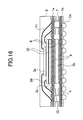
- FIG. 16 is a cross-sectional view of the semiconductor device according to the twelfth embodiment of the present invention.
- parts that are the same as the parts shown in FIG. 14 are given the same reference numerals, and descriptions thereof will be omitted.
- the semiconductor device according to the twelfth embodiment of the present invention is formed by stacking a plurality of semiconductor chips 3c, 3d and 3e on the top surface of the interposer 1a of the semiconductor device shown in FIG. 14.
- the semiconductor chip 3c is electrically connected to the top surface of the interposer 1a through the bumps 8.
- the semiconductor chip 3c and the interposer 1a are bonded by the under-fill adhesive 9.
- the semiconductor chip 3d is mounted onto the back surface of the semiconductor chip 3c, and is bonded to the semiconductor chip 3c by the die bonding adhesive 10.
- the die bonding adhesive 10 a resin material such as epoxy, acrylics or polyimide is used.
- the semiconductor chips 3d is mounted on the semiconductor chip 3c with the circuit forming surface up, and is electrically connected to electrode pads formed on the top surface of the interposer 1a by Au wires 11.
- the semiconductor chip 3e is smaller than the semiconductor chip 3d, and is arranged and stacked in the center section of the circuit forming surface of the semiconductor chip 3d in which no electrode pad is formed.
- the semiconductor chip 3e is stacked and mounted on the semiconductor chip 3d with the circuit forming surface up, and is electrically connected to the electrode pads formed on the top surface of the interposer 1a by the Au wires 11.
- the semiconductor chips 3c, 3d and 3e are encapsulated by the seal resin 2 on the top surface of the interposer 1a.
- the seal resin materials such as epoxy, acrylics or polyimide is used.
- the semiconductor device according to the present embodiment can provide the same effect as the semiconductor device according to the above-mentioned eleventh embodiment of the present invention. Moreover, the heat from the semiconductor chips 3c, 3d and 3e stacked on the top surface of the interposer 1a is transmitted to the lower interposer 1b through the semiconductor chip 3b bonded to the top surface of the interposer 1a. Thereby, the heat from the semiconductor chips 3c, 3d and 3e stacked and mounted on the top surface of the interposer 1a can also be efficiently released outside through the lower interposer 1b.
- the present invention is not limited to the number of semiconductor chips and the method of mounting semiconductor chips as explained and a different number of semiconductor chips may be stacked and mounted by a different mounting method.
- connection parts of the solder balls 7 may be reinforced by applying the adhesive 16 or 16A shown in FIG. 11 or FIG. 12 to the connection parts of the solder balls 7 having the structure shown in FIG. 14.
- the structure shown in FIG. 16 is used as a basic structure and features shown in FIG. 6 through FIG. 10 may be added.
Landscapes
- Wire Bonding (AREA)
- Cooling Or The Like Of Semiconductors Or Solid State Devices (AREA)
Abstract
Description
Claims (28)
- A semiconductor device comprising:wherein said first interposer and said second interposer are electrically connected to each other by conductive members between said first and second electrode pads, and the back surface of said first semiconductor element and the back surface of said second semiconductor element are fixed to each other by an adhesive.a first semiconductor element having a circuit forming surface and a back surface opposite to the circuit forming surface;a first interposer having a surface on which first electrode pads are formed and said first semiconductor element is mounted with the circuit forming surface facing the first interposer;a second semiconductor element having a circuit forming surface and a back surface opposite to the circuit forming surface;a second interposer having a surface on which second electrode pads are formed and said second semiconductor element is mounted with the circuit forming surface facing the second interposer, the second electrode pads for connection with said first interposer; andexternal connection terminals provided on a surface of said second interposer opposite to the surface on which said second semiconductor element is mounted,
- The semiconductor device as claimed in claim 1, further comprising at least one third semiconductor element which is mounted on a surface of said first interposer opposite to the surface on which said first semiconductor element is mounted.
- The semiconductor device as claimed in claim 2, wherein a plurality of the third semiconductor elements are mounted and encapsulated on the surface of said first interposer in a stacked and fixed state.
- The semiconductor device as claimed in claim 1, wherein a metal layer for heat release is provided on a surface of said first interposer opposite to the surface on which said first semiconductor element is mounted.
- The semiconductor device as claimed in claim 1, wherein at least one fourth semiconductor element is mounted on the surface of said second interposer provided with said external connection terminals.
- The semiconductor device as claimed in claim 5, wherein a plurality of the fourth semiconductor elements are provided and encapsulated on said second interposer.
- The semiconductor device as claimed in claim 1, wherein each of said external connection terminals is a flat pad.
- The semiconductor device as claimed in claim 1, wherein each of said external connection terminals has a protruding shape.
- The semiconductor device as claimed in claim 1, wherein each of said external connection terminals is a lead terminal extending in a direction outward from said second interposer.
- The semiconductor device as claimed in claim 1, wherein said adhesive, which bonds the back surface of said first semiconductor element and the back surface of said second semiconductor element to each other, is a thermosetting type resin adhesive.
- The semiconductor device as claimed in claim 10, wherein said thermosetting type resin adhesive contains at least one of silver and copper.
- The semiconductor device as claimed in claim 1, wherein a reinforcing adhesive is provided to connecting parts between said conductive materials and said first and second interposers.
- The semiconductor device as claimed in claim 12, wherein said reinforcing adhesive is made of an insulating thermosetting type resin material.
- The semiconductor device as claimed in claim 12, wherein said reinforcing adhesive is in the form of a film having openings corresponding to positions of said conductive members.
- A semiconductor device comprising:wherein said first interposer and said second interposer are electrically connected to each other by conductive members between said first and second electrode pads, and said first interposer and the back surface of said second semiconductor element are fixed to each other by an adhesive.a first semiconductor element having a circuit forming surface and a back surface opposite to the circuit forming surface;a first interposer having a surface on which first electrode pads are formed and said first semiconductor element is mounted with the circuit forming surface facing the first interposer;a second semiconductor element having a circuit forming surface and a back surface opposite to the circuit forming surface;a second interposer having a surface on which second electrode pads are formed and said second semiconductor element is mounted with the circuit forming surface facing the second interposer, the second electrode pads for connection with said first interposer; andexternal connection terminals provided on a surface of said second interposer opposite to the surface on which said second semiconductor element is mounted,
- The semiconductor device as claimed in claim 15, further comprising at least one third semiconductor element mounted on the surface of said first interposer on which said first semiconductor element is mounted.
- The semiconductor device as claimed in claim 15, further comprising at least one third semiconductor element is stacked on said first semiconductor element, and said first and third semiconductor elements are encapsulated on said first interposer.
- The semiconductor device as claimed in claim 15, wherein at least one fourth semiconductor element is mounted on the surface of said second interposer provided with said external connection terminals.
- The semiconductor device as claimed in claim 18, wherein a plurality of the fourth semiconductor elements are provided and encapsulated on said second interposer.
- The semiconductor device as claimed in claim 15, wherein each of said external connection terminals is a flat pad.
- The semiconductor device as claimed in claim 15, wherein each of said external connection terminals has a protruding shape.
- The semiconductor device as claimed in claim 15, wherein each of said external connection terminals is a lead terminal extending in a direction outward from said second interposer.
- The semiconductor device as claimed in claim 15, wherein said adhesive, which bonds the back surface of said first semiconductor element and the back surface of said second semiconductor element to each other, is a thermosetting type resin adhesive.
- The semiconductor device as claimed in claim 23, wherein said thermosetting type resin adhesive contains at least one of silver and copper.
- The semiconductor device as claimed in claim 15, wherein a reinforcing adhesive is provided to connecting parts between said conductive materials and said first and second interposers.
- The semiconductor device as claimed in claim 25, wherein said reinforcing adhesive is made of an insulating thermosetting type resin material.
- The semiconductor device as claimed in claim 25, wherein said reinforcing adhesive is in the form of a film having openings corresponding to positions of said conductive members.
- A manufacturing method of a semiconductor device comprising a first semiconductor element and a second semiconductor element, comprising the steps of:mounting said first semiconductor element onto a first interposer in a state in which a circuit forming surface of said first semiconductor element faces said first interposer;mounting said second semiconductor element onto a second interposer in a state in which a circuit forming surface of said second semiconductor element faces said second interposer;electrically connecting said first interposer and said second interposer to each other by stacking said first and second interposers with said second semiconductor element interposed therebetween and heating conductive members provided between said first and second interposers so as to melt the conductive members; andcuring a thermosetting adhesive provided between a back surface of said second semiconductor device and one of a back surface of said first semiconductor element and said first interposer by a heat in the step of electrically connecting.
Applications Claiming Priority (2)
| Application Number | Priority Date | Filing Date | Title |
|---|---|---|---|
| JP2002117534 | 2002-04-19 | ||
| JP2002117534A JP2003318361A (en) | 2002-04-19 | 2002-04-19 | Semiconductor device and method of manufacturing the same |
Publications (2)
| Publication Number | Publication Date |
|---|---|
| EP1355352A2 true EP1355352A2 (en) | 2003-10-22 |
| EP1355352A3 EP1355352A3 (en) | 2005-10-05 |
Family
ID=28672686
Family Applications (1)
| Application Number | Title | Priority Date | Filing Date |
|---|---|---|---|
| EP03006051A Withdrawn EP1355352A3 (en) | 2002-04-19 | 2003-03-19 | Stacked semiconductor device and method of manufacturing thereof |
Country Status (6)
| Country | Link |
|---|---|
| US (2) | US6781241B2 (en) |
| EP (1) | EP1355352A3 (en) |
| JP (1) | JP2003318361A (en) |
| KR (1) | KR20030083553A (en) |
| CN (1) | CN1452245A (en) |
| TW (1) | TW569411B (en) |
Cited By (3)
| Publication number | Priority date | Publication date | Assignee | Title |
|---|---|---|---|---|
| WO2005086234A1 (en) * | 2004-03-03 | 2005-09-15 | United Test And Assembly Center Limited | Multiple stacked die window csp package and method of manufacture |
| EP1650801A3 (en) * | 2004-10-22 | 2007-09-05 | Sun Microsystems, Inc. | Method and apparatus to facilitate capacitive communication between chips |
| CN101449377B (en) * | 2006-05-19 | 2011-04-20 | 住友电木株式会社 | Semiconductor device |
Families Citing this family (124)
| Publication number | Priority date | Publication date | Assignee | Title |
|---|---|---|---|---|
| US7247932B1 (en) * | 2000-05-19 | 2007-07-24 | Megica Corporation | Chip package with capacitor |
| USRE44438E1 (en) * | 2001-02-27 | 2013-08-13 | Stats Chippac, Ltd. | Semiconductor device and method of dissipating heat from thin package-on-package mounted to substrate |
| US8143108B2 (en) * | 2004-10-07 | 2012-03-27 | Stats Chippac, Ltd. | Semiconductor device and method of dissipating heat from thin package-on-package mounted to substrate |
| US20020121707A1 (en) * | 2001-02-27 | 2002-09-05 | Chippac, Inc. | Super-thin high speed flip chip package |
| KR100480437B1 (en) * | 2002-10-24 | 2005-04-07 | 삼성전자주식회사 | Semiconductor chip package stacked module |
| KR100701380B1 (en) * | 2002-12-30 | 2007-03-28 | 동부일렉트로닉스 주식회사 | Heat Dissipation Semiconductor Package Structure |
| JP3891123B2 (en) * | 2003-02-06 | 2007-03-14 | セイコーエプソン株式会社 | SEMICONDUCTOR DEVICE, ELECTRONIC DEVICE, ELECTRONIC DEVICE, AND SEMICONDUCTOR DEVICE MANUFACTURING METHOD |
| JP4110992B2 (en) * | 2003-02-07 | 2008-07-02 | セイコーエプソン株式会社 | Semiconductor device, electronic device, electronic apparatus, semiconductor device manufacturing method, and electronic device manufacturing method |
| JP2004259886A (en) * | 2003-02-25 | 2004-09-16 | Seiko Epson Corp | Semiconductor device, electronic device, electronic equipment, method of manufacturing semiconductor device, and method of manufacturing electronic device |
| JP3846437B2 (en) * | 2003-03-17 | 2006-11-15 | 株式会社日立製作所 | Automotive control unit |
| JP2004281818A (en) * | 2003-03-17 | 2004-10-07 | Seiko Epson Corp | Semiconductor device, electronic device, electronic device, method of manufacturing carrier substrate, method of manufacturing semiconductor device, and method of manufacturing electronic device |
| JP4069771B2 (en) * | 2003-03-17 | 2008-04-02 | セイコーエプソン株式会社 | SEMICONDUCTOR DEVICE, ELECTRONIC DEVICE, AND SEMICONDUCTOR DEVICE MANUFACTURING METHOD |
| JP2004281920A (en) * | 2003-03-18 | 2004-10-07 | Seiko Epson Corp | Semiconductor device, electronic device, electronic equipment, method of manufacturing semiconductor device, and method of manufacturing electronic device |
| JP2004281919A (en) * | 2003-03-18 | 2004-10-07 | Seiko Epson Corp | Semiconductor device, electronic device, electronic equipment, method of manufacturing semiconductor device, and method of manufacturing electronic device |
| JP3680839B2 (en) * | 2003-03-18 | 2005-08-10 | セイコーエプソン株式会社 | Semiconductor device and manufacturing method of semiconductor device |
| JP4096774B2 (en) * | 2003-03-24 | 2008-06-04 | セイコーエプソン株式会社 | SEMICONDUCTOR DEVICE, ELECTRONIC DEVICE, ELECTRONIC DEVICE, SEMICONDUCTOR DEVICE MANUFACTURING METHOD, AND ELECTRONIC DEVICE MANUFACTURING METHOD |
| JP2004349495A (en) * | 2003-03-25 | 2004-12-09 | Seiko Epson Corp | Semiconductor device, electronic device, electronic apparatus, and method of manufacturing semiconductor device |
| JP3786103B2 (en) * | 2003-05-02 | 2006-06-14 | セイコーエプソン株式会社 | SEMICONDUCTOR DEVICE, ELECTRONIC DEVICE, ELECTRONIC DEVICE, AND SEMICONDUCTOR DEVICE MANUFACTURING METHOD |
| JP3912318B2 (en) | 2003-05-02 | 2007-05-09 | セイコーエプソン株式会社 | Semiconductor device manufacturing method and electronic device manufacturing method |
| EP1636842B1 (en) | 2003-06-03 | 2011-08-17 | Casio Computer Co., Ltd. | Stackable semiconductor device and method of manufacturing the same |
| TW200504895A (en) * | 2003-06-04 | 2005-02-01 | Renesas Tech Corp | Semiconductor device |
| US7309923B2 (en) * | 2003-06-16 | 2007-12-18 | Sandisk Corporation | Integrated circuit package having stacked integrated circuits and method therefor |
| US6984881B2 (en) * | 2003-06-16 | 2006-01-10 | Sandisk Corporation | Stackable integrated circuit package and method therefor |
| JP2005072523A (en) * | 2003-08-28 | 2005-03-17 | Hitachi Ltd | Semiconductor device and manufacturing method thereof |
| US20050046034A1 (en) | 2003-09-03 | 2005-03-03 | Micron Technology, Inc. | Apparatus and method for high density multi-chip structures |
| US7180165B2 (en) * | 2003-09-05 | 2007-02-20 | Sanmina, Sci Corporation | Stackable electronic assembly |
| DE10343255B4 (en) * | 2003-09-17 | 2006-10-12 | Infineon Technologies Ag | Method for establishing electrical connections between a semiconductor chip in a BGA package and a printed circuit board |
| JP3867796B2 (en) * | 2003-10-09 | 2007-01-10 | セイコーエプソン株式会社 | Semiconductor device and manufacturing method thereof, circuit board, and electronic apparatus |
| US20050082526A1 (en) * | 2003-10-15 | 2005-04-21 | International Business Machines Corporation | Techniques for layer transfer processing |
| JP4321758B2 (en) * | 2003-11-26 | 2009-08-26 | カシオ計算機株式会社 | Semiconductor device |
| TWI278048B (en) | 2003-11-10 | 2007-04-01 | Casio Computer Co Ltd | Semiconductor device and its manufacturing method |
| KR100564585B1 (en) * | 2003-11-13 | 2006-03-28 | 삼성전자주식회사 | Dual Stacked BA Packages and Multiple Stacked BA Packages |
| JP3925809B2 (en) | 2004-03-31 | 2007-06-06 | カシオ計算機株式会社 | Semiconductor device and manufacturing method thereof |
| JP3972209B2 (en) * | 2004-05-26 | 2007-09-05 | セイコーエプソン株式会社 | Semiconductor device and manufacturing method thereof, circuit board, and electronic apparatus |
| JP4051570B2 (en) | 2004-05-26 | 2008-02-27 | セイコーエプソン株式会社 | Manufacturing method of semiconductor device |
| US6987314B1 (en) | 2004-06-08 | 2006-01-17 | Amkor Technology, Inc. | Stackable semiconductor package with solder on pads on which second semiconductor package is stacked |
| JP4865197B2 (en) * | 2004-06-30 | 2012-02-01 | ルネサスエレクトロニクス株式会社 | Semiconductor device and manufacturing method thereof |
| KR100630690B1 (en) * | 2004-07-08 | 2006-10-02 | 삼성전자주식회사 | Multichip Package with Heat Dissipation Path |
| JP4626445B2 (en) * | 2004-08-24 | 2011-02-09 | ソニー株式会社 | Manufacturing method of semiconductor package |
| CN100378993C (en) * | 2004-08-26 | 2008-04-02 | 财团法人工业技术研究院 | Three-dimensional stack formula packaging structure |
| KR100688500B1 (en) * | 2004-09-06 | 2007-03-02 | 삼성전자주식회사 | Multi-Stack Package Having Dummy Package Substrate for Semiconductor Chip Protection and Manufacturing Method Thereof |
| JP4601365B2 (en) * | 2004-09-21 | 2010-12-22 | ルネサスエレクトロニクス株式会社 | Semiconductor device |
| US20060108676A1 (en) * | 2004-11-22 | 2006-05-25 | Punzalan Nelson V Jr | Multi-chip package using an interposer |
| US7235870B2 (en) * | 2004-12-30 | 2007-06-26 | Punzalan Jr Nelson V | Microelectronic multi-chip module |
| JP2006196709A (en) * | 2005-01-13 | 2006-07-27 | Sharp Corp | Semiconductor device and manufacturing method thereof |
| US7875966B2 (en) * | 2005-02-14 | 2011-01-25 | Stats Chippac Ltd. | Stacked integrated circuit and package system |
| US7709943B2 (en) * | 2005-02-14 | 2010-05-04 | Daniel Michaels | Stacked ball grid array package module utilizing one or more interposer layers |
| US7659623B2 (en) | 2005-04-11 | 2010-02-09 | Elpida Memory, Inc. | Semiconductor device having improved wiring |
| JP2006324568A (en) * | 2005-05-20 | 2006-11-30 | Matsushita Electric Ind Co Ltd | Multilayer module and manufacturing method thereof |
| US20060267173A1 (en) * | 2005-05-26 | 2006-11-30 | Sandisk Corporation | Integrated circuit package having stacked integrated circuits and method therefor |
| US7638866B1 (en) * | 2005-06-01 | 2009-12-29 | Rockwell Collins, Inc. | Stacked packaging designs offering inherent anti-tamper protection |
| JP2006352008A (en) * | 2005-06-20 | 2006-12-28 | Nec Electronics Corp | Semiconductor device and circuit board |
| JP4551321B2 (en) * | 2005-07-21 | 2010-09-29 | 新光電気工業株式会社 | Electronic component mounting structure and manufacturing method thereof |
| US7265441B2 (en) * | 2005-08-15 | 2007-09-04 | Infineon Technologies Ag | Stackable single package and stacked multi-chip assembly |
| JP5116268B2 (en) * | 2005-08-31 | 2013-01-09 | キヤノン株式会社 | Multilayer semiconductor device and manufacturing method thereof |
| US7485969B2 (en) * | 2005-09-01 | 2009-02-03 | Micron Technology, Inc. | Stacked microelectronic devices and methods for manufacturing microelectronic devices |
| JP4473807B2 (en) * | 2005-10-27 | 2010-06-02 | パナソニック株式会社 | Multilayer semiconductor device and lower layer module of multilayer semiconductor device |
| US8409921B2 (en) * | 2006-01-12 | 2013-04-02 | Stats Chippac Ltd. | Integrated circuit package system including honeycomb molding |
| US7737539B2 (en) * | 2006-01-12 | 2010-06-15 | Stats Chippac Ltd. | Integrated circuit package system including honeycomb molding |
| US7750482B2 (en) * | 2006-02-09 | 2010-07-06 | Stats Chippac Ltd. | Integrated circuit package system including zero fillet resin |
| US7684205B2 (en) * | 2006-02-22 | 2010-03-23 | General Dynamics Advanced Information Systems, Inc. | System and method of using a compliant lead interposer |
| US7652361B1 (en) * | 2006-03-03 | 2010-01-26 | Amkor Technology, Inc. | Land patterns for a semiconductor stacking structure and method therefor |
| US8367465B2 (en) * | 2006-03-17 | 2013-02-05 | Stats Chippac Ltd. | Integrated circuit package on package system |
| JP2007287906A (en) * | 2006-04-17 | 2007-11-01 | Elpida Memory Inc | Electrode, electrode manufacturing method, and semiconductor device including the electrode |
| US20070252260A1 (en) * | 2006-04-28 | 2007-11-01 | Micron Technology, Inc. | Stacked die packages |
| US7550680B2 (en) * | 2006-06-14 | 2009-06-23 | Stats Chippac Ltd. | Package-on-package system |
| JP4901384B2 (en) * | 2006-09-14 | 2012-03-21 | パナソニック株式会社 | Resin wiring board, semiconductor device using the same, and laminated semiconductor device |
| JP2008085089A (en) * | 2006-09-28 | 2008-04-10 | Matsushita Electric Ind Co Ltd | Resin wiring board and semiconductor device |
| KR100885911B1 (en) * | 2006-11-16 | 2009-02-26 | 삼성전자주식회사 | Semiconductor package with improved heat dissipation |
| JP4917874B2 (en) * | 2006-12-13 | 2012-04-18 | 新光電気工業株式会社 | Stacked package and manufacturing method thereof |
| JP2008166440A (en) * | 2006-12-27 | 2008-07-17 | Spansion Llc | Semiconductor device |
| KR101332861B1 (en) * | 2007-01-03 | 2013-11-22 | 삼성전자주식회사 | IC package and manufacturing method |
| JP2008198916A (en) * | 2007-02-15 | 2008-08-28 | Spansion Llc | Semiconductor device and manufacturing method thereof |
| JP4751351B2 (en) * | 2007-02-20 | 2011-08-17 | 株式会社東芝 | Semiconductor device and semiconductor module using the same |
| US8124451B2 (en) * | 2007-09-21 | 2012-02-28 | Stats Chippac Ltd. | Integrated circuit packaging system with interposer |
| KR20090033605A (en) * | 2007-10-01 | 2009-04-06 | 삼성전자주식회사 | Multilayer semiconductor package, method for forming the same and electronic device having same |
| TWI415201B (en) | 2007-11-30 | 2013-11-11 | 矽品精密工業股份有限公司 | Multi-wafer stack structure and its preparation method |
| TW200931634A (en) * | 2008-01-10 | 2009-07-16 | Abounion Technology Corp | Multi-channel stacked semiconductor device and method for fabricating the same, and stacking substrate applied to the semiconductor device |
| JP5543071B2 (en) * | 2008-01-21 | 2014-07-09 | ピーエスフォー ルクスコ エスエイアールエル | Semiconductor device and semiconductor module having the same |
| TWM342699U (en) * | 2008-03-12 | 2008-10-11 | Askey Computer Corp | Wireless-signal processing circuit |
| KR100997793B1 (en) * | 2008-09-01 | 2010-12-02 | 주식회사 하이닉스반도체 | Semiconductor package and manufacturing method thereof |
| KR101198411B1 (en) * | 2008-11-17 | 2012-11-07 | 삼성전기주식회사 | package on package substrate |
| US8716868B2 (en) * | 2009-05-20 | 2014-05-06 | Panasonic Corporation | Semiconductor module for stacking and stacked semiconductor module |
| JP5271861B2 (en) | 2009-10-07 | 2013-08-21 | ルネサスエレクトロニクス株式会社 | Manufacturing method of semiconductor device |
| KR101665556B1 (en) * | 2009-11-19 | 2016-10-13 | 삼성전자 주식회사 | Semiconductor package having multi pitch ball land |
| US8476775B2 (en) * | 2009-12-17 | 2013-07-02 | Stats Chippac Ltd. | Integrated circuit packaging system with embedded interconnect and method of manufacture thereof |
| TWI416700B (en) * | 2009-12-29 | 2013-11-21 | 南茂科技股份有限公司 | Wafer stacked package structure and manufacturing method thereof |
| US9355939B2 (en) * | 2010-03-02 | 2016-05-31 | Stats Chippac Ltd. | Integrated circuit package stacking system with shielding and method of manufacture thereof |
| US8618654B2 (en) * | 2010-07-20 | 2013-12-31 | Marvell World Trade Ltd. | Structures embedded within core material and methods of manufacturing thereof |
| KR101132304B1 (en) | 2010-05-06 | 2012-04-05 | 주식회사 하이닉스반도체 | Semiconductor package and method for fabricating the same |
| US8434222B2 (en) * | 2010-08-27 | 2013-05-07 | International Business Machines Corporation | Method to manufacture a circuit apparatus having a rounded differential pair trace |
| US8304880B2 (en) * | 2010-09-14 | 2012-11-06 | Stats Chippac Ltd. | Integrated circuit packaging system with package-on-package and method of manufacture thereof |
| US8378477B2 (en) * | 2010-09-14 | 2013-02-19 | Stats Chippac Ltd. | Integrated circuit packaging system with film encapsulation and method of manufacture thereof |
| TW201230259A (en) * | 2010-09-17 | 2012-07-16 | Sumitomo Bakelite Co | A semiconductor package and a semiconductor equipment |
| US9865310B2 (en) * | 2011-02-24 | 2018-01-09 | Interconnect Systems, Inc. | High density memory modules |
| KR101740483B1 (en) * | 2011-05-02 | 2017-06-08 | 삼성전자 주식회사 | Stack Packages having a Fastening Element and a Halogen-free inter-packages connector |
| KR20130005465A (en) * | 2011-07-06 | 2013-01-16 | 삼성전자주식회사 | Semiconductor stack package apparatus |
| US9123763B2 (en) | 2011-10-12 | 2015-09-01 | Taiwan Semiconductor Manufacturing Company, Ltd. | Package-on-package (PoP) structure having at least one package comprising one die being disposed in a core material between first and second surfaces of the core material |
| US8975741B2 (en) | 2011-10-17 | 2015-03-10 | Taiwan Semiconductor Manufacturing Company, Ltd. | Process for forming package-on-package structures |
| CN105977180B (en) * | 2012-01-06 | 2020-05-08 | 日月光半导体制造股份有限公司 | Semiconductor packaging element with test structure and test method thereof |
| US8907469B2 (en) * | 2012-01-19 | 2014-12-09 | Taiwan Semiconductor Manufacturing Company, Ltd. | Integrated circuit package assembly and method of forming the same |
| JP2013243263A (en) | 2012-05-21 | 2013-12-05 | Internatl Business Mach Corp <Ibm> | Combination of power supply and heat dissipation (cooling) in three-dimensional laminate package |
| US9385006B2 (en) | 2012-06-21 | 2016-07-05 | STATS ChipPAC Pte. Ltd. | Semiconductor device and method of forming an embedded SOP fan-out package |
| CN103887263B (en) * | 2012-12-21 | 2016-12-28 | 碁鼎科技秦皇岛有限公司 | Encapsulating structure and preparation method thereof |
| WO2014171403A1 (en) * | 2013-04-17 | 2014-10-23 | ピーエスフォー ルクスコ エスエイアールエル | Semiconductor device |
| CN108321142B (en) * | 2013-07-26 | 2020-08-28 | 日月光半导体制造股份有限公司 | Semiconductor package and method of manufacturing the same |
| CN104795368B (en) * | 2014-01-17 | 2017-10-20 | 日月光半导体制造股份有限公司 | Semiconductor packaging structure and semiconductor process |
| KR102186203B1 (en) * | 2014-01-23 | 2020-12-04 | 삼성전자주식회사 | Package-on-package device including the same |
| US20150221570A1 (en) * | 2014-02-04 | 2015-08-06 | Amkor Technology, Inc. | Thin sandwich embedded package |
| JP2015216263A (en) * | 2014-05-12 | 2015-12-03 | マイクロン テクノロジー, インク. | Semiconductor device |
| CN103985695B (en) * | 2014-05-19 | 2017-07-25 | 中国科学院微电子研究所 | A fan-out packaging structure and manufacturing process thereof |
| US9355898B2 (en) | 2014-07-30 | 2016-05-31 | Qualcomm Incorporated | Package on package (PoP) integrated device comprising a plurality of solder resist layers |
| KR102341755B1 (en) | 2014-11-10 | 2021-12-23 | 삼성전자주식회사 | Semiconductor packages and methods for fabricating the same |
| KR101619455B1 (en) * | 2014-11-18 | 2016-05-11 | 주식회사 프로텍 | Method for Manufacturing Package On Package |
| KR101672622B1 (en) | 2015-02-09 | 2016-11-03 | 앰코 테크놀로지 코리아 주식회사 | Semiconductor device and manufacturing method thereof |
| JP6361821B2 (en) * | 2015-04-27 | 2018-07-25 | 富士電機株式会社 | Semiconductor device |
| US10163867B2 (en) | 2015-11-12 | 2018-12-25 | Amkor Technology, Inc. | Semiconductor package and manufacturing method thereof |
| US10068866B2 (en) * | 2016-09-29 | 2018-09-04 | Intel Corporation | Integrated circuit package having rectangular aspect ratio |
| US10636774B2 (en) | 2017-09-06 | 2020-04-28 | STATS ChipPAC Pte. Ltd. | Semiconductor device and method of forming a 3D integrated system-in-package module |
| US10468384B2 (en) | 2017-09-15 | 2019-11-05 | STATS ChipPAC Pte. Ltd. | Semiconductor device and method of forming embedded die substrate, and system-in-package modules with the same |
| US10410999B2 (en) | 2017-12-19 | 2019-09-10 | Amkor Technology, Inc. | Semiconductor device with integrated heat distribution and manufacturing method thereof |
| US10636756B2 (en) | 2018-07-05 | 2020-04-28 | STATS ChipPAC Pte. Ltd. | Semiconductor device and method of forming protrusion E-bar for 3D SIP |
| CN109065509A (en) * | 2018-08-10 | 2018-12-21 | 付伟 | Chip-packaging structure and preparation method thereof with single cofferdam and outer Mobile Communication hole |
| US11296065B2 (en) * | 2020-06-15 | 2022-04-05 | Taiwan Semiconductor Manufacturing Co., Ltd. | Semiconductor packages and methods of forming same |
Family Cites Families (10)
| Publication number | Priority date | Publication date | Assignee | Title |
|---|---|---|---|---|
| JP2856782B2 (en) * | 1989-10-12 | 1999-02-10 | レール・リキード・ソシエテ・アノニム・プール・レテユード・エ・レクスプロワタシオン・デ・プロセデ・ジョルジュ・クロード | Method of forming copper thin film by low temperature CVD |
| US5394608A (en) * | 1992-04-08 | 1995-03-07 | Hitachi Maxwell, Ltd. | Laminated semiconductor device and fabricating method thereof |
| US5247423A (en) * | 1992-05-26 | 1993-09-21 | Motorola, Inc. | Stacking three dimensional leadless multi-chip module and method for making the same |
| US6784023B2 (en) * | 1996-05-20 | 2004-08-31 | Micron Technology, Inc. | Method of fabrication of stacked semiconductor devices |
| US6225688B1 (en) * | 1997-12-11 | 2001-05-01 | Tessera, Inc. | Stacked microelectronic assembly and method therefor |
| JPH10294423A (en) * | 1997-04-17 | 1998-11-04 | Nec Corp | Semiconductor device |
| US5956233A (en) * | 1997-12-19 | 1999-09-21 | Texas Instruments Incorporated | High density single inline memory module |
| TW472330B (en) * | 1999-08-26 | 2002-01-11 | Toshiba Corp | Semiconductor device and the manufacturing method thereof |
| JP3798597B2 (en) * | 1999-11-30 | 2006-07-19 | 富士通株式会社 | Semiconductor device |
| DE10029259A1 (en) * | 2000-06-14 | 2001-12-20 | Orient Semiconductor Elect Ltd | Stack module for chips has chips on top and bottom of stacked substrates enclosed by connections between substrates |
-
2002
- 2002-04-19 JP JP2002117534A patent/JP2003318361A/en active Pending
- 2002-10-17 TW TW091123964A patent/TW569411B/en active
- 2002-10-17 US US10/272,013 patent/US6781241B2/en not_active Expired - Fee Related
- 2002-10-30 KR KR1020020066352A patent/KR20030083553A/en not_active Withdrawn
-
2003
- 2003-03-19 EP EP03006051A patent/EP1355352A3/en not_active Withdrawn
- 2003-04-17 CN CN03123119A patent/CN1452245A/en active Pending
-
2004
- 2004-04-06 US US10/817,808 patent/US6960827B2/en not_active Expired - Fee Related
Cited By (3)
| Publication number | Priority date | Publication date | Assignee | Title |
|---|---|---|---|---|
| WO2005086234A1 (en) * | 2004-03-03 | 2005-09-15 | United Test And Assembly Center Limited | Multiple stacked die window csp package and method of manufacture |
| EP1650801A3 (en) * | 2004-10-22 | 2007-09-05 | Sun Microsystems, Inc. | Method and apparatus to facilitate capacitive communication between chips |
| CN101449377B (en) * | 2006-05-19 | 2011-04-20 | 住友电木株式会社 | Semiconductor device |
Also Published As
| Publication number | Publication date |
|---|---|
| US6781241B2 (en) | 2004-08-24 |
| US20030197260A1 (en) | 2003-10-23 |
| KR20030083553A (en) | 2003-10-30 |
| JP2003318361A (en) | 2003-11-07 |
| TW569411B (en) | 2004-01-01 |
| EP1355352A3 (en) | 2005-10-05 |
| CN1452245A (en) | 2003-10-29 |
| US20040188855A1 (en) | 2004-09-30 |
| US6960827B2 (en) | 2005-11-01 |
Similar Documents
| Publication | Publication Date | Title |
|---|---|---|
| US6960827B2 (en) | Semiconductor device and manufacturing method thereof | |
| US7723839B2 (en) | Semiconductor device, stacked semiconductor device, and manufacturing method for semiconductor device | |
| JP5579402B2 (en) | Semiconductor device, method for manufacturing the same, and electronic device | |
| US6791195B2 (en) | Semiconductor device and manufacturing method of the same | |
| KR101517541B1 (en) | Multi-layer semiconductor package | |
| US6518089B2 (en) | Flip chip semiconductor device in a molded chip scale package (CSP) and method of assembly | |
| KR100856609B1 (en) | A semiconductor device and a method of manufacturing the same | |
| US6515357B2 (en) | Semiconductor package and semiconductor package fabrication method | |
| US5838061A (en) | Semiconductor package including a semiconductor chip adhesively bonded thereto | |
| JP2001077294A (en) | Semiconductor device | |
| JP2011101044A (en) | Stacked package and method of manufacturing the same | |
| KR100265566B1 (en) | Ship stack package | |
| JP2003078105A (en) | Stack chip module | |
| KR101712459B1 (en) | Method of fabricating stacked package, and method of mounting stacked package fabricated by the same | |
| JP2851609B2 (en) | Semiconductor chip package, method of manufacturing the same, and laminated package using the same | |
| US20080258286A1 (en) | High Input/Output, Low Profile Package-On-Package Semiconductor System | |
| US6992380B2 (en) | Package for semiconductor device having a device-supporting polymeric material covering a solder ball array area | |
| KR20010063236A (en) | Stack package and manufacturing method thereof | |
| US20040061239A1 (en) | Window-type ball grid array semiconductor package | |
| JP4038021B2 (en) | Manufacturing method of semiconductor device | |
| KR100443516B1 (en) | Stack package and manufacturing method thereof | |
| CN118156156A (en) | Packaging structure and forming method thereof | |
| WO2003050851A2 (en) | A semiconductor device | |
| JPWO2001018864A1 (en) | Semiconductor device and manufacturing method thereof, circuit board and electronic device |
Legal Events
| Date | Code | Title | Description |
|---|---|---|---|
| PUAI | Public reference made under article 153(3) epc to a published international application that has entered the european phase |
Free format text: ORIGINAL CODE: 0009012 |
|
| AK | Designated contracting states |
Kind code of ref document: A2 Designated state(s): AT BE BG CH CY CZ DE DK EE ES FI FR GB GR HU IE IT LI LU MC NL PT RO SE SI SK TR |
|
| AX | Request for extension of the european patent |
Extension state: AL LT LV MK |
|
| PUAL | Search report despatched |
Free format text: ORIGINAL CODE: 0009013 |
|
| AK | Designated contracting states |
Kind code of ref document: A3 Designated state(s): AT BE BG CH CY CZ DE DK EE ES FI FR GB GR HU IE IT LI LU MC NL PT RO SE SI SK TR |
|
| AX | Request for extension of the european patent |
Extension state: AL LT LV MK |
|
| 17P | Request for examination filed |
Effective date: 20060322 |
|
| AKX | Designation fees paid |
Designated state(s): DE FR IT |
|
| STAA | Information on the status of an ep patent application or granted ep patent |
Free format text: STATUS: THE APPLICATION IS DEEMED TO BE WITHDRAWN |
|
| 18D | Application deemed to be withdrawn |
Effective date: 20071002 |