EP1353382A2 - Matrice d'imagerie et son procédé de fabrication - Google Patents
Matrice d'imagerie et son procédé de fabrication Download PDFInfo
- Publication number
- EP1353382A2 EP1353382A2 EP03251941A EP03251941A EP1353382A2 EP 1353382 A2 EP1353382 A2 EP 1353382A2 EP 03251941 A EP03251941 A EP 03251941A EP 03251941 A EP03251941 A EP 03251941A EP 1353382 A2 EP1353382 A2 EP 1353382A2
- Authority
- EP
- European Patent Office
- Prior art keywords
- dielectric layer
- radiation detector
- layer
- accordance
- electrode
- Prior art date
- Legal status (The legal status is an assumption and is not a legal conclusion. Google has not performed a legal analysis and makes no representation as to the accuracy of the status listed.)
- Withdrawn
Links
- 238000000034 method Methods 0.000 title description 16
- 238000003384 imaging method Methods 0.000 title description 10
- 239000003990 capacitor Substances 0.000 claims abstract description 32
- 230000005855 radiation Effects 0.000 claims abstract description 29
- OFIYHXOOOISSDN-UHFFFAOYSA-N tellanylidenegallium Chemical compound [Te]=[Ga] OFIYHXOOOISSDN-UHFFFAOYSA-N 0.000 claims abstract description 5
- 229910021417 amorphous silicon Inorganic materials 0.000 claims description 22
- 229910052581 Si3N4 Inorganic materials 0.000 claims description 7
- HQVNEWCFYHHQES-UHFFFAOYSA-N silicon nitride Chemical compound N12[Si]34N5[Si]62N3[Si]51N64 HQVNEWCFYHHQES-UHFFFAOYSA-N 0.000 claims description 7
- AMGQUBHHOARCQH-UHFFFAOYSA-N indium;oxotin Chemical compound [In].[Sn]=O AMGQUBHHOARCQH-UHFFFAOYSA-N 0.000 claims description 2
- 239000010410 layer Substances 0.000 description 98
- 238000004519 manufacturing process Methods 0.000 description 15
- 230000000903 blocking effect Effects 0.000 description 8
- 238000002161 passivation Methods 0.000 description 8
- 239000004065 semiconductor Substances 0.000 description 8
- 238000005530 etching Methods 0.000 description 7
- 239000000463 material Substances 0.000 description 7
- 229910052782 aluminium Inorganic materials 0.000 description 6
- XAGFODPZIPBFFR-UHFFFAOYSA-N aluminium Chemical compound [Al] XAGFODPZIPBFFR-UHFFFAOYSA-N 0.000 description 6
- 239000011651 chromium Substances 0.000 description 6
- 229910052751 metal Inorganic materials 0.000 description 6
- 239000002184 metal Substances 0.000 description 6
- 238000000059 patterning Methods 0.000 description 6
- 238000000151 deposition Methods 0.000 description 5
- BHEPBYXIRTUNPN-UHFFFAOYSA-N hydridophosphorus(.) (triplet) Chemical compound [PH] BHEPBYXIRTUNPN-UHFFFAOYSA-N 0.000 description 5
- 239000000758 substrate Substances 0.000 description 5
- VYZAMTAEIAYCRO-UHFFFAOYSA-N Chromium Chemical compound [Cr] VYZAMTAEIAYCRO-UHFFFAOYSA-N 0.000 description 4
- ZOKXTWBITQBERF-UHFFFAOYSA-N Molybdenum Chemical compound [Mo] ZOKXTWBITQBERF-UHFFFAOYSA-N 0.000 description 4
- 238000003491 array Methods 0.000 description 4
- 230000004888 barrier function Effects 0.000 description 4
- 229910052804 chromium Inorganic materials 0.000 description 4
- 239000004020 conductor Substances 0.000 description 4
- 238000001465 metallisation Methods 0.000 description 4
- 229910052750 molybdenum Inorganic materials 0.000 description 4
- 239000011733 molybdenum Substances 0.000 description 4
- 239000007769 metal material Substances 0.000 description 3
- 229920002120 photoresistant polymer Polymers 0.000 description 3
- 238000001020 plasma etching Methods 0.000 description 3
- 238000004544 sputter deposition Methods 0.000 description 3
- XYFCBTPGUUZFHI-UHFFFAOYSA-N Phosphine Chemical compound P XYFCBTPGUUZFHI-UHFFFAOYSA-N 0.000 description 2
- XUIMIQQOPSSXEZ-UHFFFAOYSA-N Silicon Chemical compound [Si] XUIMIQQOPSSXEZ-UHFFFAOYSA-N 0.000 description 2
- 230000008021 deposition Effects 0.000 description 2
- 239000002019 doping agent Substances 0.000 description 2
- 238000001704 evaporation Methods 0.000 description 2
- 230000000873 masking effect Effects 0.000 description 2
- 238000000623 plasma-assisted chemical vapour deposition Methods 0.000 description 2
- 229910052710 silicon Inorganic materials 0.000 description 2
- 239000010703 silicon Substances 0.000 description 2
- 238000003860 storage Methods 0.000 description 2
- OAICVXFJPJFONN-UHFFFAOYSA-N Phosphorus Chemical compound [P] OAICVXFJPJFONN-UHFFFAOYSA-N 0.000 description 1
- VYPSYNLAJGMNEJ-UHFFFAOYSA-N Silicium dioxide Chemical compound O=[Si]=O VYPSYNLAJGMNEJ-UHFFFAOYSA-N 0.000 description 1
- 238000010521 absorption reaction Methods 0.000 description 1
- 238000000637 aluminium metallisation Methods 0.000 description 1
- 230000002238 attenuated effect Effects 0.000 description 1
- 230000015572 biosynthetic process Effects 0.000 description 1
- XQPRBTXUXXVTKB-UHFFFAOYSA-M caesium iodide Chemical compound [I-].[Cs+] XQPRBTXUXXVTKB-UHFFFAOYSA-M 0.000 description 1
- -1 cesium iodide Chemical compound 0.000 description 1
- 239000002800 charge carrier Substances 0.000 description 1
- 238000005137 deposition process Methods 0.000 description 1
- 238000002059 diagnostic imaging Methods 0.000 description 1
- 239000003989 dielectric material Substances 0.000 description 1
- 238000001312 dry etching Methods 0.000 description 1
- 230000004907 flux Effects 0.000 description 1
- 238000005755 formation reaction Methods 0.000 description 1
- 239000011229 interlayer Substances 0.000 description 1
- 230000003287 optical effect Effects 0.000 description 1
- 229910000073 phosphorus hydride Inorganic materials 0.000 description 1
- 238000000206 photolithography Methods 0.000 description 1
- 229910052814 silicon oxide Inorganic materials 0.000 description 1
- 239000000126 substance Substances 0.000 description 1
- 239000010409 thin film Substances 0.000 description 1
Images


Classifications
-
- H—ELECTRICITY
- H01—ELECTRIC ELEMENTS
- H01L—SEMICONDUCTOR DEVICES NOT COVERED BY CLASS H10
- H01L27/00—Devices consisting of a plurality of semiconductor or other solid-state components formed in or on a common substrate
- H01L27/14—Devices consisting of a plurality of semiconductor or other solid-state components formed in or on a common substrate including semiconductor components sensitive to infrared radiation, light, electromagnetic radiation of shorter wavelength or corpuscular radiation and specially adapted either for the conversion of the energy of such radiation into electrical energy or for the control of electrical energy by such radiation
- H01L27/144—Devices controlled by radiation
- H01L27/146—Imager structures
- H01L27/14643—Photodiode arrays; MOS imagers
- H01L27/14658—X-ray, gamma-ray or corpuscular radiation imagers
-
- H—ELECTRICITY
- H01—ELECTRIC ELEMENTS
- H01L—SEMICONDUCTOR DEVICES NOT COVERED BY CLASS H10
- H01L27/00—Devices consisting of a plurality of semiconductor or other solid-state components formed in or on a common substrate
- H01L27/14—Devices consisting of a plurality of semiconductor or other solid-state components formed in or on a common substrate including semiconductor components sensitive to infrared radiation, light, electromagnetic radiation of shorter wavelength or corpuscular radiation and specially adapted either for the conversion of the energy of such radiation into electrical energy or for the control of electrical energy by such radiation
Definitions
- This invention relates generally to imaging arrays, and more particularly, to pixel formations for imaging arrays.
- Imaging arrays typically include a photosensor array coupled to a scintillating medium. Radiation absorbed in the scintillator generates optical photons which in turn pass into a photosensor, such as a photodiode. The photon is absorbed in the photosensor and an electrical signal corresponding to an incident photon flux is generated.
- Hydrogenated amorphous silicon a-Si:H
- photosensitive elements such as photodiodes, can be formed in connection with necessary control or switching elements, such as thin film transistors (TFTs), in a relatively large array.
- Radiation detectors and display arrays are typically fabricated on a large substrate on which many components, including TFTs, address lines, capacitors, and devices such as photosensors, are formed through the deposition and patterning of layers of conductive, semiconductive, and insulative materials.
- At least one known fabrication process for such a TFT array typically includes fabricating a bottom gate TFT and data and scan address lines.
- the bottom gate metal shields a channel region, i.e. acts as a light blocking element, blocking light from a back light.
- the light blocking layer is desirable since photons can create an undesirable leakage in the TFT.
- the light is created from the scintillator that is deposited on the top of the devices, therefore the TFT regions are directly exposed to the photons. Therefore, an additional light blocking layer, requiring an additional photolithography level, is therefore necessary to shield the TFT channel region from undesirable light.
- a radiation detector that includes a top gate thin film transistor (TFT) including a source electrode, a drain electrode, a gate electrode, a first dielectric layer, and a second dielectric layer is provided.
- the second dielectric layer is extending over a surface of the first dielectric layer.
- the radiation detector also includes a capacitor that includes at least two electrodes and a dielectric layer. The capacitor dielectric layer is formed unitarily with the TFT second dielectric layer.
- a method for fabricating a radiation detector that includes forming a top gate thin film transistor (TFT) including a source electrode, a drain electrode, a gate electrode, a first dielectric layer, and a second dielectric layer is provided.
- the second dielectric layer is extending over a surface of the first dielectric layer.
- the method also includes forming a capacitor including at least two electrodes and a dielectric layer. The capacitor dielectric layer is formed unitarily with the TFT second dielectric layer.
- an imaging system including a radiation source and a radiation detector.
- the radiation detector includes a top gate thin film transistor (TFT) including a source electrode, a drain electrode, a gate electrode, a first dielectric layer, and a second dielectric layer.
- the second dielectric layer is extending over a surface of the first dielectric layer.
- the radiation detector also includes a capacitor including at least two electrodes and a dielectric layer. The capacitor dielectric layer is formed unitarily with the TFT second dielectric layer.
- Imaging system 10 is a medical imaging system, such as, but not limited to, a Sennovision 2000D which is commercially available from the GE Medical Systems business of General Electric Corporation, Milwaukee, Wisconsin.
- Imaging system 10 includes a radiation source 12 which projects a cone-shaped beam.
- radiation source 12 is an x-ray source 12
- the cone-shaped beam is an x-ray beam.
- the X-ray beam passes through an object 14, i.e. an object being imaged such as a patient.
- the X-ray beam after being attenuated by object 14, impinges upon radiation detector 16.
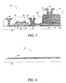
- FIG 2 is a radiation detector 18 that may be used with imaging system 10 (shown in Figure 1).
- Radiation detector 18 includes a substrate 20 on which a pixel array 22 (sometimes called a photosensor array) is disposed.
- Photosensor array 22 includes a plurality of electronic components, such as capacitors 24, photodiodes 26, and switching devices 28, such as TFTs. TFTs 28 are disposed on array 22 to selectively couple a respective capacitor 24 and photodiode 26 to a respective data line 30.
- Photosensor array 22 also includes a plurality of scan lines 32 for addressing a plurality of individual pixels 34. Data lines 30 are oriented along a first axis 36 of pixel array 22, and scan lines 32 are oriented along a second axis 38 of pixel array 22. First and second axes, 36 and 38, of pixel array 22, are disposed substantially perpendicular to each other.
- data lines 30, scan lines 32, and common lines 40 are shown extending across photosensor array 22.
- Data lines 30, scan lines 32, and common lines 40 are arranged in rows and columns such that individual pixels 34 in photosensor array 22 are addressable by one data line 30, one scan line 32, and one common line 40.
- data lines 30, scan lines 32, and common lines 40 include a conductive material, such as molybdenum, chromium, and/or aluminum.
- Capacitors 24 are electrically parallel connected to photodiodes 26, and are electrically coupled to data lines 30 through TFTs 28. Photodiodes 26 form the portion of array 22 that is responsive to incident photons and produce electric charge corresponding to a detected incident light.
- X-ray energy is converted to visible light energy by absorption in a layer of phosphor (not shown), such as cesium iodide, which is disposed near the surface of photodiodes 26.
- Capacitors 24 store a charge generated in photodiode 26 and discharge this stored charge through TFT 28 when scan line 32 is addressed. Some charge is also stored on the self-capacitance of the photo diode.
- FIG. 3 is a cross-sectional view of a portion of pixel 34 formed on substrate 20.
- Pixel 34 includes a source electrode 50, a drain electrode 52, and a first capacitor electrode 54 extending over a surface of substrate 20 such that source electrode 50, drain electrode 52, and first capacitor electrode 54 are approximately equal in thickness.
- TFT stack refers to a first dielectric layer 58 extending over a surface of a layer of semiconductive material 60, such as intrinsic amorphous silicon (a-Si). Intrinsic a-Si layer 60 is formed on and between source/drain electrodes 50, and 52. First dielectric layer 58 is formed over a-Si layer 60.
- formed includes processes to fabricate each component of pixel 34, including, but not limited to, patterning, masking, depositing, and etching. In one embodiment, an n + semiconductor layer (not shown) is formed adjacent to and on source and drain electrodes 50 and 52.
- the n + semiconductor layer can be formed by one of several methods described herein.
- the n + doped semiconductor layer is deposited, patterned, and etched to achieve the desired shape.
- a suitable material such as indium tin oxide (ITO) is used to form source and drain electrodes 50 and 52.
- ITO indium tin oxide
- the ITO is then exposed to a phosphorous plasma or other active phosphorous containing gas, prior to deposition of substantially intrinsic amorphous silicon layer 60.
- a second dielectric layer 62 is formed on first dielectric layer 58, source electrode 50, drain electrode 52, and first capacitor electrode 54.
- Second dielectric layer 62 is formed unitarily with a storage capacitor dielectric layer 64.
- a gate electrode 66 is formed unitarily with scan line 32 (shown in Figure 2), and a second capacitor electrode 68.
- a diode stack 70 is deposited on second capacitor electrode 68.
- diode stack 70 includes a PIN diode (not shown).
- a PIN diode includes a layer of p + material deposited on a layer of intrinsic a-Si which is deposited on a layer of n + material.
- a diode top contact 72 is deposited, patterned, and etched on diode stack 70.
- a passivation layer 74 is formed over diode top contact 72, diode stack 70, and exposed portions of second dielectric layer 62, gate electrode 66, and second capacitor electrode 68.
- a plurality of contact vias are then opened in the dielectric at the desired locations.
- a common via 76, a source via 78, and a drain via 80 are formed such that common via 76 is electrically connected to diode top contact 72, drain via 80 is electrically connected to drain electrode 52, and source via 78 is electrically connected to source electrode 50 and capacitor electrode 68.
- a contact via is defined as a hole in the dielectric exposing a lower conductor.
- a via is defined as the entire structure including the metal layer and the contact via hole making contact to the lower conductor.
- Figures 4 and 5 are cross-sectional views of a portion of pixel 34 shown in Figure 3 during an initial fabrication stage and a first subsequent fabrication stage respectively.
- Semiconductor and dielectric layers are deposited by plasma enhanced chemical vapor deposition (PECVD).
- PECVD plasma enhanced chemical vapor deposition
- a thin layer of n + a-Si (not shown) is deposited, patterned and etched or codeposited patterned and etched to form an n + layer on top of source/drain electrodes 50 and 52.
- the n + layer forms an ohmic electron contact and a blocking or non-injecting contact for holes.
- An ohmic contact facilitates supplying electron charge carriers to a semiconductor at a rate determined by charge transport through the semiconductor and not by the contact properties itself, therefore, current is limited by the conductivity of the semiconductor electron channel and not the contact.
- An ITO layer 90 is patterned and etched to expose source/drain electrodes 50, 52, and first capacitor electrode 54. The patterning process includes, but is not limited to, depositing a photoresist, exposing the photoresist in accordance with a desired pattern, and processing photoresist to remove portions thereof, leaving a mask having a selected pattern corresponding to desired dimensions.
- ITO layer 90 is used to form source and drain electrodes 50 and 52.
- Source electrode 50 and drain electrode 52 are selectively treated with a silicon dopant (not shown) such as, but not limited to, phosphine plasma, prior to depositing a-Si layer 60.
- Silicon dopant reacts with source electrode 50 and drain electrode 52 to selectively incorporate a phosphorous material (not shown) on the surface of source electrode 50 and drain electrode 52, and thereby modify TFTs 28 (shown in Figure 2) electrical behavior and improve ohmic contact between source/drain electrodes 50, and 52 and a-Si layer 60.
- ITO absorbs some phosphorous and subsequently liberates this phosphorous into the adjacent regions of layer 60 producing an n+ doped semiconductor layer.
- a-Si layer 60 is deposited on source electrode 50 and drain electrode 52. In one embodiment, the thickness of a-Si layer 60 is between approximately 100 angstroms( ⁇ ) and approximately 3000 ⁇ thick. In another embodiment, a-Si layer 60 is approximately 400 ⁇ . Alternatively, a-Si layer 60 is between approximately 200 ⁇ and approximately 600 ⁇ thick. First dielectric layer 58 is deposited on a-Si layer 60. In one embodiment, the thickness of first dielectric layer 58 is between approximately 100 ⁇ and approximately 500 ⁇ thick. In another embodiment, dielectric layer 58 is approximately 400 ⁇ thick. Alternatively, dielectric layer 58 is between approximately 50 ⁇ and approximately 700 ⁇ thick. First dielectric layer 60 includes, but is not limited to, SiN. First dielectric layer 58 and a-Si layer 60 are patterned and etched to form TFT stack 56. The etching process stops when ITO layer 90 is contacted.
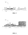
- FIG. 6 is a cross-sectional view of a portion of pixel 34 shown in Figure 3 during a second subsequent fabrication stage.
- second dielectric layer 62 is deposited on first dielectric layer 58.
- Second dielectric layer 62 such as silicon nitride (SiN), but not limited to SiN, forms storage capacitor dielectric layer 64 and also adds an additional thickness to complete a gate dielectric 92.
- second dielectric layer 62 is between approximately 500 ⁇ and approximately 3000 ⁇ thick.
- second dielectric layer 62 is approximately 2100 ⁇ thick.
- second dielectric layer 62 is between approximately 1500 ⁇ and approximately 2500 ⁇ thick.
- Second dielectric layer 62 facilitates protecting TFT stack 56 during gate metallization and diode etches that follow. Second dielectric layer 62 is not etched at this point.
- a first metallic layer 94 which facilitates blocking light from an active TFT region 96, is deposited, in a single metallization step, on second dielectric layer 62.
- Metallization is a process in which selected elements are contacted and interconnections of a plurality of circuit elements are made.
- a metallic material is deposited by sputtering or is deposited by evaporating a thin layer of a metallic material. Alternatively, the metallic material is deposited other than by sputtering or evaporating.
- First metallic layer 94 may include, but is not limited to, aluminum, chromium, and/or molybdenum.
- Figure 7 is a cross-sectional view of a portion of pixel 34 shown in Figure 3 during a third subsequent fabrication stage.
- first metallic layer 94 is patterned and etched, wherein the etching process stops when second dielectric layer 62 is contacted, to form gate electrode 66 formed unitarily with scan line 32 (shown in Figure 2) and second capacitor electrode 68.
- Gate dielectric 92 can also function as an interlayer dielectric that allows gate electrode 66 to be formed unitarily with scan line 32.
- Second capacitor electrode 68 also functions as a diode bottom contact.
- Gate electrode 66 and second capacitor electrode 68 may include, but are not limited to, molybdenum, aluminum, and/or chromium, and are deposited in a sputtering process to a thickness of approximately 2000 ⁇ .
- scan line 32 is a molybdenum/chromium (Mo/Cr) stack wherein a relatively thin layer of Cr (approximately 300 ⁇ ) is an etch stop for reactive ion etching (RIE) diode stack 70.
- RIE reactive ion etching
- diode stack 70 is deposited on second capacitor electrode 68 without any intervening patterning step.
- Diode top contact 72 formed from a transparent conductor such as ITO, is deposited on diode stack 70.
- Diode stack 70 is patterned and etched. The same mask may be used to first wet etch, or alternatively, dry etch diode top contact 72, followed by a dry etching of diode stack 70. Alternatively, two separate masking steps can be used to define diode top contact 72, smaller than diode stack 70, followed by patterning and etching diode stack 70.
- Figure 8 is a cross-sectional view of a portion of pixel 34 shown in Figure 3 during a fourth subsequent fabrication stage.
- passivation layer 74 is deposited over pixel 34.
- Passivation layer 74 is etched to expose diode top contact 72, second capacitor electrode 68, source electrode 50, drain electrode 52, and gate electrode 66.
- Passivation layer 74 is relatively thick, between 0.2 microns ( ⁇ ) to 1.0 ⁇ and may be formed from material such as, but not limited to, silicon nitride and silicon oxide.
- Passivation layer 74 facilitates protecting a plurality of diode sidewalls 97 (shown in Figure 7) against mechanical and chemical damage in subsequent processing.
- a second metallic layer 98 is deposited on pixel 34 to form common via 76, source via 78, and drain via 80 in passivation layer 74.
- the source via 78 and drain via 80 are etched through two different thicknesses of dielectric material.
- Common via 76, source via 78, and drain via 80 are formed in one etching step to provide access through a portion of passivation layer 74 (i.e. common via 76, source via 78, and drain via 80 are surrounded on all sides by remaining portions of common passivation layer 74) such that electrical contact can be made to underlying components.
- pixel 34 can be fabricated in the processing steps described herein, and allows aluminum metallization, which is desirable for low resistance lines.
- Metallic gate 66 does not contact a-Si layer 60 directly so no special processes or barrier metal is used in the process.
- second metallic layer 98 forms data line 30 (shown in Figure 2) and common electrode 76, and can be formed from aluminum. Second metallic layer 98 is also not in contact with a-Si layer 60 such that no special processes or barrier metal is required. Also, no high temperature processes follows the aluminum deposition process, reducing the chance of forming aluminum hillocks (not shown), which may cause shorts.
- a barrier dielectric layer (not shown) is deposited over pixel 34, patterned and etched, to expose contact pads (not shown).
- the barrier dielectric layer may include, but is not limited to silicon nitride.
- Inverting the TFT structure to form a top gate staggered structure as describe herein facilitates blocking light from the active TFT regions since the gate metal serves as both the gate of the TFT and also as a light blocking layer for the channel region.
Landscapes
- Engineering & Computer Science (AREA)
- Power Engineering (AREA)
- Physics & Mathematics (AREA)
- General Physics & Mathematics (AREA)
- Electromagnetism (AREA)
- Condensed Matter Physics & Semiconductors (AREA)
- Computer Hardware Design (AREA)
- Microelectronics & Electronic Packaging (AREA)
- Health & Medical Sciences (AREA)
- Toxicology (AREA)
- Solid State Image Pick-Up Elements (AREA)
- Light Receiving Elements (AREA)
- Measurement Of Radiation (AREA)
- Transforming Light Signals Into Electric Signals (AREA)
- Thin Film Transistor (AREA)
Applications Claiming Priority (2)
| Application Number | Priority Date | Filing Date | Title |
|---|---|---|---|
| US10/116,469 US6740884B2 (en) | 2002-04-03 | 2002-04-03 | Imaging array and methods for fabricating same |
| US116469 | 2002-04-03 |
Publications (2)
| Publication Number | Publication Date |
|---|---|
| EP1353382A2 true EP1353382A2 (fr) | 2003-10-15 |
| EP1353382A3 EP1353382A3 (fr) | 2003-11-26 |
Family
ID=28453935
Family Applications (1)
| Application Number | Title | Priority Date | Filing Date |
|---|---|---|---|
| EP03251941A Withdrawn EP1353382A3 (fr) | 2002-04-03 | 2003-03-27 | Matrice d'imagerie et son procédé de fabrication |
Country Status (4)
| Country | Link |
|---|---|
| US (1) | US6740884B2 (fr) |
| EP (1) | EP1353382A3 (fr) |
| JP (1) | JP4484440B2 (fr) |
| KR (1) | KR20030082379A (fr) |
Cited By (3)
| Publication number | Priority date | Publication date | Assignee | Title |
|---|---|---|---|---|
| EP2178123A2 (fr) * | 2008-10-14 | 2010-04-21 | Dpix Llc | Conception de réduction d'artéfact induit à ESD pour un réseau de capteur d'image de transistor à couche mince |
| WO2016025463A1 (fr) * | 2014-08-15 | 2016-02-18 | Perkinelmer Holdings, Inc. | Dispositif d'imagerie par rayonnement avec photodétecteur métal-isolant-semi-conducteur et transistor en couches minces |
| CN109417080A (zh) * | 2018-09-26 | 2019-03-01 | 深圳市汇顶科技股份有限公司 | 光学图像采集单元、光学图像采集装置和电子设备 |
Families Citing this family (29)
| Publication number | Priority date | Publication date | Assignee | Title |
|---|---|---|---|---|
| TW544946B (en) * | 2002-07-12 | 2003-08-01 | Hannstar Display Corp | Manufacturing method of X-ray inspecting instrument array unit |
| US7145152B2 (en) * | 2003-10-14 | 2006-12-05 | General Electric Company | Storage capacitor design for a solid state imager |
| US6982176B2 (en) * | 2003-10-30 | 2006-01-03 | General Electric Company | Method for monitoring production of pixel detectors and detectors produced thereby |
| US7105828B2 (en) * | 2004-02-10 | 2006-09-12 | Ge Medical Systems Global Technology Company, Llc | Hybrid x-ray detector |
| US7521298B2 (en) * | 2006-11-25 | 2009-04-21 | Wintec Corporation | Thin film transistor array panel of active liquid crystal display and fabrication method thereof |
| JP5286691B2 (ja) * | 2007-05-14 | 2013-09-11 | 三菱電機株式会社 | フォトセンサー |
| KR101218089B1 (ko) * | 2007-12-07 | 2013-01-18 | 엘지디스플레이 주식회사 | 디지털 엑스레이 디텍터 및 그 제조방법 |
| EP2230934B8 (fr) | 2007-12-14 | 2012-10-24 | AeroDesigns, Inc | Administration de produits alimentaires sous forme d'aérosols |
| JP2010205987A (ja) * | 2009-03-04 | 2010-09-16 | Sony Corp | 薄膜トランジスタおよびその製造方法並びに表示装置 |
| JP5402211B2 (ja) * | 2009-04-27 | 2014-01-29 | セイコーエプソン株式会社 | 光電変換装置の製造方法 |
| TWI424574B (zh) * | 2009-07-28 | 2014-01-21 | Prime View Int Co Ltd | 數位x光探測面板及其製作方法 |
| WO2012043908A1 (fr) * | 2010-09-30 | 2012-04-05 | (주)디알텍 | Détecteur de rayonnement et procédé de détection de rayonnement |
| KR101217808B1 (ko) | 2010-09-30 | 2013-01-21 | 주식회사 디알텍 | 방사선 검출기 및 방사선 검출 방법 |
| KR101322331B1 (ko) * | 2011-05-26 | 2013-10-28 | 전자부품연구원 | X-ray 검출기용 박막 트랜지스터 어레이 기판 및 상기 기판에 구비된 박막 트랜지스터의 제조 방법 |
| US8878137B2 (en) * | 2011-10-13 | 2014-11-04 | Varian Medical Systems, Inc. | Photo detector of an X-ray imager |
| US20130240875A1 (en) * | 2012-03-14 | 2013-09-19 | Semiconductor Energy Laboratory Co., Ltd. | Semiconductor device and method for manufacturing the same |
| CN102629610A (zh) * | 2012-03-27 | 2012-08-08 | 北京京东方光电科技有限公司 | 一种x射线检测装置的阵列基板及其制造方法 |
| CN102664184B (zh) * | 2012-03-27 | 2014-08-06 | 北京京东方光电科技有限公司 | 一种x射线检测装置的阵列基板的制造方法 |
| CN102800750B (zh) * | 2012-07-26 | 2015-07-01 | 北京京东方光电科技有限公司 | 一种传感器的制造方法 |
| KR101965259B1 (ko) * | 2012-07-27 | 2019-08-08 | 삼성디스플레이 주식회사 | 엑스선 검출기 |
| TWI496277B (zh) * | 2012-12-03 | 2015-08-11 | Innocom Tech Shenzhen Co Ltd | X光偵測裝置 |
| CN103474474B (zh) * | 2013-09-16 | 2016-08-17 | 北京京东方光电科技有限公司 | Tft及其制作方法、阵列基板及其制作方法、x射线探测器 |
| US9917133B2 (en) | 2013-12-12 | 2018-03-13 | General Electric Company | Optoelectronic device with flexible substrate |
| EP3117204B1 (fr) | 2014-03-13 | 2021-06-16 | General Electric Company | Détecteur numérique à rayons x incurvé pour inspection de soudure |
| CN105304656B (zh) * | 2014-06-23 | 2018-06-22 | 上海箩箕技术有限公司 | 光电传感器 |
| KR102603411B1 (ko) * | 2017-12-18 | 2023-11-16 | 엘지디스플레이 주식회사 | 마이크로led 표시장치 |
| CN110047859A (zh) * | 2019-04-24 | 2019-07-23 | 北京京东方传感技术有限公司 | 传感器及其制备方法 |
| US11846739B2 (en) * | 2021-01-12 | 2023-12-19 | Innocare Optoelectronics Corporation | Circuit for sensing X-ray |
| CN113224100A (zh) * | 2021-05-25 | 2021-08-06 | 信利半导体有限公司 | 一种非晶氧化物薄膜晶体管光学感应器及电子设备 |
Citations (5)
| Publication number | Priority date | Publication date | Assignee | Title |
|---|---|---|---|---|
| US5196721A (en) * | 1989-10-03 | 1993-03-23 | Fuji Xerox Co., Ltd. | Image reading device |
| EP0555907A1 (fr) * | 1992-02-08 | 1993-08-18 | Philips Electronics Uk Limited | Procédé de fabrication d'un réseau à matrices actives à grande surface |
| US5917199A (en) * | 1998-05-15 | 1999-06-29 | Ois Optical Imaging Systems, Inc. | Solid state imager including TFTS with variably doped contact layer system for reducing TFT leakage current and increasing mobility and method of making same |
| US5942310A (en) * | 1995-09-12 | 1999-08-24 | Lg Electronics Inc. | Liquid crystal display with increased aperture ratio |
| US20010005598A1 (en) | 1999-12-15 | 2001-06-28 | U.S. Philips Corporation | Method of manufacturing an active matrix device |
Family Cites Families (33)
| Publication number | Priority date | Publication date | Assignee | Title |
|---|---|---|---|---|
| US4739414A (en) | 1986-07-15 | 1988-04-19 | Ovonic Imaging Systems, Inc. | Large area array of thin film photosensitive elements for image detection |
| US4725890A (en) | 1986-07-15 | 1988-02-16 | Ovonic Imaging Systems, Inc. | Flexible array of photosensitive elements |
| US4889983A (en) | 1987-11-24 | 1989-12-26 | Mitsubishi Denki Kabushiki Kaisha | Image sensor and production method thereof |
| JPH0423470A (ja) | 1990-05-18 | 1992-01-27 | Fuji Xerox Co Ltd | イメージセンサ |
| US5254480A (en) | 1992-02-20 | 1993-10-19 | Minnesota Mining And Manufacturing Company | Process for producing a large area solid state radiation detector |
| GB9209734D0 (en) * | 1992-05-06 | 1992-06-17 | Philips Electronics Uk Ltd | An image sensor |
| JPH0772510A (ja) * | 1993-09-07 | 1995-03-17 | Hitachi Ltd | アクティブマトリクス型液晶表示装置 |
| US5399884A (en) | 1993-11-10 | 1995-03-21 | General Electric Company | Radiation imager with single passivation dielectric for transistor and diode |
| US5587591A (en) | 1993-12-29 | 1996-12-24 | General Electric Company | Solid state fluoroscopic radiation imager with thin film transistor addressable array |
| US5435608A (en) | 1994-06-17 | 1995-07-25 | General Electric Company | Radiation imager with common passivation dielectric for gate electrode and photosensor |
| US5517031A (en) * | 1994-06-21 | 1996-05-14 | General Electric Company | Solid state imager with opaque layer |
| DE69424805T2 (de) | 1994-07-27 | 2000-12-07 | 1294339 Ontario Inc | Bildwandlersystem |
| US5532180A (en) | 1995-06-02 | 1996-07-02 | Ois Optical Imaging Systems, Inc. | Method of fabricating a TFT with reduced channel length |
| US6124606A (en) * | 1995-06-06 | 2000-09-26 | Ois Optical Imaging Systems, Inc. | Method of making a large area imager with improved signal-to-noise ratio |
| US5614727A (en) | 1995-06-06 | 1997-03-25 | International Business Machines Corporation | Thin film diode having large current capability with low turn-on voltages for integrated devices |
| US5631473A (en) | 1995-06-21 | 1997-05-20 | General Electric Company | Solid state array with supplemental dielectric layer crossover structure |
| EP0762505A3 (fr) | 1995-08-28 | 1999-02-03 | Canon Kabushiki Kaisha | Appareil pour la détection de radiation et procédé de fabrication d'un tel appareil |
| US5610403A (en) | 1995-09-05 | 1997-03-11 | General Electric Company | Solid state radiation imager with gate electrode plane shield wires |
| US5610404A (en) | 1995-09-05 | 1997-03-11 | General Electric Company | Flat panel imaging device with ground plane electrode |
| US5648654A (en) | 1995-12-21 | 1997-07-15 | General Electric Company | Flat panel imaging device with patterned common electrode |
| US5777355A (en) | 1996-12-23 | 1998-07-07 | General Electric Company | Radiation imager with discontinuous dielectric |
| US5920070A (en) | 1996-11-27 | 1999-07-06 | General Electric Company | Solid state area x-ray detector with adjustable bias |
| JP3729953B2 (ja) * | 1996-12-02 | 2005-12-21 | コーニンクレッカ フィリップス エレクトロニクス エヌ ヴィ | Tftアレイ基板とその製法 |
| US5838054A (en) | 1996-12-23 | 1998-11-17 | General Electric Company | Contact pads for radiation imagers |
| US5736732A (en) | 1996-12-23 | 1998-04-07 | General Electric Company | Induced charge prevention in semiconductor imaging devices |
| JP3784491B2 (ja) * | 1997-03-28 | 2006-06-14 | 株式会社半導体エネルギー研究所 | アクティブマトリクス型の表示装置 |
| US6167110A (en) | 1997-11-03 | 2000-12-26 | General Electric Company | High voltage x-ray and conventional radiography imaging apparatus and method |
| US6031234A (en) | 1997-12-08 | 2000-02-29 | General Electric Company | High resolution radiation imager |
| US6025599A (en) | 1997-12-09 | 2000-02-15 | Direct Radiography Corp. | Image capture element |
| US6060714A (en) * | 1998-01-23 | 2000-05-09 | Ois Optical Imaging Systems, Inc. | Large area imager with photo-imageable interface barrier layer |
| US6075248A (en) * | 1998-10-22 | 2000-06-13 | Direct Radiography Corp. | Direct radiographic imaging panel with shielding electrode |
| US6243441B1 (en) | 1999-07-13 | 2001-06-05 | Edge Medical Devices | Active matrix detector for X-ray imaging |
| US6559506B1 (en) * | 2002-04-03 | 2003-05-06 | General Electric Company | Imaging array and methods for fabricating same |
-
2002
- 2002-04-03 US US10/116,469 patent/US6740884B2/en not_active Expired - Lifetime
-
2003
- 2003-03-27 EP EP03251941A patent/EP1353382A3/fr not_active Withdrawn
- 2003-04-02 JP JP2003098710A patent/JP4484440B2/ja not_active Expired - Lifetime
- 2003-04-02 KR KR10-2003-0020676A patent/KR20030082379A/ko not_active Application Discontinuation
Patent Citations (5)
| Publication number | Priority date | Publication date | Assignee | Title |
|---|---|---|---|---|
| US5196721A (en) * | 1989-10-03 | 1993-03-23 | Fuji Xerox Co., Ltd. | Image reading device |
| EP0555907A1 (fr) * | 1992-02-08 | 1993-08-18 | Philips Electronics Uk Limited | Procédé de fabrication d'un réseau à matrices actives à grande surface |
| US5942310A (en) * | 1995-09-12 | 1999-08-24 | Lg Electronics Inc. | Liquid crystal display with increased aperture ratio |
| US5917199A (en) * | 1998-05-15 | 1999-06-29 | Ois Optical Imaging Systems, Inc. | Solid state imager including TFTS with variably doped contact layer system for reducing TFT leakage current and increasing mobility and method of making same |
| US20010005598A1 (en) | 1999-12-15 | 2001-06-28 | U.S. Philips Corporation | Method of manufacturing an active matrix device |
Cited By (5)
| Publication number | Priority date | Publication date | Assignee | Title |
|---|---|---|---|---|
| EP2178123A2 (fr) * | 2008-10-14 | 2010-04-21 | Dpix Llc | Conception de réduction d'artéfact induit à ESD pour un réseau de capteur d'image de transistor à couche mince |
| EP2178123A3 (fr) * | 2008-10-14 | 2013-06-19 | Dpix Llc | Conception de réduction d'artéfact induit à ESD pour un réseau de capteur d'image de transistor à couche mince |
| WO2016025463A1 (fr) * | 2014-08-15 | 2016-02-18 | Perkinelmer Holdings, Inc. | Dispositif d'imagerie par rayonnement avec photodétecteur métal-isolant-semi-conducteur et transistor en couches minces |
| US9515106B2 (en) | 2014-08-15 | 2016-12-06 | Perkinelmer Holdings, Inc. | Radiation imaging device with metal-insulator-semiconductor photodetector and thin film transistor |
| CN109417080A (zh) * | 2018-09-26 | 2019-03-01 | 深圳市汇顶科技股份有限公司 | 光学图像采集单元、光学图像采集装置和电子设备 |
Also Published As
| Publication number | Publication date |
|---|---|
| JP2004006780A (ja) | 2004-01-08 |
| JP4484440B2 (ja) | 2010-06-16 |
| US6740884B2 (en) | 2004-05-25 |
| EP1353382A3 (fr) | 2003-11-26 |
| US20030189175A1 (en) | 2003-10-09 |
| KR20030082379A (ko) | 2003-10-22 |
Similar Documents
| Publication | Publication Date | Title |
|---|---|---|
| US6740884B2 (en) | Imaging array and methods for fabricating same | |
| US6777685B2 (en) | Imaging array and methods for fabricating same | |
| US5435608A (en) | Radiation imager with common passivation dielectric for gate electrode and photosensor | |
| US5525527A (en) | Process for producing a solid state radiation detector | |
| US5399884A (en) | Radiation imager with single passivation dielectric for transistor and diode | |
| US6607935B2 (en) | Method for fabricating array substrate for X-ray detector | |
| US8791419B2 (en) | High charge capacity pixel architecture, photoelectric conversion apparatus, radiation image pickup system and methods for same | |
| US7902512B1 (en) | Coplanar high fill factor pixel architecture | |
| KR100530682B1 (ko) | 감광픽셀들의어레이 | |
| JP4600964B2 (ja) | ゲーテッドフォトダイオードを有する固体イメージャ及びその製造方法 | |
| US6559506B1 (en) | Imaging array and methods for fabricating same | |
| US7307301B2 (en) | Imaging array | |
| US6534333B2 (en) | Method of manufacturing an image sensor | |
| JPH0783098B2 (ja) | 光イメ−ジ検出器の製造方法及びこの製造方法により製造される2次元マトリクス検出器 | |
| US6784434B2 (en) | Imaging array and method for manufacturing same | |
| US5010018A (en) | Method for forming Schottky photodiodes | |
| US4982246A (en) | Schottky photodiode with silicide layer | |
| JP2003031786A (ja) | 光検出装置および放射線検出装置 | |
| CA2247717A1 (fr) | Imageur resistant a la corrosion |
Legal Events
| Date | Code | Title | Description |
|---|---|---|---|
| PUAI | Public reference made under article 153(3) epc to a published international application that has entered the european phase |
Free format text: ORIGINAL CODE: 0009012 |
|
| PUAL | Search report despatched |
Free format text: ORIGINAL CODE: 0009013 |
|
| AK | Designated contracting states |
Kind code of ref document: A2 Designated state(s): AT BE BG CH CY CZ DE DK EE ES FI FR GB GR HU IE IT LI LU MC NL PT RO SE SI SK TR |
|
| AX | Request for extension of the european patent |
Extension state: AL LT LV MK |
|
| AK | Designated contracting states |
Kind code of ref document: A3 Designated state(s): AT BE BG CH CY CZ DE DK EE ES FI FR GB GR HU IE IT LI LU MC NL PT RO SE SI SK TR |
|
| AX | Request for extension of the european patent |
Extension state: AL LT LV MK |
|
| 17P | Request for examination filed |
Effective date: 20040526 |
|
| AKX | Designation fees paid |
Designated state(s): DE FR NL |
|
| 17Q | First examination report despatched |
Effective date: 20080626 |
|
| GRAP | Despatch of communication of intention to grant a patent |
Free format text: ORIGINAL CODE: EPIDOSNIGR1 |
|
| INTG | Intention to grant announced |
Effective date: 20160822 |
|
| GRAS | Grant fee paid |
Free format text: ORIGINAL CODE: EPIDOSNIGR3 |
|
| STAA | Information on the status of an ep patent application or granted ep patent |
Free format text: STATUS: THE APPLICATION IS DEEMED TO BE WITHDRAWN |
|
| 18D | Application deemed to be withdrawn |
Effective date: 20170103 |