EP1347358A2 - Anordnung zur Kontaktierung eines Einschubwinkels - Google Patents
Anordnung zur Kontaktierung eines Einschubwinkels Download PDFInfo
- Publication number
- EP1347358A2 EP1347358A2 EP03004165A EP03004165A EP1347358A2 EP 1347358 A2 EP1347358 A2 EP 1347358A2 EP 03004165 A EP03004165 A EP 03004165A EP 03004165 A EP03004165 A EP 03004165A EP 1347358 A2 EP1347358 A2 EP 1347358A2
- Authority
- EP
- European Patent Office
- Prior art keywords
- slot
- guide rail
- seal
- arrangement according
- bracket
- Prior art date
- Legal status (The legal status is an assumption and is not a legal conclusion. Google has not performed a legal analysis and makes no representation as to the accuracy of the status listed.)
- Granted
Links
Images

Classifications
-
- G—PHYSICS
- G06—COMPUTING OR CALCULATING; COUNTING
- G06F—ELECTRIC DIGITAL DATA PROCESSING
- G06F1/00—Details not covered by groups G06F3/00 - G06F13/00 and G06F21/00
- G06F1/16—Constructional details or arrangements
- G06F1/18—Packaging or power distribution
- G06F1/183—Internal mounting support structures, e.g. for supporting printed circuit boards
- G06F1/185—Mounting of expansion boards
-
- G—PHYSICS
- G06—COMPUTING OR CALCULATING; COUNTING
- G06F—ELECTRIC DIGITAL DATA PROCESSING
- G06F1/00—Details not covered by groups G06F3/00 - G06F13/00 and G06F21/00
- G06F1/16—Constructional details or arrangements
- G06F1/18—Packaging or power distribution
- G06F1/181—Enclosures
- G06F1/182—Enclosures with special features, e.g. for use in industrial environments; grounding or shielding against radio frequency interference [RFI] or electromagnetical interference [EMI]
-
- G—PHYSICS
- G06—COMPUTING OR CALCULATING; COUNTING
- G06F—ELECTRIC DIGITAL DATA PROCESSING
- G06F1/00—Details not covered by groups G06F3/00 - G06F13/00 and G06F21/00
- G06F1/16—Constructional details or arrangements
- G06F1/18—Packaging or power distribution
- G06F1/183—Internal mounting support structures, e.g. for supporting printed circuit boards
- G06F1/184—Mounting of motherboards
-
- G—PHYSICS
- G06—COMPUTING OR CALCULATING; COUNTING
- G06F—ELECTRIC DIGITAL DATA PROCESSING
- G06F1/00—Details not covered by groups G06F3/00 - G06F13/00 and G06F21/00
- G06F1/16—Constructional details or arrangements
- G06F1/18—Packaging or power distribution
- G06F1/183—Internal mounting support structures, e.g. for supporting printed circuit boards
- G06F1/185—Mounting of expansion boards
- G06F1/186—Securing of expansion boards in correspondence to slots provided at the computer enclosure
-
- H—ELECTRICITY
- H05—ELECTRIC TECHNIQUES NOT OTHERWISE PROVIDED FOR
- H05K—PRINTED CIRCUITS; CASINGS OR CONSTRUCTIONAL DETAILS OF ELECTRIC APPARATUS; MANUFACTURE OF ASSEMBLAGES OF ELECTRICAL COMPONENTS
- H05K9/00—Screening of apparatus or components against electric or magnetic fields
- H05K9/0007—Casings
- H05K9/0015—Gaskets or seals
- H05K9/0016—Gaskets or seals having a spring contact
Definitions
- the invention relates to an arrangement for contacting a Slot angle on a slot field in a computer case.
- Such an arrangement is e.g. known from DE 10008282 A1.
- New generation processors and memory work with ever lower switching voltages, causing the components react ever more sensitive to interference voltages.
- a State-of-the-art EMC contact is no longer sufficient. It is expected that future generations of computer components with even lower switching voltages are operated, which increases the susceptibility to interference voltages is increased and therefore a better contact will be absolutely necessary.
- the invention is therefore based on the object of optimal To ensure contact between the slot bracket and the computer case.
- the object is achieved in that on the Slotfeld a guide rail for inserting the slot angle is trained.
- the guide rail is made from a carrier that is attached vertically to the slot field and an aperture that is parallel to the slot field the carrier is put on.
- the arrangement increases the EMC shielding the EMC seal in the guide rails.
- An advantageous embodiment provides that the seal made from a compressible material such as gasket is.
- the thickness of the compressible seal is expedient the uncompressed seal along with the thickness of the Slot angles larger than the clear width of the guide rail.
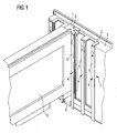
- FIG. 1 shows a slot field 7 in a computer housing 2 and a PCI plug-in card 10 attached to a slot bracket 1 is.
- the slot angle 1 has a vertical section 9 and a horizontal section 8.
- an EMC seal 3 is arranged on the support surface is both for the vertical section 9 of the slot angle 1 as well as for the horizontal section 8 .
- the guide rails 4 are only for the vertical sections 9 of the slot angle 1 is formed.
- Figures 3 and 4 show what effect is achieved when in the guide rail 4 a slot bracket 1 with its vertical Section 9 is inserted.
- Figure 4 shows the view of Figure 3, here two Slot bracket 1 pushed right and left into the guide rail 4 are. Of the slot angles 1, only the vertical ones are Sections 9 shown.
- the invention is not based on the illustrated embodiment limited.
- the EMC seal 3 can also be on the front between slot bracket and guide rail, between slot bracket and aperture 5 or U-shaped in the guide rail his.
- Metal mesh (gasket) or spring plate can be used as EMC seal 3 be used.
Landscapes
- Engineering & Computer Science (AREA)
- Theoretical Computer Science (AREA)
- General Engineering & Computer Science (AREA)
- Computer Hardware Design (AREA)
- Physics & Mathematics (AREA)
- General Physics & Mathematics (AREA)
- Human Computer Interaction (AREA)
- Power Engineering (AREA)
- Microelectronics & Electronic Packaging (AREA)
- Electromagnetism (AREA)
- Shielding Devices Or Components To Electric Or Magnetic Fields (AREA)
- Casings For Electric Apparatus (AREA)
- Coupling Device And Connection With Printed Circuit (AREA)
Abstract
Description
- Figur 1
- eine Schrägansicht eines Slotfeldes mit eingesteckter PCI-Steckkarte und Slotwinkel,
- Figur 2
- eine Draufsicht des Slotfeldes mit eingesteckter PCI-Karte und Slotwinkel,
- Figur 3
- einen Querschnitt durch eine Führungsschiene an einem Slotfeld mit eingesetzter EMV-Dichtung,
- Figur 4
- einen Querschnitt durch eine Führungsschiene am Slotfeld mit eingesetzter EMV-Dichtung und eingeschobenem Slotwinkel.
- 1
- Slotwinkel
- 2
- Computergehäuse
- 3
- EMV-Dichtung
- 4
- Führungsschiene
- 5
- Blende
- 6
- Träger
- 7
- Slotfeld
- 8
- waagrechter Abschnitt
- 9
- senkrechter Abschnitt
- 10
- PCI-Steckkarte
Claims (8)
- Anordnung zur Kontaktierung eines Slotwinkels (1) an einem Slotfeld (7) in einem Computergehäuse (2)
dadurch gekennzeichnet, dass an dem Slotfeld (7) eine Führungsschiene (4) zum Einschieben des Slotwinkels (1) ausgebildet ist. - Anordnung nach Anspruch 1
dadurch gekennzeichnet, dass pro Slotwinkel (1) zwei Führungsschienen (4) ausgebildet sind. - Anordnung nach Anspruch 1 und 2
dadurch gekennzeichnet, dass die Führungsschienen (4) aus zum Slotfeld (7) senkrecht stehenden Trägern (6) und zum Slotfeld (7) parallelen Blenden (5) gebildet sind. - Anordnung nach Anspruch 1 bis 3
dadurch gekennzeichnet, dass zwischen Slotwinkel (1) und Slotfeld (7) eine EMV-Dichtung (3) angeordnet ist. - Anordnung nach Anspruch 1 bis 4
dadurch gekennzeichnet, dass die EMV-Dichtung (3) in den Führungsschienen angeordnet ist. - Anordnung nach Anspruch 1 bis 5
dadurch gekennzeichnet, dass die EMV-Dichtung (3) aus einem komprimierbaren Material besteht. - Anordnung nach Anspruch 1 bis 6
dadurch gekennzeichnet, dass die Dicke der nicht komprimierten EMV-Dichtung (3) zusammen mit der Dicke eines senkrechten Abschnittes (9) des Slotwinkels (1) grösser ist als die lichte Breite der Führungsschiene. - Anordnung nach Anspruch 1 bis 7
dadurch gekennzeichnet, dass bei eingeschobenem Slotwinkel (1) die EMV-Dichtung (3) zusammengepresst ist und mit der entstehenden Gegenkraft der Slotwinkel (1) festgelegt wird.
Applications Claiming Priority (2)
| Application Number | Priority Date | Filing Date | Title |
|---|---|---|---|
| DE10210710A DE10210710B4 (de) | 2002-03-12 | 2002-03-12 | Anordnung zur Kontaktierung eines Slotwinkels |
| DE10210710 | 2002-03-12 |
Publications (3)
| Publication Number | Publication Date |
|---|---|
| EP1347358A2 true EP1347358A2 (de) | 2003-09-24 |
| EP1347358A3 EP1347358A3 (de) | 2005-12-14 |
| EP1347358B1 EP1347358B1 (de) | 2011-04-06 |
Family
ID=27771184
Family Applications (1)
| Application Number | Title | Priority Date | Filing Date |
|---|---|---|---|
| EP03004165A Expired - Lifetime EP1347358B1 (de) | 2002-03-12 | 2003-02-26 | Anordnung zur Kontaktierung eines Einschubwinkels |
Country Status (3)
| Country | Link |
|---|---|
| US (1) | US6965073B2 (de) |
| EP (1) | EP1347358B1 (de) |
| DE (2) | DE10210710B4 (de) |
Families Citing this family (3)
| Publication number | Priority date | Publication date | Assignee | Title |
|---|---|---|---|---|
| DE102006048644B3 (de) * | 2006-10-13 | 2007-11-08 | Siemens Ag | Slotfeld für einen Rechner |
| DE102006053533B3 (de) * | 2006-11-08 | 2008-04-24 | Schäfer Gehäusesysteme GmbH | Chassis für Computergehäuse |
| DE102011014300B3 (de) * | 2011-03-17 | 2012-08-30 | Fujitsu Technology Solutions Intellectual Property Gmbh | Anordnung zum Festlegen eines Slotwinkels |
Citations (4)
| Publication number | Priority date | Publication date | Assignee | Title |
|---|---|---|---|---|
| US5929376A (en) | 1997-06-20 | 1999-07-27 | Tektronix, Inc. | Electromagnetic interference shield and method of manufacturing |
| US6018464A (en) | 1997-03-10 | 2000-01-25 | Samsung Electronics Co., Ltd. | Option card-equipping device for improving electromagnetic shielding and a computer using the same |
| DE10008282A1 (de) | 2000-02-23 | 2001-09-06 | Fujitsu Siemens Computers Gmbh | EMV-Kontaktierung |
| US6349042B1 (en) | 2000-03-24 | 2002-02-19 | Dell Products L.P. | Apparatus for shielding electromagnetic emissions |
Family Cites Families (8)
| Publication number | Priority date | Publication date | Assignee | Title |
|---|---|---|---|---|
| US4873395A (en) * | 1988-11-14 | 1989-10-10 | Compuadd Corporation | Personal computer expansion slot seal and method |
| US4924355A (en) * | 1989-04-25 | 1990-05-08 | Dell Corporate Services Corporation | Personal computer having expansion card adapter bracket |
| DE29510599U1 (de) * | 1995-06-29 | 1995-11-16 | Siemens Nixdorf Informationssysteme AG, 33106 Paderborn | Abdeckvorrichtung für durch Öffnungen in einer Gehäusewandung eines Datenverarbeitungsgerätes zugängliche Einbauplätze für dort einsetzbare Standard-Flachbaugruppen |
| US5748453A (en) * | 1996-07-01 | 1998-05-05 | Sun Microsystems, Inc. | PCI expansion card slide-type retainer |
| US5975953A (en) * | 1997-08-29 | 1999-11-02 | Hewlett-Packard Company | EMI by-pass gasket for shielded connectors |
| US6058025A (en) * | 1998-04-21 | 2000-05-02 | International Business Machines Corporation | Computer tailgate having expansion slot alignment pins |
| DE19948092B4 (de) * | 1999-10-06 | 2006-01-26 | Fujitsu Siemens Computers Gmbh | PC mit EMV-Kontaktierung zwischen Gehäuse und Steckeranschlussfeld |
| DE10048101A1 (de) * | 2000-09-28 | 2002-04-18 | Hermann Stahl Gmbh | Computergehäuse |
-
2002
- 2002-03-12 DE DE10210710A patent/DE10210710B4/de not_active Expired - Fee Related
-
2003
- 2003-02-26 DE DE50313594T patent/DE50313594D1/de not_active Expired - Lifetime
- 2003-02-26 EP EP03004165A patent/EP1347358B1/de not_active Expired - Lifetime
- 2003-03-12 US US10/386,963 patent/US6965073B2/en not_active Expired - Fee Related
Patent Citations (4)
| Publication number | Priority date | Publication date | Assignee | Title |
|---|---|---|---|---|
| US6018464A (en) | 1997-03-10 | 2000-01-25 | Samsung Electronics Co., Ltd. | Option card-equipping device for improving electromagnetic shielding and a computer using the same |
| US5929376A (en) | 1997-06-20 | 1999-07-27 | Tektronix, Inc. | Electromagnetic interference shield and method of manufacturing |
| DE10008282A1 (de) | 2000-02-23 | 2001-09-06 | Fujitsu Siemens Computers Gmbh | EMV-Kontaktierung |
| US6349042B1 (en) | 2000-03-24 | 2002-02-19 | Dell Products L.P. | Apparatus for shielding electromagnetic emissions |
Also Published As
| Publication number | Publication date |
|---|---|
| DE10210710B4 (de) | 2006-09-14 |
| US6965073B2 (en) | 2005-11-15 |
| DE10210710A1 (de) | 2003-10-09 |
| US20030174485A1 (en) | 2003-09-18 |
| DE50313594D1 (de) | 2011-05-19 |
| EP1347358A3 (de) | 2005-12-14 |
| EP1347358B1 (de) | 2011-04-06 |
Similar Documents
| Publication | Publication Date | Title |
|---|---|---|
| EP0754936A2 (de) | Kraftmesseinrichtung | |
| DE10213526A1 (de) | Festlegung einer Einschubbaugruppe in einem Einbaukäfig eines Computers | |
| DE202007009358U1 (de) | Haltekonstruktion für einen Datenspeicher | |
| DE2024390A1 (de) | Abdeckvorrichtung für eine Projektionsanordnung | |
| DE202004000179U1 (de) | Kontaktiereinheit für ein kartenförmiges Trägerelement elektronischer Baugruppen | |
| DE10210710B4 (de) | Anordnung zur Kontaktierung eines Slotwinkels | |
| EP0315707A1 (de) | Adapter für eine Vorrichtung zur elektronischen Prüfung von Leiterplatten | |
| EP0313131A2 (de) | Aufnahmevorrichtung mit geschirmten Leiterplatten | |
| DE102007040085B3 (de) | Computer und Verfahren zur Montage einer Leiterplatte an einem Trägerblech | |
| DE29619565U1 (de) | Baugruppenträger für Leiterplatten mit abgeschirmter Front- und Rückseite | |
| DE202004018857U1 (de) | Blechgehäuse | |
| DE10318524A1 (de) | Elektrischer Verbinder mit einer Anschlagfläche für eine Kontaktfeder | |
| DE2452251B2 (de) | Ausstellvorrichtung | |
| DE102009058181A1 (de) | Träger für Leiterplatte | |
| DE202004010560U1 (de) | Paneel-Verbindungs-Vorrichtung zum Herstellen einer Transportkiste | |
| DE102009048461B3 (de) | Motorantrieb mit einer Einrichtung zur sicheren Montage mit einem Leistungsschalter | |
| DE202008016269U1 (de) | Vorrichtung mit einem Induktorträger zum Tragen und Abschirmen wenigstens eines Induktors in einem Induktionskochfeld | |
| DE1248766B (de) | ||
| DE102006048644B3 (de) | Slotfeld für einen Rechner | |
| DE10113688A1 (de) | Gehäuse, insbesondere für einen Computer | |
| DE10200054C2 (de) | Computergehäuse | |
| DE10108050C1 (de) | Prüfanordnung für elektronische Baugruppen | |
| DE2848212C2 (de) | Planungstafel | |
| DE29907171U1 (de) | Fahrtschreiber mit einem flachen, quaderförmigen Einbaugehäuse und einer quer zur Hochachse des Einbaugehäuses bewegbaren Druckvorrichtung | |
| DE102016225526A1 (de) | Gehäuse für elektrische Bauelemente und Verfahren zum Verbinden eines Gehäusekörpers mit einer Gehäuseabdeckung |
Legal Events
| Date | Code | Title | Description |
|---|---|---|---|
| PUAI | Public reference made under article 153(3) epc to a published international application that has entered the european phase |
Free format text: ORIGINAL CODE: 0009012 |
|
| AK | Designated contracting states |
Kind code of ref document: A2 Designated state(s): AT BE BG CH CY CZ DE DK EE ES FI FR GB GR HU IE IT LI LU MC NL PT SE SI SK TR |
|
| AX | Request for extension of the european patent |
Extension state: AL LT LV MK RO |
|
| RAP1 | Party data changed (applicant data changed or rights of an application transferred) |
Owner name: FUJITSU SIEMENS COMPUTERS GMBH |
|
| PUAL | Search report despatched |
Free format text: ORIGINAL CODE: 0009013 |
|
| AK | Designated contracting states |
Kind code of ref document: A3 Designated state(s): AT BE BG CH CY CZ DE DK EE ES FI FR GB GR HU IE IT LI LU MC NL PT SE SI SK TR |
|
| AX | Request for extension of the european patent |
Extension state: AL LT LV MK RO |
|
| 17P | Request for examination filed |
Effective date: 20060301 |
|
| AKX | Designation fees paid |
Designated state(s): DE FR GB NL |
|
| GRAP | Despatch of communication of intention to grant a patent |
Free format text: ORIGINAL CODE: EPIDOSNIGR1 |
|
| GRAS | Grant fee paid |
Free format text: ORIGINAL CODE: EPIDOSNIGR3 |
|
| GRAA | (expected) grant |
Free format text: ORIGINAL CODE: 0009210 |
|
| AK | Designated contracting states |
Kind code of ref document: B1 Designated state(s): DE FR GB NL |
|
| REG | Reference to a national code |
Ref country code: GB Ref legal event code: FG4D Free format text: NOT ENGLISH |
|
| REF | Corresponds to: |
Ref document number: 50313594 Country of ref document: DE Date of ref document: 20110519 Kind code of ref document: P |
|
| REG | Reference to a national code |
Ref country code: DE Ref legal event code: R096 Ref document number: 50313594 Country of ref document: DE Effective date: 20110519 |
|
| REG | Reference to a national code |
Ref country code: NL Ref legal event code: VDEP Effective date: 20110406 |
|
| PG25 | Lapsed in a contracting state [announced via postgrant information from national office to epo] |
Ref country code: NL Free format text: LAPSE BECAUSE OF FAILURE TO SUBMIT A TRANSLATION OF THE DESCRIPTION OR TO PAY THE FEE WITHIN THE PRESCRIBED TIME-LIMIT Effective date: 20110406 |
|
| PLBE | No opposition filed within time limit |
Free format text: ORIGINAL CODE: 0009261 |
|
| STAA | Information on the status of an ep patent application or granted ep patent |
Free format text: STATUS: NO OPPOSITION FILED WITHIN TIME LIMIT |
|
| 26N | No opposition filed |
Effective date: 20120110 |
|
| REG | Reference to a national code |
Ref country code: DE Ref legal event code: R097 Ref document number: 50313594 Country of ref document: DE Effective date: 20120110 |
|
| REG | Reference to a national code |
Ref country code: DE Ref legal event code: R084 Ref document number: 50313594 Country of ref document: DE Effective date: 20130227 |
|
| REG | Reference to a national code |
Ref country code: FR Ref legal event code: PLFP Year of fee payment: 14 |
|
| PGFP | Annual fee paid to national office [announced via postgrant information from national office to epo] |
Ref country code: DE Payment date: 20160222 Year of fee payment: 14 |
|
| PGFP | Annual fee paid to national office [announced via postgrant information from national office to epo] |
Ref country code: GB Payment date: 20160222 Year of fee payment: 14 Ref country code: FR Payment date: 20160222 Year of fee payment: 14 |
|
| REG | Reference to a national code |
Ref country code: DE Ref legal event code: R119 Ref document number: 50313594 Country of ref document: DE |
|
| GBPC | Gb: european patent ceased through non-payment of renewal fee |
Effective date: 20170226 |
|
| REG | Reference to a national code |
Ref country code: FR Ref legal event code: ST Effective date: 20171031 |
|
| PG25 | Lapsed in a contracting state [announced via postgrant information from national office to epo] |
Ref country code: DE Free format text: LAPSE BECAUSE OF NON-PAYMENT OF DUE FEES Effective date: 20170901 Ref country code: FR Free format text: LAPSE BECAUSE OF NON-PAYMENT OF DUE FEES Effective date: 20170228 |
|
| PG25 | Lapsed in a contracting state [announced via postgrant information from national office to epo] |
Ref country code: GB Free format text: LAPSE BECAUSE OF NON-PAYMENT OF DUE FEES Effective date: 20170226 |