EP1346469B1 - Dreiklasse-e-doherty-verstärkertopologie für signaltransmitter von hoher leistung - Google Patents
Dreiklasse-e-doherty-verstärkertopologie für signaltransmitter von hoher leistung Download PDFInfo
- Publication number
- EP1346469B1 EP1346469B1 EP01990245A EP01990245A EP1346469B1 EP 1346469 B1 EP1346469 B1 EP 1346469B1 EP 01990245 A EP01990245 A EP 01990245A EP 01990245 A EP01990245 A EP 01990245A EP 1346469 B1 EP1346469 B1 EP 1346469B1
- Authority
- EP
- European Patent Office
- Prior art keywords
- amplifier
- amplifiers
- class
- peaking
- output
- Prior art date
- Legal status (The legal status is an assumption and is not a legal conclusion. Google has not performed a legal analysis and makes no representation as to the accuracy of the status listed.)
- Expired - Lifetime
Links
- 238000000034 method Methods 0.000 claims abstract description 15
- 238000004891 communication Methods 0.000 claims description 10
- 230000003321 amplification Effects 0.000 abstract description 5
- 238000003199 nucleic acid amplification method Methods 0.000 abstract description 5
- 238000010586 diagram Methods 0.000 description 11
- 230000005540 biological transmission Effects 0.000 description 10
- 229920006395 saturated elastomer Polymers 0.000 description 10
- 230000007423 decrease Effects 0.000 description 5
- 238000013461 design Methods 0.000 description 4
- 239000003989 dielectric material Substances 0.000 description 4
- 238000013459 approach Methods 0.000 description 3
- 230000008901 benefit Effects 0.000 description 3
- 230000008859 change Effects 0.000 description 3
- 238000001914 filtration Methods 0.000 description 3
- 238000012546 transfer Methods 0.000 description 3
- 230000015556 catabolic process Effects 0.000 description 2
- 238000006731 degradation reaction Methods 0.000 description 2
- 230000000694 effects Effects 0.000 description 2
- 238000005516 engineering process Methods 0.000 description 2
- 238000002955 isolation Methods 0.000 description 2
- 239000000463 material Substances 0.000 description 2
- 238000012986 modification Methods 0.000 description 2
- 230000004048 modification Effects 0.000 description 2
- 230000004044 response Effects 0.000 description 2
- 238000004088 simulation Methods 0.000 description 2
- 238000004513 sizing Methods 0.000 description 2
- 241000282326 Felis catus Species 0.000 description 1
- 238000006243 chemical reaction Methods 0.000 description 1
- 230000007774 longterm Effects 0.000 description 1
- 230000000116 mitigating effect Effects 0.000 description 1
- 238000005457 optimization Methods 0.000 description 1
- 230000003071 parasitic effect Effects 0.000 description 1
- 230000035699 permeability Effects 0.000 description 1
- 230000001105 regulatory effect Effects 0.000 description 1
- 238000000926 separation method Methods 0.000 description 1
- 238000006467 substitution reaction Methods 0.000 description 1
- 230000001629 suppression Effects 0.000 description 1
- 230000009466 transformation Effects 0.000 description 1
- 230000007704 transition Effects 0.000 description 1
Images


Classifications
-
- H—ELECTRICITY
- H03—ELECTRONIC CIRCUITRY
- H03F—AMPLIFIERS
- H03F1/00—Details of amplifiers with only discharge tubes, only semiconductor devices or only unspecified devices as amplifying elements
- H03F1/02—Modifications of amplifiers to raise the efficiency, e.g. gliding Class A stages, use of an auxiliary oscillation
- H03F1/0205—Modifications of amplifiers to raise the efficiency, e.g. gliding Class A stages, use of an auxiliary oscillation in transistor amplifiers
- H03F1/0288—Modifications of amplifiers to raise the efficiency, e.g. gliding Class A stages, use of an auxiliary oscillation in transistor amplifiers using a main and one or several auxiliary peaking amplifiers whereby the load is connected to the main amplifier using an impedance inverter, e.g. Doherty amplifiers
-
- H—ELECTRICITY
- H03—ELECTRONIC CIRCUITRY
- H03F—AMPLIFIERS
- H03F3/00—Amplifiers with only discharge tubes or only semiconductor devices as amplifying elements
- H03F3/20—Power amplifiers, e.g. Class B amplifiers, Class C amplifiers
- H03F3/21—Power amplifiers, e.g. Class B amplifiers, Class C amplifiers with semiconductor devices only
- H03F3/217—Class D power amplifiers; Switching amplifiers
- H03F3/2176—Class E amplifiers
-
- H—ELECTRICITY
- H03—ELECTRONIC CIRCUITRY
- H03F—AMPLIFIERS
- H03F2200/00—Indexing scheme relating to amplifiers
- H03F2200/391—Indexing scheme relating to amplifiers the output circuit of an amplifying stage comprising an LC-network
Definitions
- the present invention relates to power amplifiers.
- the present invention relates to efficient amplification of signals at a non-peaked average power level whose envelope is amplitude modulated, and specifically the application of linear amplification at RF frequencies of such signals up to high power levels.
- the requirements for higher data rates and bandwidth efficiency in wireless communication standards has caused designers to implement varying envelope modulation formats.
- the varying AM content of these formats allows for additional information to be transmitted in a given bandwidth.
- This varying envelope significantly constrains the ability of the power amplifier in a wireless device to linearly transmit the waveform.
- the varying envelope exhibits a "peak-to-average" ratio, where the average envelope power may be significantly below the peak envelope power.
- the power amplifier would be capable of delivering peak power while operating at a much lower average power. Attempts at this, however, typically result in the application "backing-off" the power amplifier from peak in order to avoid clipping and distortion of the output waveform. This also results in an associated large decrease in efficiency from the peak.
- the linearity of the power amplifier often requires that its output power be backed off even further than P SAT ((dBm) - PeakToAvgRatio(dB)) in order to satisfy further constraints in adjacent channel power rejection (ACPR) and error vector magnitude (EVM).
- ACPR adjacent channel power rejection
- EVM error vector magnitude
- the power amplifier must provide "headroom" for the output power to actually reach the peak output power and not saturate prematurely. It thus becomes critical for efficiency that the power amplifier topology be able to maintain efficiency at higher power levels.
- the Doherty arrangement 2 utilizes two power amplifiers 4, 6 that saturate at different input power levels. This allows one amplifier to reach saturation and peak efficiency before the second. Because power amplifiers with higher output load impedances saturate at lower output power levels, the dynamic loading of the first power amplifier by a second amplifier can change the output power level at which it saturates and achieves peak efficiency. This characteristic allows it to behave in a saturated mode over a range of output power because its load impedance decreases along with increasing output power. This dynamic loading and the variation in output impedance over a range of output powers are achieved with a special power-combining load network 8.
- this output power combiner 8 utilizes a quarter-wave transformer 10 with characteristic impedance of 35.36 Ohms to transform from the load resistance of 50 to 25 at the output combiner node 8.
- a second quarter-wave transformer 12 with characteristic impedance of 50 Ohms transforms the output combiner node impedance to the impedance seen at the output of the carrier power amplifier 4.
- a quarter-wave transmission line 14 is inserted at the input of the peaking amplifier 6, so that they sum coherently at their outputs.
- the higher impedance presented to the carrier power amplifier 4 forces it to saturate earlier to optimum load impedance.
- the 2*R OPT load forces it to saturate 3dB below peak.
- a power divider divides an input signal for distribution in three amplifier networks for selective amplification based upon input signal levels. Each amplifier network is biased to respond when the efficiency of the previous stage diminishes. Successive staging of amplifier networks broadens the efficiency bandwidth of power amplifier.
- a combiner merges output signals from each successive amplifier networks to provide an improved efficiency output to a power amplifier load.
- WO 0048307 provides for power control of a high-efficiency (e.g., hard-limiting or switch-mode) power amplifier in such a manner as to achieve a desired modulation.
- the amplitude modulation of the output signal is achieved by providing a regulated power amplifier operating voltage that causes the amplifier to reproduce the desired amplitude modulation waveform.
- an arrangement comprising a number of separate switch-mode power amplifier connected in parallel for providing higher effects.
- the proposed invention introduces a novel extension of the Doherty concept to more than two stages, thereby extending the output power range over which peak efficiency may be attained.
- the general application of these architectures is further described with the use of class E amplifying stages with their significantly higher efficiencies.
- chips E amplifiers are utilized, and input modulation approaches proposed by the Inventor are Implemented. These implementations are disclosed in Case Reference Nos. P10550-US1-BMOT, P10551-US1-BMOT, and P10552-US1-BMOT, filed concurrently herewith.
- a first embodiment of an amplifier circuit comprising at least three class E amplifiers receiving separated amplitude and phase information from at least one signal source, at least one first impedance adjustment device linked between the signal source and the inputs to at least two of the amplifiers, and a plurality of second impedance adjustment devices linked to the outputs of the amplifiers to combine the outputs Into an output of the circuit.
- the amplifier circuit according to the invention further comprises a control device in connection with at least one of the amplifiers, which control device is adapted for receiving amplitude information and/or phase information from a primary waveform.
- a plurality of switching devices are arranged in communication with the control device and the at least one amplifier.
- the control device is configured to use the information to select an active switching device to create a secondary waveform for input to the matching network of the at least one amplifier.
- another embodiment of a amplifier' circuit comprising at least one signal source producing a plurality of digital amplitude modulation signals and a digital phase modulated signal, and a first class E carrier amplifier linked to receive one of the amplitude modulation signals and the phase modulation signal.
- a first class E peaking amplifier is linked to receive another of the amplitude modulation signals and the phase modulation signal via one or more impedance adjusting devices.
- a second class E peaking amplifier is linked to receive another of the amplitude modulation signals and tho phase modulation signal via one or more impedance adjusting devices.
- a combining circuit links the outputs of the amplifiers via one or more impedance adjusting devices.
- the invention may also be embodied in a method of providing high-efficiency signal amplification.
- the method comprises the steps of providing a first digital amplitude waveform to a class E carrier amplifier, providing a first digital phase waveform to a first class E peaking amplifier, providing a second digital phase waveform to a second class E peaking amplifier, providing a shared digital phase waveform to the carrier and peaking amplifiers, and combining the outputs of the carrier and peaking amplifiers via one or more impedance adjusting devices to produce an amplified signal output.
- the various amplifier embodiments referred to above and disclosed herein involve the use of saturated class E amplifiers.
- the input to the amplifiers is modulated in various ways to vary the output power.
- Each of these approaches may be utilized here, but the TIMER input modulation scheme ( T ransmitter using I nput M odulation for E nvelope R estoration) is used as an example throughout the preferred embodiment herein for purposes of continuity.
- the use of the TIMER scheme in the present embodiment involves utilizing a dual-gate FET device as the active switch component in a class E design as shown in FIG. 2. Generally, one switch is driven by the phase-only constant envelope information, and the other switch is used to modulate the output power envelope.
- the use of this second envelope terminal allows for the power amplifier to be turned ON independently of the drive level, affording more flexibility for Doherty-like schemes where the peaking amplifier is typically turned on based on the input drive power level.
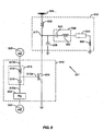
- FIG. 2 is a diagram of an active device switching circuit 210 combined with an output load matching network 212 to make up a class E amplifier 201.
- the circuit 210 preferably includes a pair of switching devices 214 and 216, each of which may be independently controlled to exhibit different resistances to the total current flowing through the pair.
- the switching devices should be lower minimum "ON" resistance devices with high-speed switching capabilities, one example would be the MwT-5 Dual-gate FET (reference http://www.mwtinc.com/cat/fets/htm/new-html/MwT-5_1.htm) manufactured by MwT, Inc. These devices are exemplary only for this embodiment, and a wide variety of other components or structures may be substituted for the components described in accordance with the knowledge of one skilled in the art.
- the switching devices 214, 216 are linked in series or "cascode" as shown connected to the output load matching network 212 at node 217.
- the gates 214a and 216a of each of the transistors 214 and 216 receive phase information 224 and amplitude information 226, respectively, from a primary waveform.
- the received information 224 and 226 into the gates 214a and 216a of the transistors 214 and 216 is utilized to vary the switching resistance of the transistors in accordance with the input primary waveform to create a secondary waveform at node 217.
- the implemented standard class E amplifier comprises a single transistor switch and an output load matching network 212.
- the connection node 217 between the active switch devices 210 and this standard class E output load matching network 212 comprises an inductance coil 232 connecting to the supply voltage Vdd 234.
- a capacitance 236 which includes parasitic capacitance from the active device(s) in parallel with the active device output impedance.
- a tuned circuit filter 238 consisting of a capacitance 240 and an inductance 242 is connected in series with a reactive component 244 and a load resistance 246, nominally 50 Ohms.
- frequency and phase modulation information is received from the switches at node 217, and amplitude modulation information is received by variation of the supply voltage Vdd at 234.
- phase and amplitude information 224 and 226 are both received as a switched input at 214a and 216a and the input terminals are used to combine phase and amplitude information to a desired signal at node 217, such that the final signal delivered to the load 246 is as desired.
- a matching network 220 is linked to input gate 214a of the active switching device 214 to provide optimum power transfer from the phase modulated source to the switching device 214.
- the matching network 220 may comprise a number of reactive elements according to known methods.
- Another matching network 221 is linked to the input gate 216b of the active switching device 216 to block any phase information from reaching the amplitude modulated source, while still providing a low frequency path from the amplitude modulated source to the switching device 216.
- This second matching network also may comprise a combination of reactive elements according to known methods.
- the active switching device 214 is gated on and off through the gate 214a in accordance with the received phase information 224.
- the switching device 216 is gated on and off via the input 216a in accordance with envelope information 226 received at the gate.
- envelope information 226 received at the gate.
- switch 216 can thus be driven with a low frequency signal so that the "ON" resistance of the switch 216 produces a flexibly adjusted output amplitude and thus restores the output envelope amplitude.
- the second switch 216 is continuously variable and allows for a smoothly continuous change in the "ON" resistance, and an associated continuous change in the output envelope amplitude.
- the switching device 216 slowly varies the envelope information.
- the function of this information in the switch configuration of the circuit 210 is to provide additional isolation of the RF feedthrough between the high-speed switching of the phase information input and the node connected to the load network.
- the switching device 214 receives a high-frequency input and has a direct source connection to the load-inductance ground for enhanced stability.
- the node 215 between the switches 214 and 216 traces the output node connected to the load network, thereby causing the switch 216 to switch on and off at the same frequency as the lower switch.
- the switching device 214 receives a high-frequency input and has a direct source connection to low inductance ground for enhanced stability.
- the switches are capable of switching at high frequencies so that maximum gain and efficiency may be attained from this cascode configuration.
- the present switching circuit 210 advantageously allows a single RF input into the matching network 212 and a second low-frequency baseband envelope input to achieve the variable "ON" resistance necessary for input into the matching network 212. This reduces the necessity for multiple RF inputs and associated high-frequency signal lines on valuable circuit board real estate. Furthermore, the requirement for multiple matching networks or multiplexing functions preceding the actual matching network 212 are not required.
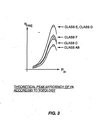
- the peak efficiency is much higher than the class C configuration, theoretically 100% vs. 85% (for 73.5° conduction angle in class C case) as diagrammed in FIG. 3.
- Realistically achievable efficiencies at RF frequencies for class E vs. class C devices are upwards of 80% vs. 65% respectively.
- One shortcoming of the TIMER scheme is that for modulation formats requiring envelope variation, the average efficiency falls off as a function of the output power back off required. In simulation environments, a 3dB peak-to-average ratio results in a peak efficiency of greater than 80%, but average efficiency at roughly 50%. This roll-off in efficiency results because of the loss inherent in the increased switching ON resistance of the active device that is the basis for the modulation of the output envelope.
- FIG 4. A first implementation of an embodiment of a Doherty scheme using the TIMER input modulation of class E amplifiers is shown in FIG 4.
- the two amplifiers 404, 406 shown in this embodiment are both driven by a phase-only constant envelope signal, and the separate envelope modulation inputs are used to stagger the output powers of the carrier and peaking amplifiers to result in an extended peak efficiency range.
- the carrier amplifier reaches saturation at peak power and efficiency with the peaking amplifier off, the peaking amplifier is turned on and the efficiency range is extended to the point where both amplifiers deliver their peak output powers equally, and the maximum combined output power is reached.
- the Doherty concept is extended in an attempt to increase the range of the peak efficiency to beyond 6dB backed-off from peak. This is accomplished by using more than just the two stages shown in FIG. 4.
- a three-stage Doherty configuration is shown in the amplifier circuit 501 of FIG. 5 and represents an extension of the peak efficiency to as much as 9.5dB backed-off from peak.
- three linked class E amplifiers 504, 506, and 508 are arranged as shown in the schematic diagram.
- the amplifier 504 acts as the carrier amplifier, while the amplifiers 506 and 508 act as the first and second peaking amplifiers, respectively.
- the outputs 504a, 506a, and 508a are linked by quarter-wave lines 510 and 512 having characteristic impedances of 50ohms and 17.68ohms, respectively.
- the outputs of the amplifiers are linked at 514a to a 25ohm quarter-wave line 514.
- the quarter-wave line 514 is in turn linked to the RF output 518 and a load resistance 516.
- the digital signal processor 500 generates the separated amplitude and phase waveforms via outputs 540, 542, 543 and 544, completely controls the delay that is introduced between the phase and amplitude signal paths.
- the outputs 540, 542 and 546 output an amplitude modulated signal for the carrier and the peaking power amplifiers 504, 506 and 508, respectively.
- High bit-rate digital to analog converters 550, 552 and 556 are connected to the outputs 540, 542 and 546, respectively, to convert the digital signals from the DSP 500 to analog signals before connection to the amplifiers 504, 506 and 508.
- the output 543 of the DSP 500 produces a shared phase-modulated waveform at the RF frequency for input into the amplifiers 504, 506 and 508.
- the output 543 inputs the digital signal from the DSP 500 to a high bit-rate digital to analog converter 554 for conversion of the signal to analog format.
- the converter 554 is in turn linked to a quadrature-modulating upconverter 560 and a bandpass noise filter 562 if required.
- a filter is not required for the baseband amplitude modulated signals.
- the output of the bandpass noise filter 562 is input directly into the class E carrier amplifier 504.
- the phase modulation signal provided at line 520 is impedance-corrected by 50 ohm quarter-wave lines at the inputs of the first and the second peaking amplifiers 506 and 508.
- the quarter-wave line 522 is linked to the input to the amplifier 506, and a pair of quarter-wave lines 524a and 524b are series-linked to an input of the peaking amplifier 508.
- One advantage of the architecture of FIG. 5 is that only a single filter for the shared phase modulated RF signal is required for suppression of out-of-band noise, as the amplitude modulated baseband signals do not require filtering.
- the digital signal processor (DSP) is used to generate all three required signals, and high bit-rate digital-to-analog converters (DAC) are used to output high-resolution analog signals for the power amplifier inputs.
- the bandpass filtering of the RF frequency phase modulated input signal may or may not be required in this implementation depending on the architecture of the modulator block and the specific communication standard applied.
- the principle in the circuit 501 is similar to the basic Doherty, with the following sequence of amplifier behavior and corresponding output impedances presented to each amplifier 504, 506 and 508 by the load network of quarter-wave transmission lines: Amplifier Sequence Carrier Amplifier State / Rout Peaking Amplifier #1 State / Rout Peaking Amplifier #2 State / Rout Total Solution Output 1 Saturated/100 Ohms Off/25 Ohms Off/12.5 Ohms 9dB 2 Saturated/50 Ohms Saturated/50 Ohms Off/12.5 Ohms 3dB below 3 Saturated/100 Ohms Saturated/25 Ohms Saturated/25 Ohms Peak
- the means for presenting these specific impedances to the amplifier stages is a novel combiner network of the invention where the quarter-wave lines diagrammed in FIG.
- the operation of the three-stage example in FIG. 5 proceeds according to the sequence of the above Table and begins with the lone carrier amplifier 504 powered on and presented with a 100 Ohm load at its output. Because the carrier amplifier of this example is optimized for peak power output at a load impedance of 50 Ohms, it will saturate at an output power 3dB lower than that optimum case. As the first peaking amplifier 506 turns on, the two branches feeding into quarter-wave line 512 (output 506a and the quarter-wave line 510) increase in impedance because two power sources in parallel are feeding that 25 Ohm impedance.
- the impedance presented to the quarter-wave line 510 goes up by a factor of two to 50 Ohms, and the corresponding inverted impedance transformed to the output of carrier amplifier 504 goes down by a factor of two, to 50 Ohms.
- the impedance presented to the first peaking amplifier 506 is 50 Ohms as well, and both amplifiers deliver equal output power combining for roughly 6dB more total output power than in sequence 1 where the carrier amplifier operated alone.
- the impedance presented to both the output of the second peaking amplifier 508 (508a) and the quarter-wave line 512 go up by a factor of two to 25 Ohms.
- the impedances presented to the output of the first peaking amplifier 506 and carrier amplifier 504 become 25 Ohms and 100 Ohms respectively.
- the second peaking amplifier sees a 25 Ohm load at its output also, and the first and second peaking amplifiers deliver equal power at the maximum capable for the total amplifier solution, roughly 3dB above sequence 2 and a full 9dB above sequence 1.
- the sum of the individual amplifier power levels shown in the Table above result in the overall amplifier output power, and peak efficiency is maintained over a range of over 9dB.
- a critical aspect of the selection of these output impedance levels and the corresponding values of the quarter-wave impedance inverting transmission lines is that the output impedance presented to the amplifiers that are OFF and about to ramp up must be greater than the critical low resistance value for which the output power and efficiency all drop off rapidly. If that resistance is too low (12.5 ⁇ in the case of the amplifier 508 in the above table), then the transition as the amplifier 508 starts to contribute will cause a significant dip in the drain efficiency of the overall amplifier circuit 501.
- Simulations for this configuration show that the peak efficiency is maintained at close to 80%.
- the configuration is designed to peak exactly at 3dB below the peak output power of the entire amplifier circuit 501. This is an ideal behavior for signals with a peak-to-average power ratio of 3.2dB such as IS-136 and EDGE.
- the addition of the third amplifier path (peaking amplifier 508) provides for significantly higher efficiency down to greater than 9dB output power back-off, and significantly extends the power range for peak efficiency over the two-path CEDA implementations of two-path Doherty configurations.
- An additional extension of this concept is to size the amplifiers differently and to design the quarter-wave transmission lines differently such that a wider dynamic range is achieved.
- the carrier amplifier By sizing the carrier amplifier to be smaller than the peaking amplifiers, the lowest peak in efficiency will occur at a much lower power level and may be optimized for the specifics of a given communication system. As the ability of the carrier and peaking amplifiers to deliver the same peak power becomes limited by this, the efficiency at power levels between sequences 1 and 2, and 2 and 3 in the Table will become smaller causing larger dips in efficiency at power levels between those at which the amplifiers are delivering equal power. Some mitigation of this can be achieved by optimal sizing of the quarter-wave transmission lines, in order to optimize the power levels for which unequal impedances are presented to the combination of amplifiers.
- An additional extension of the present three-stage embodiment is to add yet another path for a total of four paths.
- This is shown in the schematic, diagram of FIG. 6, wherein a quadruple amplifier circuit is shown including the carrier amplifier 604 and three peaking amplifiers 606, 608 and 609.
- the four amplifiers 604, 606, 608 and 609 define four stages 603, 605 and 607, including the fourth stage 611 as shown.
- the fourth stage 611 includes the third peaking amplifier 609 connected to receive the amplitude modulated signal via the input 609b from a signal-generating source.
- the peaking amplifier 609 also receives the shared phase modulation input through three quarter-wave, 50ohm impedance lines 613, 615 and 617 linked in series as shown.
- the output 604a of the carrier amplifier 604 is linked to the output 606a of the first peaking amplifier 606 via a 100ohm quarter-wave line 618. These outputs are in turn linked to the output 608a of the second peaking amplifier 608 via a 35.35ohm quarter-wave line 614. These outputs are linked, in turn, to the output 609a of the third peaking amplifier 609 via a 17.68ohm quarter-wave line 612.
- the remainder of the circuit 601 is similar to that shown in FIG. 5 above.
- This implementation extends the dynamic range of the peak efficiency further, and additional paths can be implemented until the circuit starts to exceed the reasonable range of characteristic impedance required in the design of the quarter-wave transmission lines, the complexity of predistorting additional envelope terminal voltages, and the area and output losses start to impact performance.
- These limitations depend on the core amplifier design and the transmission line technology implemented. The other implication is that the very high impedance seen by the carrier amplifier when it operates alone will become very high and the class E efficiency will eventually degrade significantly, but still operating at higher efficiencies than an amplifier of fewer paths at that minimum power.
- some amplitude and phase predistortion is required so that the envelope modulation on the input translates to the desired output envelope satisfying linearity specifications of adjacent channel power ratio (ACPR) and error vector magnitude (EVM).
- ACPR adjacent channel power ratio
- EVM error vector magnitude
- FIG. 7 wherein the phase is adjusted so that the AM/PM can be compensated.
- a unique input waveform for any given desired output may be defined so that a baseband digital signal processor can properly generate the corrected input waveform.
- This predistortion methodology is well-known in the art.
- an additional feedback loop may be implemented to periodically update the input-to-output relationship in accordance with any long-term degradation requirements.
- a feedback loop 702 may be used to sense any voltage standing wave ratio ("VSWR") reflection from the antenna 774.
- the feedback loop may then control the digital signal processor 700 to adjust the amplitude information to correct for any VSWR reflection before the amplitude information is received by the amplifiers 704, 706 and 708. With this predistortion in place, the linearity of the amplifier module can be achieved with extremely high efficiency.
- VSWR voltage standing wave ratio
- the peak efficiency is much higher for the class E implementation, allowing the use of extremely high efficiency, constant envelope modulation within the same power amplifier module.
- the use of fixed DC voltage steps down from the battery voltage allows for the same efficiency performance down to extremely low voltages. These voltages are even lower than for standard Doherty implementations using class B or C amplifiers.
- distinctive advantages are possible through the use of class E amplifiers. These amplifiers allow for minimum die dimension and the smallest single stage power amplifier of all classes of amplifiers. The potential for stable use of ultra-small gate dimension FET's is not possible with other amplifier topologies.
- the efficiency at lower output power levels for this configuration is governed by the carrier amplifier alone as the peaking amplifier is turned off. This efficiency will be better than for a single class E amplifier sized for the peak output power, because the carrier amplifier is designed to saturate at roughly 3dB below the peak output power of the triple stage Doherty class E module proposed. This results in a shift of the entire efficiency curve down in power by roughly 3dB and a net higher efficiency at all levels.
- the present invention may also be implemented in alternative configurations. Most importantly, other input modulation schemes may be utilized with implementations of the present invention, either substituted for or used in addition to the TIMER scheme illustrated herein.
- FIG. 8 shows a diagram of a active device switching circuit 810 combined with an output load matching network 812 to make up an amplifier 801.
- the circuit 810 preferably includes a single switching device 816 linked to a tuned filter 815.
- the switching device 816 should be a lower minimum "ON" resistance device with high-speed switching capabilities, one example would be the 2SK2922 LDMOS RF discrete FET transistor manufactured by Hitachi, Inc. (http://www.hitachi.co.jp/Sicd/English/Products/transise.htm). These devices are exemplary only for this embodiment, and a wide variety of other components or structures may be substituted for the components described in accordance with the knowledge of one skilled in the art.
- the filter 815 preferably includes a capacitance 818 and an RF choke coil 819 linked in series and through their central connection node to the gated input 816a to the switching device 816.
- These devices are exemplary only, and a wide variety of other components or structures may be substituted for the components described in accordance with the knowledge of one skilled in the art.
- the filter 815 utilizes the capacitance 818 and the RF choke 819 for summation of the combined DC envelope and RF phase waveforms. Using this preferred configuration to combining the waveforms, the variation in "ON" voltage is small and the "ON" resistance can in turn be controlled with a minimum of distortion.
- the switching device 816 is in turn linked as shown to the load network input 817 of the amplifier 812.
- the gate 816a of the switching device 816 receives a combined input of phase information 824 and amplitude information 826 that are input into the filter 815 through inputs 815a and 815b, respectively, from a primary waveform.
- a matching network 820 is linked to input 815a to provide optimum power transfer from the phase modulated source through the tuned filter to the input gate 816a of the switching device 816.
- the matching network 820 may comprise a number of reactive elements according to known methods.
- the received information 824 and 826 is utilized to vary the switching resistance of the switching device 816 in accordance with the input primary waveform to create a secondary waveform for the amplifier input 817.
- the active switching device 816 is gated on and off through the gate 816a in accordance with the combined received phase and amplitude information 824 and 826. Given that the device 816 switches at an RF frequency between an entirely off state to an entirely on state, the output across the load resistance 846 of the matching network 812 is determined by the modulated "ON" resistance of the switching device 816.
- the switch 816 can thus be driven with a low frequency signal so that the "ON" resistance of the switch 816 produces a flexibly adjusted output amplitude and thus restores the output envelope amplitude.
- the switching device 816 slowly varies the envelope information.
- the function of this information in the switch configuration of the circuit 810 provides additional isolation of the RF feedthrough between the high-speed switching of the phase information input and the node connected to the load network.
- the present switching circuit 810 advantageously allows a single RF input into the matching network 812 and a low-frequency baseband envelope input to achieve the variable "ON" resistance necessary for input into the matching network 812. This reduces the necessity for multiple RF inputs and associated high-frequency signal lines on valuable circuit board real estate. Furthermore, the requirement for multiple matching networks or multiplexing functions preceding the actual matching network 812 are not required.
- FIG. 9 is a diagram of a active device switching circuit 910 combined with an output load matching network 912 to make up an amplifier 901.
- the circuit 910 preferably includes a control device 914 and a plurality of switching devices 916, 918, 920, and 922, each having a different current resistance, and a control device 914.
- the control device is preferably a multiplexer, such as that commonly available from Motorola, Inc.
- the switching devices should be lower minimum "ON" resistance devices with high-speed switching capabilities, one example would be the 2SK2922 LDMOS RF discrete FET transistor manufactured by Hitachi, Inc.
- the control device 914 receives amplitude information 924 and phase information 926 from a primary waveform.
- the phase information 926 and amplitude information 924 are received into inputs 914a and 914b of the control device 914.
- a matching network 928 is linked to input 914b to provide optimum power transfer from the phase modulated source through the control device 914 to input gates 916a, 918a, 920a, and 922a of the switching devices 916, 918, 920, and 922.
- the matching network 928 may comprise a number of reactive elements according to known methods. Alternative embodiments may include and/or replace matching network 928 with individual matching networks following the control device 914 for further optimization of the input matching for these different-sized switching devices 916, 918, 920, and 922.
- the control device 914 uses the amplitude information 924 to select an active switching device from the plurality of switching devices 916, 918, 920, and 922.
- the switching devices 916, 918, 920, and 922 are controlled by the control device 914 via inputs 916a, 918a, 920a, and 922a.
- the control device 914 uses the phase information 926 to control the active switching device to create a secondary waveform for input to the amplifier load network 912 at node 917.
- control device 914 controls the active switching devices in accordance with the phase information 926.
- the control device 914 preferably turns the active switching device off and on in response to the phase information 926.
- the switch voltage varies between zero and the peak switch voltage of the active switching device.
- the control device 914 selects an active switching device in accordance with the amplitude information 924 to achieve a desired peak switch voltage.
- the peak amplitude of the switch voltage may be varied to produce a quantized approximation of the amplitude envelope of the primary waveform.
- the amplitude information 924 and phase information 926 are used to create a secondary waveform that approximates the primary waveform. The secondary waveform is then provided as input to the 912 matching network of the amplifier 901.
- high dielectric materials may be used to shrink the combiner network in the above embodiment.
- the effective electrical length is a function of the relative dielectric permittivity of the material on which the microstrip transmission line is fabricated. The electrical length depends on the inverse square root of ⁇ r . Building the transmission lines for 1 GHz operation on FR4 standard PCB material with a relative dielectric constant of 4 will mean that each quarter wave line will be approximately 1.48 inches in length. This would shrink to approximately 0.33 inches by using a high dielectric material with relative permeability of approximately 80. The use of a hybrid module assembly employing high dielectric material could be implemented to significantly decrease the size of the solution.
- the DC control voltage may be modified to achieve peak efficiency at lower discrete power states.
- An additional aspect of the class E amplifiers used in this scheme is that they retain their efficiency for a given load network better than all other topologies as the DC supply voltage is dropped. This is caused by the variation in output impedance as the supply decreases, and degradation in the output match for the power amplifier.
- the DC supply voltage may be controlled in fixed increments so that the DC level can control the absolute average power level, keeping the phase drive and envelope modulation the same for the input drive.
- the variation in the AM/PM with DC supply voltage will require some phase predistortion, but the efficiency is maintained at peak levels down to very low powers.
Landscapes
- Engineering & Computer Science (AREA)
- Power Engineering (AREA)
- Amplifiers (AREA)
- Microwave Amplifiers (AREA)
Claims (18)
- Verstärkerschaltung, mindestens drei Klasse-E-Verstärker (504, 506, 508, 604, 606, 608, 609, 704, 706, 708) umfassend, konfiguriert zum Empfangen getrennter Amplituden- und Phaseninformation von mindestens einer Signalquelle (500, 700);
mindestens eine Impedanzabstimmeinrichtung (524a, 524b, 613, 615, 617), verbunden zwischen der mindestens einen Signalquelle und den Eingängen zu mindestens zwei Verstärkern; und
eine Vielzahl von zweiten Impedanzabstimmeinrichtungen (510, 512, 514, 612, 614, 618), verbunden an die Ausgänge der Verstärker zum Kombinieren der Ausgangsgrößen in einer Ausgangsgröße der Schaltung, wobei die Verstärkerschaltung gekennzeichnet ist durch:wobei die Steuereinrichtung konfiguriert ist zum Verwenden der Information zum Auswählen einer aktiven Schalteinrichtung zum Erstellen einer sekundären Schwingungsform zur Eingabe in das Anpassungsnetz von dem mindestens einen Verstärker.eine Steuereinrichtung (914) für mindestens einen der zum Empfangen von Amplitudeninformation oder Phaseninformation von einer Primärschwingungsform konfigurierten Verstärker; undeine Vielzahl von aktiven Schalteinrichtungen (916, 918, 920, 922) in Kommunikation mit der Steuereinrichtung (914) und dem mindestens einen Verstärker, wobei die aktiven Schalteinrichtungen jeweils einen unterschiedlichen Stromwiderstand; - Verstärkerschaltung nach Anspruch 1, dadurch gekennzeichnet, dass die Schaltung konfiguriert ist, um es einem der Verstärker zu erlauben in die Sättigung zu gelangen bevor der andere Verstärker in die Sättigung gelangt.
- Verstärkerschaltung nach Anspruch 1 oder 2, dadurch gekennzeichnet, dass die Signalquelle einen Digitalsignalprozessor (500, 700) umfasst, der Ausgangssignale erzeugt.
- Verstärkerschaltung nach Anspruch 3, dadurch gekennzeichnet, dass der Klasse-E-Verstärker ferner einen ersten, einen zweiten und einen dritten Verstärker umfasst, wobei der erste Verstärker als Trägerverstärker funktioniert, konfiguriert zum Empfangen eines ersten Amplituden modulierten Basisbandsignals von dem Digitalsignalprozessor, der zweite und der dritte Verstärker konfiguriert zum Empfangen eines gemeinsamen Amplituden modulierten Basisbandsignals von dem Digitalsignalprozessor.
- Verstärkerschaltung nach einem der Ansprüche 1 bis 4, dadurch gekennzeichnet, dass jeder der Klasse-E-Verstärker konfiguriert ist zum Verwenden eines Hüllkurvensignals zum Abstimmen seines individuellen Ausgangsleistungspegels.
- Verstärkerschaltung nach einem der Ansprüche 1 bis 5, dadurch gekennzeichnet, dass die Impedanzabstimmeinrichtung ferner Viertelwellentransformatorleitungen umfasst.
- Verstärkerschaltung nach einem der Ansprüche 1 bis 6, dadurch gekennzeichnet, dass die aktiven Schalteinrichtungen Transistoren sind, von denen jeder ein Gate hat, und die Steuereinrichtung die aktiven Schalteinrichtungen durch Bereitstellen der Information an dem Gate der Schalteinrichtung steuert.
- Verstärkerschaltung nach einem der Ansprüche 1 bis 7, dadurch gekennzeichnet, dass sie eine Rückkopplungsschleife umfasst zum Erfassen von VSWR-Reflektion von einer in Kommunikation mit den Ausgängen der Verstärker stehenden Antenne, wobei die Rückkopplungsschleife in Kommunikation steht mit dem Digitalsignalprozessor; wobei der Digitalsignalprozessor seine Ausgangssignale anpasst zum Korrigieren in bezug auf die VSWR-Reflektion.
- Verstärkerschaltung nach einem der Ansprüche 1 bis 8, dadurch gekennzeichnet, dass mindestens zwei der Verstärker unterschiedliche Ausgangsleistungen haben.
- Verstärkerschaltung nach einem der Ansprüche 1 bis 9,
dadurch gekennzeichnet, dass
die Signalquelle eine Vielzahl von digitalen Amplitudenmodulationssignalen und ein digitales phasenmoduliertes Signal erzeugt;
einer der Klasse-E-Verstärker ein Klasse-E-Trägerverstärker ist, verbunden zum Empfangen eines der Amplitudenmodulationssignale und des Phasenmodulationssignals;
ein anderer der Klasse-E-Verstärker ein erster Klasse-E-Spitzenwertverstärker ist, verbunden zum Empfangen eines anderen der Amplitudenmodulationssignale, wobei der erste Spitzenwertverstärker ferner das Phasenmodulationssignal über eine oder mehrere Impedanzabstimmeinrichtungen empfängt;
noch ein weiterer der Klasse-E-Verstärker ein zweiter Klasse-E-Spitzenwertverstärker ist, verbunden zum Empfangen eines anderen der Amplitudenmodulationssignale, wobei der zweite Spitzenwertverstärker ferner das Phasenmodulationssignal über eine oder mehrere Impedanzabstimmeinrichtungen empfängt; und
die zweiten Impedanzabstimmeinrichtungen eine Kombinierungsschaltung bildet, die Ausgänge der Verstärker verbindend. - Verstärkerschaltung nach einem der Ansprüche 1 bis 10, dadurch gekennzeichnet, dass sie eine Vorrichtung umfasst zum Modulieren der Eingangsgröße zu mindestens einem der Verstärker.
- Verstärkerschaltung nach einem der Ansprüche 10 bis 11, dadurch gekennzeichnet, dass noch ein weiterer der Klasse-E-Verstärker ein dritter Klasse-E-Spitzenwertverstärker ist, verbunden zum Empfangen eines anderen der Amplitudenmodulationssignale, wobei der dritte Spitzenwertverstärker ferner das Phasenmodulationssignal über eine oder mehrere Impedanzabstimmeinrichtungen empfängt.
- Verstärkerschaltung nach einem der Ansprüche 1 bis 12, dadurch gekennzeichnet, dass sie eine Rückkopplungsschleife umfasst zum Umfassen von VSWR-Reflektion von einer mit dem Verstärker in Kommunikation stehenden Antenne, wobei die Rückkopplungsschleife in Kommunikation steht mit dem Digitalsignalprozessor;
wobei der Digitalsignalprozessor das mindestens eine Ausgangssignal abstimmt zum Korrigieren in bezug auf die VSWR-Reflektion. - Verstärkerschaltung nach einem der Ansprüche 4 bis 13, dadurch gekennzeichnet, dass der Trägerverstärker und der erste Spitzenwertverstärker unterschiedliche Ausgangsleistungen haben.
- Verfahren zum Bereitstellen von hocheffizienter Signalverstärkung, wobei eine erste Digitalamplitudenschwingungsform und eine erste Digitalphasenschwingungsform einem Klasse-E-Trägerverstärker bereitgestellt werden; eine zweite Digitalphasenschwingungsform einem zweiten Klasse-E-Spitzenwertverstärker zur Verfügung gestellt wird; eine gemeinsam Digitalphasenschwingungsform den Träger- und Spitzenwertverstärkern bereitgestellt wird; und die Ausgänge der Träger- und Spitzenwertverstärker über eine oder mehrere Impedanzabstimmeinrichtungen kombiniert werden zum Erzeugen einer verstärkten Signalausgangsgröße, wobei das Verfahren gekennzeichnet ist durch die Schritte:Versehen mindestens eines der Verstärker mit Amplitudeninformation oder Phaseninformation von einer Primärschwingungsform; undSelektieren einer aktiven Schalteinrichtung aus einer Vielzahl aktiver Schalteinrichtungen (916, 918, 920, 922) zum Erstellen einer sekundären Schwingungsform zur Eingabe in das Anpassungsnetz des mindestens einen Verstärkers zur Eingabe in ein Anpassungsnetz des mindestens einen Verstärkers.
- Verfahren nach Anspruch 15, den Schritt des Abstimmens der Impedanz der gemeinsamen Digitalphasenschwingungsform über eine oder mehrere Impedanzabstimmeinrichtungen umfassend vor dem Bereitstellen der Schwingungsform für die Spitzenwertverstärker.
- Verfahren nach Anspruch 15 oder 16, den Schritt des Bereitstellens einer dritten Digitalphasenschwingungsform für einen dritten Klasse-E-Spitzenwertverstärker umfassend.
- Verfahren nach einem der Ansprüche 15 bis 17, die Schritte des Erfassens von VSWR-Reflektion von einer Antenne umfassen, die in Kommunikation steht mit dem Signalausgang; und das Abstimmen mindestens einer der Schwingungsformen vor dem Bereitstellen der Schwingungsform zu den Träger- und Spitzenwertverstärkern zum Korrigieren bezüglich der VSWR-Reflektion.
Applications Claiming Priority (3)
| Application Number | Priority Date | Filing Date | Title |
|---|---|---|---|
| US752178 | 2000-12-29 | ||
| US09/752,178 US6472934B1 (en) | 2000-12-29 | 2000-12-29 | Triple class E Doherty amplifier topology for high efficiency signal transmitters |
| PCT/US2001/049153 WO2002054589A2 (en) | 2000-12-29 | 2001-12-19 | Triple class e doherty amplifier topology for high efficiency signal transmitters |
Publications (2)
| Publication Number | Publication Date |
|---|---|
| EP1346469A2 EP1346469A2 (de) | 2003-09-24 |
| EP1346469B1 true EP1346469B1 (de) | 2005-10-26 |
Family
ID=25025224
Family Applications (1)
| Application Number | Title | Priority Date | Filing Date |
|---|---|---|---|
| EP01990245A Expired - Lifetime EP1346469B1 (de) | 2000-12-29 | 2001-12-19 | Dreiklasse-e-doherty-verstärkertopologie für signaltransmitter von hoher leistung |
Country Status (6)
| Country | Link |
|---|---|
| US (1) | US6472934B1 (de) |
| EP (1) | EP1346469B1 (de) |
| CN (1) | CN1280984C (de) |
| AT (1) | ATE308156T1 (de) |
| DE (1) | DE60114451T2 (de) |
| WO (1) | WO2002054589A2 (de) |
Families Citing this family (97)
| Publication number | Priority date | Publication date | Assignee | Title |
|---|---|---|---|---|
| SE516847C2 (sv) * | 2000-07-07 | 2002-03-12 | Ericsson Telefon Ab L M | Sammansatt förstärkare samt sändare som innefattar en sådan förstärkare |
| US6982593B2 (en) * | 2003-10-23 | 2006-01-03 | Northrop Grumman Corporation | Switching amplifier architecture |
| KR100546491B1 (ko) * | 2001-03-21 | 2006-01-26 | 학교법인 포항공과대학교 | 초고주파 도허티 증폭기의 출력 정합 장치 |
| JP3947373B2 (ja) * | 2001-07-31 | 2007-07-18 | 株式会社ルネサステクノロジ | 高周波電力増幅器 |
| US20030117231A1 (en) * | 2001-12-21 | 2003-06-26 | Spectrian Corporation | Switched power combiner with adjustable impedance-matching transformer |
| KR100450744B1 (ko) * | 2002-08-29 | 2004-10-01 | 학교법인 포항공과대학교 | 도허티 증폭기 |
| GB2393866A (en) * | 2002-09-06 | 2004-04-07 | Filtronic Plc | A class F Doherty amplifier using PHEMTs |
| US7170342B2 (en) * | 2002-12-10 | 2007-01-30 | Ntt Docomo, Inc. | Linear power amplification method and linear power amplifier |
| JP4033794B2 (ja) * | 2003-03-24 | 2008-01-16 | 株式会社エヌ・ティ・ティ・ドコモ | 高効率線形電力増幅器 |
| SE0302586D0 (sv) * | 2003-09-26 | 2003-09-26 | Ericsson Telefon Ab L M | Composite power amplifier |
| US7023292B2 (en) * | 2003-12-17 | 2006-04-04 | Telefonaktiebolaget L.M. Dericsson | Polar modulation using amplitude modulated quadrature signals |
| KR20050069152A (ko) * | 2003-12-31 | 2005-07-05 | 동부아남반도체 주식회사 | 횡형 디모스 트랜지스터 소자 |
| JP4255849B2 (ja) * | 2004-01-29 | 2009-04-15 | 株式会社エヌ・ティ・ティ・ドコモ | べき級数型ディジタルプリディストータ |
| KR100543729B1 (ko) * | 2004-03-24 | 2006-01-20 | 아바고테크놀로지스코리아 주식회사 | 열 방출 효율이 높고 두께는 물론 크기를 감소시킨 고주파모듈 패키지 및 그 조립 방법 |
| US7369822B2 (en) * | 2004-05-18 | 2008-05-06 | Sige Semiconductor Inc. | Segmented switching power amplifier |
| US7071775B2 (en) * | 2004-06-21 | 2006-07-04 | Motorola, Inc. | Method and apparatus for an enhanced efficiency power amplifier |
| US7327803B2 (en) | 2004-10-22 | 2008-02-05 | Parkervision, Inc. | Systems and methods for vector power amplification |
| US7355470B2 (en) | 2006-04-24 | 2008-04-08 | Parkervision, Inc. | Systems and methods of RF power transmission, modulation, and amplification, including embodiments for amplifier class transitioning |
| US7295065B2 (en) * | 2004-11-18 | 2007-11-13 | Beecem Communications Inc. | High efficiency doherty amplifier with a segmented main amplifier |
| KR100654650B1 (ko) * | 2004-11-25 | 2006-12-08 | 아바고테크놀로지스코리아 주식회사 | 하이브리드 커플러가 없는 직렬구조의 도허티 증폭기 |
| JP4387936B2 (ja) * | 2004-12-13 | 2009-12-24 | 株式会社東芝 | 高周波用のドハティ型の高効率増幅器、およびその信号処理方法 |
| WO2006066461A1 (en) * | 2004-12-24 | 2006-06-29 | Huawei Technologies Co., Ltd. | Butler doherty power amplifier |
| CN100576724C (zh) | 2005-05-18 | 2009-12-30 | 株式会社Ntt都科摩 | 幂级数型前置补偿器及其控制方法 |
| JP4858952B2 (ja) * | 2005-05-23 | 2012-01-18 | 株式会社日立国際電気 | 増幅装置 |
| US7265619B2 (en) * | 2005-07-06 | 2007-09-04 | Raytheon Company | Two stage microwave Class E power amplifier |
| JPWO2007015462A1 (ja) * | 2005-08-01 | 2009-02-19 | 三菱電機株式会社 | 高効率増幅器 |
| US7773695B2 (en) * | 2005-08-19 | 2010-08-10 | Dominic Kotab | Amplitude modulator |
| US7911272B2 (en) | 2007-06-19 | 2011-03-22 | Parkervision, Inc. | Systems and methods of RF power transmission, modulation, and amplification, including blended control embodiments |
| US8013675B2 (en) | 2007-06-19 | 2011-09-06 | Parkervision, Inc. | Combiner-less multiple input single output (MISO) amplification with blended control |
| US9106316B2 (en) | 2005-10-24 | 2015-08-11 | Parkervision, Inc. | Systems and methods of RF power transmission, modulation, and amplification |
| US7368902B2 (en) * | 2005-10-28 | 2008-05-06 | International Business Machines Corporation | Impedance calibration for source series terminated serial link transmitter |
| US7248110B2 (en) * | 2005-12-06 | 2007-07-24 | Harris Corporation | Modified doherty amplifier |
| US7831221B2 (en) * | 2005-12-13 | 2010-11-09 | Andrew Llc | Predistortion system and amplifier for addressing group delay modulation |
| US7761065B2 (en) * | 2006-02-03 | 2010-07-20 | Quantance, Inc. | RF power amplifier controller circuit with compensation for output impedance mismatch |
| US8095090B2 (en) * | 2006-02-03 | 2012-01-10 | Quantance, Inc. | RF power amplifier controller circuit |
| US7869542B2 (en) | 2006-02-03 | 2011-01-11 | Quantance, Inc. | Phase error de-glitching circuit and method of operating |
| CN101401261B (zh) | 2006-02-03 | 2012-11-21 | 匡坦斯公司 | 功率放大器控制器电路 |
| US8032097B2 (en) * | 2006-02-03 | 2011-10-04 | Quantance, Inc. | Amplitude error de-glitching circuit and method of operating |
| US7933570B2 (en) * | 2006-02-03 | 2011-04-26 | Quantance, Inc. | Power amplifier controller circuit |
| US7917106B2 (en) * | 2006-02-03 | 2011-03-29 | Quantance, Inc. | RF power amplifier controller circuit including calibrated phase control loop |
| US8154357B2 (en) * | 2006-04-21 | 2012-04-10 | St-Ericsson Sa | Modulation for amplitude-modulating a signal |
| US7937106B2 (en) | 2006-04-24 | 2011-05-03 | ParkerVision, Inc, | Systems and methods of RF power transmission, modulation, and amplification, including architectural embodiments of same |
| US8031804B2 (en) | 2006-04-24 | 2011-10-04 | Parkervision, Inc. | Systems and methods of RF tower transmission, modulation, and amplification, including embodiments for compensating for waveform distortion |
| US8315336B2 (en) | 2007-05-18 | 2012-11-20 | Parkervision, Inc. | Systems and methods of RF power transmission, modulation, and amplification, including a switching stage embodiment |
| US7541866B2 (en) * | 2006-09-29 | 2009-06-02 | Nortel Networks Limited | Enhanced doherty amplifier with asymmetrical semiconductors |
| US7620129B2 (en) | 2007-01-16 | 2009-11-17 | Parkervision, Inc. | RF power transmission, modulation, and amplification, including embodiments for generating vector modulation control signals |
| US7961045B2 (en) * | 2007-03-30 | 2011-06-14 | Nortel Networks Limited | Amplifier pre-distortion systems and methods |
| JP4941553B2 (ja) * | 2007-04-20 | 2012-05-30 | 富士通株式会社 | 増幅装置及びドハティ増幅回路の制御方法 |
| US7466195B2 (en) * | 2007-05-18 | 2008-12-16 | Quantance, Inc. | Error driven RF power amplifier control with increased efficiency |
| US7541868B2 (en) * | 2007-05-31 | 2009-06-02 | Andrew, Llc | Delay modulator pre-distortion circuit for an amplifier |
| WO2009005768A1 (en) | 2007-06-28 | 2009-01-08 | Parkervision, Inc. | Systems and methods of rf power transmission, modulation, and amplification |
| US7783269B2 (en) * | 2007-09-20 | 2010-08-24 | Quantance, Inc. | Power amplifier controller with polar transmitter |
| US8014735B2 (en) * | 2007-11-06 | 2011-09-06 | Quantance, Inc. | RF power amplifier controlled by estimated distortion level of output signal of power amplifier |
| KR101107827B1 (ko) * | 2007-12-21 | 2012-01-31 | 엔엑스피 비 브이 | 최소 출력 네트워크를 포함한 3-웨이 도허티 증폭기 |
| KR20090071834A (ko) * | 2007-12-28 | 2009-07-02 | 성균관대학교산학협력단 | 고조파 동조를 이용한 도허티 증폭기 |
| US7629844B2 (en) * | 2008-01-01 | 2009-12-08 | Intel Corporation | Device, system, and method of semi-Doherty outphasing amplification |
| US7782134B2 (en) * | 2008-09-09 | 2010-08-24 | Quantance, Inc. | RF power amplifier system with impedance modulation |
| US8018277B2 (en) * | 2008-09-09 | 2011-09-13 | Quantance, Inc. | RF power amplifier system with impedance modulation |
| GB2463884B (en) * | 2008-09-26 | 2014-01-29 | Kathrein Werke Kg | Antenna array with differently power rated amplifiers |
| US7777566B1 (en) * | 2009-02-05 | 2010-08-17 | Quantance, Inc. | Amplifier compression adjustment circuit |
| US8447245B2 (en) * | 2010-01-22 | 2013-05-21 | Freescale Semiconductor, Inc. | Radio frequency transmitter having an amplifier with power supply modulation |
| EP2545644A4 (de) * | 2010-03-12 | 2013-09-18 | Zte Wistron Telecom Ab | Zerlegungsübertragungssystem und verfahren zur verbesserung der effizienz und linearität |
| EP2403135B1 (de) * | 2010-06-24 | 2013-12-11 | Alcatel Lucent | Leistungsverstärker für mobile Telekommunikation |
| JP5483581B2 (ja) | 2010-07-20 | 2014-05-07 | 住友電工デバイス・イノベーション株式会社 | ドハティ増幅器および半導体装置 |
| WO2012076924A1 (en) * | 2010-12-09 | 2012-06-14 | Freescale Semiconductors, Inc. | Rf amplifier circuit and electronic system comprising such a circuit |
| EP2475095B1 (de) * | 2011-01-07 | 2013-09-18 | Alcatel Lucent | Doherty-Verstärker |
| JP5655655B2 (ja) * | 2011-03-18 | 2015-01-21 | 富士通株式会社 | ドハティ増幅装置 |
| EP2695294A1 (de) | 2011-04-08 | 2014-02-12 | Parkervision, Inc. | System und verfahren zur hf-leistungsübertragung, -modulation und -verstärkung |
| EP2713505B1 (de) * | 2011-05-30 | 2018-12-12 | Huawei Technologies Co., Ltd. | Doherty-leistungsverstärker und signalverarbeitungsverfahren |
| KR20140034895A (ko) | 2011-06-02 | 2014-03-20 | 파커비전, 인크. | 안테나 제어 |
| US8339201B1 (en) * | 2011-06-17 | 2012-12-25 | Infineon Technologies Ag | Wideband doherty amplifier circuit having a constant impedance combiner |
| US8717097B2 (en) * | 2011-06-28 | 2014-05-06 | Qualcomm Incorporated | Amplifier with improved noise reduction |
| US8649744B2 (en) | 2011-09-08 | 2014-02-11 | Alcatel Lucent | Radio-frequency transmitter, such as for broadcasting and cellular base stations |
| US8798561B2 (en) * | 2011-09-08 | 2014-08-05 | Alcatel Lucent | Radio-frequency circuit having a transcoupling element |
| US8970297B2 (en) * | 2012-03-19 | 2015-03-03 | Qualcomm Incorporated | Reconfigurable input power distribution doherty amplifier with improved efficiency |
| US9219444B2 (en) | 2012-08-02 | 2015-12-22 | Imagine Communications Corp. | Broadband high efficiency amplifier system and a method of constructing high power amplitude modulated RF signal |
| US8742842B2 (en) * | 2012-08-21 | 2014-06-03 | Nokia Siemens Networks Oy | High efficiency power amplifier architecture for off-peak traffic hours |
| WO2014042205A1 (ja) * | 2012-09-14 | 2014-03-20 | 日本電気株式会社 | 送信機、信号合成回路、信号合成方法 |
| US9154094B2 (en) | 2013-05-21 | 2015-10-06 | Telefonaktiebolaget L M Ericsson (Publ) | Efficient power amplification over large operating average power range |
| WO2014206501A1 (en) * | 2013-06-28 | 2014-12-31 | Telefonaktiebolaget L M Ericsson (Publ) | Amplifier circuit and method |
| WO2014206502A1 (en) * | 2013-06-28 | 2014-12-31 | Telefonaktiebolaget L M Ericsson (Publ) | Amplifier circuit and method |
| WO2015042142A1 (en) | 2013-09-17 | 2015-03-26 | Parkervision, Inc. | Method, apparatus and system for rendering an information bearing function of time |
| US9252722B2 (en) | 2013-12-20 | 2016-02-02 | Telefonaktiebolaget L M Ericsson (Publ) | Enhanced and versatile N-way doherty power amplifier |
| JP6558360B2 (ja) * | 2014-03-06 | 2019-08-14 | 日本電気株式会社 | 送信機、送信方法 |
| CN103945149A (zh) * | 2014-04-28 | 2014-07-23 | 上海东洲罗顿通信股份有限公司 | 高效率数字电视发射机的多合体系统及其实施方法 |
| FR3035285B1 (fr) * | 2015-04-14 | 2017-05-12 | St Microelectronics Grenoble 2 | Circuit d'amplification de puissance de signaux radiofrequence |
| CN106330102A (zh) * | 2015-07-07 | 2017-01-11 | 中兴通讯股份有限公司 | 功率放大系统、方法及装置 |
| KR102585866B1 (ko) * | 2016-06-21 | 2023-10-06 | 삼성전기주식회사 | 공통 게이트 증폭 회로 및 그것을 이용한 전력 증폭기 |
| KR102373191B1 (ko) * | 2017-07-21 | 2022-03-11 | 텔레호낙티에볼라게트 엘엠 에릭슨(피유비엘) | 다단식 도허티 전력 증폭기 및 송신기 |
| CN109327191B (zh) * | 2017-07-31 | 2023-10-24 | 安普林荷兰有限公司 | 四路多尔蒂放大器及移动通信基站 |
| KR102581317B1 (ko) | 2018-12-24 | 2023-09-22 | 삼성전자 주식회사 | 복수개의 안테나 어레이를 포함하는 전자 장치 |
| CN110011621B (zh) * | 2019-03-28 | 2023-07-28 | 杭州电子科技大学温州研究院有限公司 | 一种集成异向与多尔蒂结构的高回退范围射频功率放大器 |
| CN113630094B (zh) * | 2020-05-09 | 2025-07-11 | 华为技术有限公司 | 基于多相位的多合体功率放大器方法及装置 |
| WO2022069037A1 (en) * | 2020-09-30 | 2022-04-07 | Telefonaktiebolaget Lm Ericsson (Publ) | A transceiver switch circuitry |
| US11322988B1 (en) | 2021-02-10 | 2022-05-03 | International Business Machines Corporation | Low power transmitter for sensor arrays |
| US20230308062A1 (en) * | 2022-03-23 | 2023-09-28 | Qorvo Us, Inc. | High power back-off efficiency asymmetric-stacked differential quadrature load modulation pa |
| CN115955203A (zh) * | 2022-12-30 | 2023-04-11 | 尚睿微电子(上海)有限公司 | 一种功率放大电路 |
Family Cites Families (10)
| Publication number | Priority date | Publication date | Assignee | Title |
|---|---|---|---|---|
| US4717884A (en) | 1986-04-14 | 1988-01-05 | Motorola, Inc. | High efficiency RF power amplifier |
| US5329259A (en) | 1993-02-11 | 1994-07-12 | Motorola, Inc. | Efficient amplitude/phase modulation amplifier |
| US5339041A (en) * | 1993-07-06 | 1994-08-16 | The Boeing Company | High efficiency power amplifier |
| GB2286302B (en) | 1994-01-29 | 1998-12-16 | Motorola Inc | Power amplifier and radio transmitter |
| US5430416A (en) * | 1994-02-23 | 1995-07-04 | Motorola | Power amplifier having nested amplitude modulation controller and phase modulation controller |
| US5786727A (en) * | 1996-10-15 | 1998-07-28 | Motorola, Inc. | Multi-stage high efficiency linear power amplifier and method therefor |
| US6252461B1 (en) * | 1997-08-25 | 2001-06-26 | Frederick Herbert Raab | Technique for wideband operation of power amplifiers |
| US6285251B1 (en) * | 1998-04-02 | 2001-09-04 | Ericsson Inc. | Amplification systems and methods using fixed and modulated power supply voltages and buck-boost control |
| US6201452B1 (en) * | 1998-12-10 | 2001-03-13 | Ericsson Inc. | Systems and methods for converting a stream of complex numbers into a modulated radio power signal |
| US6377784B2 (en) * | 1999-02-09 | 2002-04-23 | Tropian, Inc. | High-efficiency modulation RF amplifier |
-
2000
- 2000-12-29 US US09/752,178 patent/US6472934B1/en not_active Expired - Lifetime
-
2001
- 2001-12-19 CN CNB018214444A patent/CN1280984C/zh not_active Expired - Fee Related
- 2001-12-19 DE DE60114451T patent/DE60114451T2/de not_active Expired - Lifetime
- 2001-12-19 AT AT01990245T patent/ATE308156T1/de not_active IP Right Cessation
- 2001-12-19 EP EP01990245A patent/EP1346469B1/de not_active Expired - Lifetime
- 2001-12-19 WO PCT/US2001/049153 patent/WO2002054589A2/en not_active Ceased
Also Published As
| Publication number | Publication date |
|---|---|
| DE60114451T2 (de) | 2006-05-24 |
| EP1346469A2 (de) | 2003-09-24 |
| CN1280984C (zh) | 2006-10-18 |
| DE60114451D1 (de) | 2005-12-01 |
| WO2002054589A2 (en) | 2002-07-11 |
| ATE308156T1 (de) | 2005-11-15 |
| WO2002054589A3 (en) | 2003-03-27 |
| CN1529935A (zh) | 2004-09-15 |
| US6472934B1 (en) | 2002-10-29 |
Similar Documents
| Publication | Publication Date | Title |
|---|---|---|
| EP1346469B1 (de) | Dreiklasse-e-doherty-verstärkertopologie für signaltransmitter von hoher leistung | |
| EP1356584B1 (de) | Klasse e doherty-verstärkertopologie für sender mit hohem wirkungsgrad | |
| EP1346466B1 (de) | Modulator unter verwendung einer klasse-e-stufe | |
| US7884667B2 (en) | Pulse area modulation and high-efficiency linear power amplifier system using the same | |
| US9219445B2 (en) | Optimization methods for amplifier with variable supply power | |
| CN102237853B (zh) | 可重新配置希莱克斯放大器的电源控制及方法 | |
| US6816016B2 (en) | High-efficiency modulating RF amplifier | |
| JP6612910B2 (ja) | スイッチト増幅器 | |
| US20190173438A1 (en) | Multi-branch outphasing system and method | |
| WO2004102788A2 (en) | Rf amplifier employing active load linearization | |
| US6522194B1 (en) | Envelope restoration scheme for linear high-efficiency power amplification | |
| WO2006105413A2 (en) | Doherty power amplifier with phase compensation | |
| CN104348421B (zh) | 开关模式放大器 | |
| US20050286652A1 (en) | Transmit signal generator and method | |
| JP7292529B1 (ja) | ドハティ増幅器 | |
| EP1346470A2 (de) | Hüllenwiederherstellungsschema mit multiplexiertem eingabeport zur linearen leistungsverstärkung von hoher leistung | |
| CN115118234A (zh) | 功放装置、无线通信装置及用于操作功放装置的方法 | |
| de Falco et al. | Load modulated RF amplifiers for wireless communications | |
| Watkins | A hybrid coupler based load-modulated digital power amplifier | |
| Sajedin et al. | Modified Symmetric Three-stage Doherty Power Amplifier for 5G | |
| WO2026008869A1 (en) | N-way doherty amplifier | |
| Beltran | High-efficiency and flat-gain Doherty type transmitter using a 180-degree hybrid-combiner | |
| CN117811507A (zh) | 射频功率放大器及无线信号发射系统 | |
| Gao et al. | An improved method of power control with CMOS class-E power amplifiers |
Legal Events
| Date | Code | Title | Description |
|---|---|---|---|
| PUAI | Public reference made under article 153(3) epc to a published international application that has entered the european phase |
Free format text: ORIGINAL CODE: 0009012 |
|
| 17P | Request for examination filed |
Effective date: 20030611 |
|
| AK | Designated contracting states |
Kind code of ref document: A2 Designated state(s): AT BE CH CY DE DK ES FI FR GB GR IE IT LI LU MC NL PT SE TR |
|
| AX | Request for extension of the european patent |
Extension state: AL LT LV MK RO SI |
|
| RAP1 | Party data changed (applicant data changed or rights of an application transferred) |
Owner name: ERICSSON INC. |
|
| 17Q | First examination report despatched |
Effective date: 20040813 |
|
| GRAP | Despatch of communication of intention to grant a patent |
Free format text: ORIGINAL CODE: EPIDOSNIGR1 |
|
| GRAS | Grant fee paid |
Free format text: ORIGINAL CODE: EPIDOSNIGR3 |
|
| GRAC | Information related to communication of intention to grant a patent modified |
Free format text: ORIGINAL CODE: EPIDOSCIGR1 |
|
| GRAA | (expected) grant |
Free format text: ORIGINAL CODE: 0009210 |
|
| AK | Designated contracting states |
Kind code of ref document: B1 Designated state(s): AT BE CH CY DE DK ES FI FR GB GR IE IT LI LU MC NL PT SE TR |
|
| PG25 | Lapsed in a contracting state [announced via postgrant information from national office to epo] |
Ref country code: IT Free format text: LAPSE BECAUSE OF FAILURE TO SUBMIT A TRANSLATION OF THE DESCRIPTION OR TO PAY THE FEE WITHIN THE PRESCRIBED TIME-LIMIT;WARNING: LAPSES OF ITALIAN PATENTS WITH EFFECTIVE DATE BEFORE 2007 MAY HAVE OCCURRED AT ANY TIME BEFORE 2007. THE CORRECT EFFECTIVE DATE MAY BE DIFFERENT FROM THE ONE RECORDED. Effective date: 20051026 Ref country code: FI Free format text: LAPSE BECAUSE OF FAILURE TO SUBMIT A TRANSLATION OF THE DESCRIPTION OR TO PAY THE FEE WITHIN THE PRESCRIBED TIME-LIMIT Effective date: 20051026 Ref country code: CH Free format text: LAPSE BECAUSE OF FAILURE TO SUBMIT A TRANSLATION OF THE DESCRIPTION OR TO PAY THE FEE WITHIN THE PRESCRIBED TIME-LIMIT Effective date: 20051026 Ref country code: TR Free format text: LAPSE BECAUSE OF FAILURE TO SUBMIT A TRANSLATION OF THE DESCRIPTION OR TO PAY THE FEE WITHIN THE PRESCRIBED TIME-LIMIT Effective date: 20051026 Ref country code: LI Free format text: LAPSE BECAUSE OF FAILURE TO SUBMIT A TRANSLATION OF THE DESCRIPTION OR TO PAY THE FEE WITHIN THE PRESCRIBED TIME-LIMIT Effective date: 20051026 Ref country code: NL Free format text: LAPSE BECAUSE OF FAILURE TO SUBMIT A TRANSLATION OF THE DESCRIPTION OR TO PAY THE FEE WITHIN THE PRESCRIBED TIME-LIMIT Effective date: 20051026 Ref country code: BE Free format text: LAPSE BECAUSE OF FAILURE TO SUBMIT A TRANSLATION OF THE DESCRIPTION OR TO PAY THE FEE WITHIN THE PRESCRIBED TIME-LIMIT Effective date: 20051026 Ref country code: AT Free format text: LAPSE BECAUSE OF FAILURE TO SUBMIT A TRANSLATION OF THE DESCRIPTION OR TO PAY THE FEE WITHIN THE PRESCRIBED TIME-LIMIT Effective date: 20051026 |
|
| REG | Reference to a national code |
Ref country code: GB Ref legal event code: FG4D |
|
| REG | Reference to a national code |
Ref country code: CH Ref legal event code: EP |
|
| REG | Reference to a national code |
Ref country code: IE Ref legal event code: FG4D |
|
| REF | Corresponds to: |
Ref document number: 60114451 Country of ref document: DE Date of ref document: 20051201 Kind code of ref document: P |
|
| PG25 | Lapsed in a contracting state [announced via postgrant information from national office to epo] |
Ref country code: IE Free format text: LAPSE BECAUSE OF NON-PAYMENT OF DUE FEES Effective date: 20051219 Ref country code: CY Free format text: LAPSE BECAUSE OF FAILURE TO SUBMIT A TRANSLATION OF THE DESCRIPTION OR TO PAY THE FEE WITHIN THE PRESCRIBED TIME-LIMIT Effective date: 20051219 |
|
| PG25 | Lapsed in a contracting state [announced via postgrant information from national office to epo] |
Ref country code: LU Free format text: LAPSE BECAUSE OF NON-PAYMENT OF DUE FEES Effective date: 20051231 Ref country code: MC Free format text: LAPSE BECAUSE OF NON-PAYMENT OF DUE FEES Effective date: 20051231 |
|
| PG25 | Lapsed in a contracting state [announced via postgrant information from national office to epo] |
Ref country code: GR Free format text: LAPSE BECAUSE OF FAILURE TO SUBMIT A TRANSLATION OF THE DESCRIPTION OR TO PAY THE FEE WITHIN THE PRESCRIBED TIME-LIMIT Effective date: 20060126 Ref country code: DK Free format text: LAPSE BECAUSE OF FAILURE TO SUBMIT A TRANSLATION OF THE DESCRIPTION OR TO PAY THE FEE WITHIN THE PRESCRIBED TIME-LIMIT Effective date: 20060126 Ref country code: SE Free format text: LAPSE BECAUSE OF FAILURE TO SUBMIT A TRANSLATION OF THE DESCRIPTION OR TO PAY THE FEE WITHIN THE PRESCRIBED TIME-LIMIT Effective date: 20060126 |
|
| PG25 | Lapsed in a contracting state [announced via postgrant information from national office to epo] |
Ref country code: ES Free format text: LAPSE BECAUSE OF FAILURE TO SUBMIT A TRANSLATION OF THE DESCRIPTION OR TO PAY THE FEE WITHIN THE PRESCRIBED TIME-LIMIT Effective date: 20060206 |
|
| PG25 | Lapsed in a contracting state [announced via postgrant information from national office to epo] |
Ref country code: PT Free format text: LAPSE BECAUSE OF FAILURE TO SUBMIT A TRANSLATION OF THE DESCRIPTION OR TO PAY THE FEE WITHIN THE PRESCRIBED TIME-LIMIT Effective date: 20060327 |
|
| NLV1 | Nl: lapsed or annulled due to failure to fulfill the requirements of art. 29p and 29m of the patents act | ||
| REG | Reference to a national code |
Ref country code: CH Ref legal event code: PL |
|
| ET | Fr: translation filed | ||
| PLBE | No opposition filed within time limit |
Free format text: ORIGINAL CODE: 0009261 |
|
| STAA | Information on the status of an ep patent application or granted ep patent |
Free format text: STATUS: NO OPPOSITION FILED WITHIN TIME LIMIT |
|
| 26N | No opposition filed |
Effective date: 20060727 |
|
| REG | Reference to a national code |
Ref country code: IE Ref legal event code: MM4A |
|
| REG | Reference to a national code |
Ref country code: FR Ref legal event code: PLFP Year of fee payment: 15 |
|
| PGFP | Annual fee paid to national office [announced via postgrant information from national office to epo] |
Ref country code: GB Payment date: 20151229 Year of fee payment: 15 |
|
| PGFP | Annual fee paid to national office [announced via postgrant information from national office to epo] |
Ref country code: FR Payment date: 20151217 Year of fee payment: 15 |
|
| PGFP | Annual fee paid to national office [announced via postgrant information from national office to epo] |
Ref country code: DE Payment date: 20151229 Year of fee payment: 15 |
|
| REG | Reference to a national code |
Ref country code: DE Ref legal event code: R119 Ref document number: 60114451 Country of ref document: DE |
|
| GBPC | Gb: european patent ceased through non-payment of renewal fee |
Effective date: 20161219 |
|
| REG | Reference to a national code |
Ref country code: FR Ref legal event code: ST Effective date: 20170831 |
|
| PG25 | Lapsed in a contracting state [announced via postgrant information from national office to epo] |
Ref country code: FR Free format text: LAPSE BECAUSE OF NON-PAYMENT OF DUE FEES Effective date: 20170102 |
|
| PG25 | Lapsed in a contracting state [announced via postgrant information from national office to epo] |
Ref country code: DE Free format text: LAPSE BECAUSE OF NON-PAYMENT OF DUE FEES Effective date: 20170701 Ref country code: GB Free format text: LAPSE BECAUSE OF NON-PAYMENT OF DUE FEES Effective date: 20161219 |