EP1345055B1 - Bubble stability in an optical switch - Google Patents
Bubble stability in an optical switch Download PDFInfo
- Publication number
- EP1345055B1 EP1345055B1 EP02023226A EP02023226A EP1345055B1 EP 1345055 B1 EP1345055 B1 EP 1345055B1 EP 02023226 A EP02023226 A EP 02023226A EP 02023226 A EP02023226 A EP 02023226A EP 1345055 B1 EP1345055 B1 EP 1345055B1
- Authority
- EP
- European Patent Office
- Prior art keywords
- trench
- bubble
- waveguide
- substrate
- heater
- Prior art date
- Legal status (The legal status is an assumption and is not a legal conclusion. Google has not performed a legal analysis and makes no representation as to the accuracy of the status listed.)
- Expired - Lifetime
Links
- 230000003287 optical effect Effects 0.000 title claims description 68
- 239000000758 substrate Substances 0.000 claims description 53
- 230000004888 barrier function Effects 0.000 claims description 27
- 239000007788 liquid Substances 0.000 claims description 23
- 239000000463 material Substances 0.000 claims description 21
- 238000000034 method Methods 0.000 claims description 15
- 238000000059 patterning Methods 0.000 claims description 4
- 238000004519 manufacturing process Methods 0.000 claims description 2
- VYPSYNLAJGMNEJ-UHFFFAOYSA-N Silicium dioxide Chemical compound O=[Si]=O VYPSYNLAJGMNEJ-UHFFFAOYSA-N 0.000 description 16
- 238000013459 approach Methods 0.000 description 13
- 239000011162 core material Substances 0.000 description 11
- 238000005253 cladding Methods 0.000 description 8
- 239000012530 fluid Substances 0.000 description 7
- 239000000377 silicon dioxide Substances 0.000 description 7
- PCHJSUWPFVWCPO-UHFFFAOYSA-N gold Chemical compound [Au] PCHJSUWPFVWCPO-UHFFFAOYSA-N 0.000 description 5
- 239000010931 gold Substances 0.000 description 5
- 229910052737 gold Inorganic materials 0.000 description 5
- 230000002209 hydrophobic effect Effects 0.000 description 5
- 235000012239 silicon dioxide Nutrition 0.000 description 5
- 230000008901 benefit Effects 0.000 description 4
- 239000003989 dielectric material Substances 0.000 description 4
- 238000000151 deposition Methods 0.000 description 3
- 230000009467 reduction Effects 0.000 description 3
- 238000009834 vaporization Methods 0.000 description 3
- 230000008016 vaporization Effects 0.000 description 3
- 239000005046 Chlorosilane Substances 0.000 description 2
- 239000000654 additive Substances 0.000 description 2
- 230000000996 additive effect Effects 0.000 description 2
- 230000002411 adverse Effects 0.000 description 2
- -1 alkane thiols Chemical class 0.000 description 2
- 230000009286 beneficial effect Effects 0.000 description 2
- 230000015572 biosynthetic process Effects 0.000 description 2
- 230000000903 blocking effect Effects 0.000 description 2
- KOPOQZFJUQMUML-UHFFFAOYSA-N chlorosilane Chemical class Cl[SiH3] KOPOQZFJUQMUML-UHFFFAOYSA-N 0.000 description 2
- 238000001816 cooling Methods 0.000 description 2
- 230000008878 coupling Effects 0.000 description 2
- 238000010168 coupling process Methods 0.000 description 2
- 238000005859 coupling reaction Methods 0.000 description 2
- 229920002313 fluoropolymer Polymers 0.000 description 2
- 239000002184 metal Substances 0.000 description 2
- 229910052751 metal Inorganic materials 0.000 description 2
- 229920000642 polymer Polymers 0.000 description 2
- 230000008569 process Effects 0.000 description 2
- 230000001737 promoting effect Effects 0.000 description 2
- 238000001338 self-assembly Methods 0.000 description 2
- 229910052710 silicon Inorganic materials 0.000 description 2
- 239000010703 silicon Substances 0.000 description 2
- 229910052814 silicon oxide Inorganic materials 0.000 description 2
- 238000012876 topography Methods 0.000 description 2
- 230000007704 transition Effects 0.000 description 2
- 238000009623 Bosch process Methods 0.000 description 1
- 239000004215 Carbon black (E152) Substances 0.000 description 1
- 241001125862 Tinca tinca Species 0.000 description 1
- 230000004308 accommodation Effects 0.000 description 1
- 230000009471 action Effects 0.000 description 1
- 230000004075 alteration Effects 0.000 description 1
- 230000005540 biological transmission Effects 0.000 description 1
- 238000009835 boiling Methods 0.000 description 1
- 230000008859 change Effects 0.000 description 1
- 230000001419 dependent effect Effects 0.000 description 1
- 230000008021 deposition Effects 0.000 description 1
- 238000013461 design Methods 0.000 description 1
- 230000000368 destabilizing effect Effects 0.000 description 1
- 238000001312 dry etching Methods 0.000 description 1
- 239000000945 filler Substances 0.000 description 1
- 230000017525 heat dissipation Effects 0.000 description 1
- 229930195733 hydrocarbon Natural products 0.000 description 1
- 150000002430 hydrocarbons Chemical class 0.000 description 1
- 238000009413 insulation Methods 0.000 description 1
- 230000007774 longterm Effects 0.000 description 1
- 229910052605 nesosilicate Inorganic materials 0.000 description 1
- 150000004762 orthosilicates Chemical class 0.000 description 1
- 238000001020 plasma etching Methods 0.000 description 1
- 239000004810 polytetrafluoroethylene Substances 0.000 description 1
- 229920001343 polytetrafluoroethylene Polymers 0.000 description 1
- 230000002265 prevention Effects 0.000 description 1
- 238000012545 processing Methods 0.000 description 1
- 230000011664 signaling Effects 0.000 description 1
- 239000000126 substance Substances 0.000 description 1
- 238000011282 treatment Methods 0.000 description 1
- 239000011800 void material Substances 0.000 description 1
Images

Classifications
-
- G—PHYSICS
- G02—OPTICS
- G02B—OPTICAL ELEMENTS, SYSTEMS OR APPARATUS
- G02B6/00—Light guides; Structural details of arrangements comprising light guides and other optical elements, e.g. couplings
- G02B6/24—Coupling light guides
- G02B6/26—Optical coupling means
- G02B6/35—Optical coupling means having switching means
- G02B6/3538—Optical coupling means having switching means based on displacement or deformation of a liquid
-
- G—PHYSICS
- G02—OPTICS
- G02B—OPTICAL ELEMENTS, SYSTEMS OR APPARATUS
- G02B6/00—Light guides; Structural details of arrangements comprising light guides and other optical elements, e.g. couplings
- G02B6/24—Coupling light guides
- G02B6/26—Optical coupling means
- G02B6/35—Optical coupling means having switching means
- G02B6/3564—Mechanical details of the actuation mechanism associated with the moving element or mounting mechanism details
- G02B6/3568—Mechanical details of the actuation mechanism associated with the moving element or mounting mechanism details characterised by the actuating force
- G02B6/3576—Temperature or heat actuation
Definitions
- the invention relates generally to optical switches and more particularly to techniques for promoting stability in the geometry and the placement of a bubble within an optical switch.
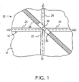
- the optical switch 10 is formed of layers that are patterned on a substrate.
- the waveguide layers on the substrate include an optional lower cladding layer 14, an optical core 16, and an upper cladding layer, not shown.
- the optical core may be primarily silicon dioxide, with doping materials that achieve a desired index of refraction.
- the cladding layers are formed of a material having a refractive index that is significantly different than that of the core material, so that the optical signals are guided along the core.
- the effective phase index of the waveguide is determined by the refractive indices of the core material and the material of the cladding layers.
- the layer of core material is patterned into waveguide segments that define a pair of input waveguides 20 and 24 and a pair of output waveguides 22 and 26.
- the upper cladding layer is blanket deposited.
- a trench 28 is etched into the cladding layers and the core material.
- a liquid having a refractive index that substantially matches the effective phase index of the waveguides is supplied to the trench. When the liquid is aligned with the waveguides, signals will propagate efficiently through the trench. Thus, signals from the input waveguide 20 will exit from the aligned output waveguide 26, while signals from the input waveguide 24 will exit via the aligned output waveguide 22.
- the first input waveguide 20 and the second output waveguide 22 have axes that intersect at or near (preferably near) a sidewall of the trench 28 at an angle of incidence that results in total internal reflection (TIR).
- TIR total internal reflection
- the refractive index mismatch creates the TIR condition in which an input signal along the input waveguide 20 is reflected into the second output waveguide 22.
- the second input waveguide 24 is not optically coupled to either of the output waveguides 22 and 26, since the misalignment of the optical axes of the waveguides inhibits optical coupling.
- the patent to Fouquet et al. describes a number of alternative embodiments for switching the optical switch 10 between a transmissive state and a reflective state.
- the liquid within the trench fills the entire area aligned with the waveguides 20, 22, 24 and 26.
- One approach to switching between the two states is to include a microheater 38 that controls the formation of a bubble 30 within the liquid-containing trench 28.
- the microheater When the microheater is brought to a temperature that is sufficiently high to form the bubble in the index-matching liquid, the bubble is ideally positioned across the entirety of the interface between each waveguide and the sidewall of the trench. In this ideal situation, only a small quantity of the light leaks into the trench.
- the electrical power to the microheaters of optical switches may be increased to deliver ample thermal power to create and maintain the bubbles across the entirety of the interface.
- this solution has limited appeal, since the power handling constraints of a large array of optical switches and because of the desirability of operating such an array at the lowest possible power consumption level.
- Another approach is to appropriately design the shape and size of the trenches holding the bubbles relative to the shapes and sizes of the microheaters which create the bubbles.
- a trench is extended downwardly at opposite sides of the microheater.
- V-shaped cuts are etched into a microheater substrate in alignment with the trench.
- the downward extension of the trench is intended to increase bubble stability by promoting dynamic equilibrium, with fluid boiling at the heaters and condensing at the top of the bubbles. This approach improves stability, but alternative or additional techniques are desired.
- the raised barriers partially obstruct the movement or expansion of the bubble into the adjacent spacing.
- the raised barriers may be partial barriers that are provided by depositing or growing a material, typically a dielectric material, on the heater substrate.
- the barriers are positioned within the adjacent spacing on two opposed sides of the microheater, but may include portions which reside within the trench at the other two sides of the microheater.
- the barrier material may provide longitudinal control along the length of the trench.
- incorporating steps of providing and patterning the barrier material is a relatively small price to pay for the long term reduction (via surface energy variations) or even complete prevention (by physically blocking) of the lateral expansion of a bubble into the spacing that is adjacent to a trench.
- One advantage of the invention is that bubble stability is improved. As a result, the optical performance of the optical switch will be improved. Another advantage is that enhanced stability is achieved without increasing the operating power requirements of the optical switch or the switching array in which the optical switch is a member. While additional processing steps are required, the additional steps are neither complex nor costly.
- Fig. 1 is a top view of an optical switch that utilizes total internal reflectance in accordance with the prior art.
- Fig. 2 is a top view of an optical switch having bubble-positioning surface features in accordance with the invention.
- Fig. 3 is a side sectional view of the optical switch of Fig. 2 taken along lines 3-3.
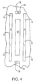
- Fig. 4 is a top view of an alternative application of the bubble-positioning surface features of Figs. 2 and 3.
- Fig. 5 is a side sectional view of the trench region of the optical switch in accordance with one application of an example.
- Fig. 6 is a side sectional view of the trench region of the optical switch in accordance with another embodiment.
- Fig. 7 is a top view of the trench region of the optical switch in accordance with another example.
- Fig. 8 is a side sectional view of the tench region of the optical switch in accordance with a further example.
- Fig. 9 is a side sectional view of the trench region of the optical switch in accordance with still another example.
- Fig. 10 is a side sectional view of the trench region of the optical switch, with a hydrophobic film on the walls of the trench.
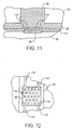
- Fig. 11 is a side sectional view of the trench region of the optical switch in accordance with yet another example.
- Fig. 12 is a top view of the example of Fig. 11.
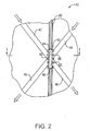
- an optical switch 40 is shown as including many of the features described with reference to Fig. 1.
- the optical switch includes four waveguide segments that will be referred to as first and second input waveguides 42 and 44 and first and second output waveguides 46 and 48. While not evident from the simplified drawings, the waveguides are formed in the conventional manner of encasing core material within upper and lower cladding layers, so that light is guided along the core material.
- Each of the waveguides 42, 44, 46 and 48 has an end that intersects a liquid-containing trench 50.
- the optical switch 40 is shown in a reflective state, since a bubble 52 resides at the region of the trench that is abutted by the waveguides.
- the optical coupling among the waveguides is dependent upon the localized optical characteristics at this crosspoint. With the bubble 52 positioned as shown in Fig. 2, an input signal along waveguide 42 will encounter a mismatch in the refractive index at the sidewall of the trench. As a result, the optical signal will be reflected into the second output waveguide 48.
- the angle of incidence of the waveguides 42, 44, 46 and 48 on the sidewalls of the trench 50 should be greater than the critical angle required for total internal reflection (TIR).
- TIR total internal reflection
- the liquid within the trench 50 has a refractive index that is sufficiently close to the refractive index of the core material used in forming the waveguides that optical signals will freely propagate between the waveguides and the liquid within the trench.
- the bubble 52 is allowed to condense and the liquid flows within the crosspoint region, the first input waveguide 42 will be coupled to the first output waveguide 46, while the second input waveguide 44 will be coupled to the second output waveguide 48.
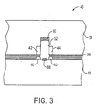
- performance of the optical switch 40 is affected by the position of the bubble 52 relative to the trench-to-waveguide interfaces. If the surface area of the bubble 52 against the trench sidewall fully encompasses the lateral extents of the optical fields of the crossing waveguides, the reflection is at a stable maximum. However, any reduction below this full lateral extension of the optical fields will cause some optical loss. Moreover, if the bubble is unstable in its position, reflective characteristics of the switch will also be unstable. In Figs. 2 and 3, surface features have been incorporated into the switch in order to stabilize the bubble and the switch performance. Other types of surface features will be described with reference to subsequent figures.
- the optical switch 40 is formed of a waveguide substrate 54 and a heater substrate 56.
- the two substrates are bonded together, but are spaced apart along the region adjacent to the trench 50.
- a spacing 58 is formed between the two substrates 54 and 56.
- An advantage of this spacing is that it accommodates any volumetric expansion caused by bubble formation and bubble collapse. However, while it is desirable to accommodate changes in volume, the accommodation should not adversely affect the bubble stability.
- raised barriers 60, 62, 64 and 66 are formed at the different sides of a microheater 68 for forming the bubble 52.
- the lateral barriers 60 and 62 are positioned within the spacing 58 adjacent to the trench 50.
- the longer two barriers control lateral expansion of the bubble 52 into the adjacent spacing 58.
- "Longitudinal control" of the bubble is provided by the end barriers 64 and 66. While these barriers are shown as being contained within the trench 50, if the trench is formed so that it is only slightly greater than that length of the bubble, the end barriers 64 and 66 may also be within the adjacent spacing.
- the barriers 60, 62, 64 and 66 may be formed by depositing or growing a dielectric layer on the heater substrate 56. Photolithographic techniques may be employed, but other conventional approaches may be used. Since the dimensions of the barriers are not critical, relaxed fabrication tolerances are acceptable. A possible material for forming the barriers is silicon dioxide, but other materials may be substituted.
- the barriers may be formed on the waveguide substrate 54.
- the thickness of the barriers may be increased to contact both of the substrates 54 and 56, so that the barriers prevent (by physical blocking) the lateral expansion of the bubble 52, rather than merely reducing (by surface energy variations) the lateral expansion of the bubble into the adjacent spacing 58.
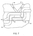
- the barriers may be segmented. This is shown in Fig. 4, which provides three segments 70, 72 and 74 at each of the opposite long sides of the microheater to control lateral expansion of the bubble and provides two segments 76 and 78 at the shorter sides of heater to control longitudinal bubble expansion.
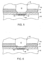
- Fig. 5 illustrates another example to providing bubble stability, performance, and thermal stability within an optical switch.
- the intentional alterations to surface topography are implemented as surface variations along a target boundary line of contact between the bubble 52 and the structure of the optical switch. It is considered beneficial to form the surface variations at the edges of the microheater 68, or at least close to the microheater edges.
- the surface variations may be along the target boundary line of bubble contact with the walls which include the ends of the waveguides or along the target boundary line of bubble contact with the top wall of the waveguide substrate.
- the change in the surface topography "pins" the bubble along the target contact line.
- the surface features are shown as being local depressions 80 and 82 within a dielectric layer 84.
- the dielectric layer may be one that is often used to protect the metallic microheater from chemicals of the index-matching fluid.
- the localized depressions may be isotropic or anisotropic pits formed using conventional photolithographic techniques, since the geometry of the depressions is not a major issue.
- the depressions are replaced with raised regions 86 and 88.
- the raised regions function in the same manner as the localized depressions 80 and 82 of Fig. 5.
- the material used to form the raised regions should have a low thermal conductivity. Photolithographic patterning of a dielectric material adds very little to the cost and complexity of the process for forming an optical switch.
- the depressions 80 and 82 or raised regions 86 and 88 may extend around the entire microheater 68, thereby providing longitudinal stability, as well as the lateral stability.
- the intentionally altered surface features are dielectric-filled cavities 90 and 92 within the surface of the heater substrate.
- the dielectric-filled cavities provide additional thermal insulation, reducing the loss of heat into the heater substrate. As a result, the delivery of heat to the bubble is significantly improved.
- An abrupt transition in heat-conduction conditions provides desired results, so forming substantially vertical cavity walls is beneficial.
- One available approach to forming cavities having substantially vertical walls is referred to as the Bosch process, which uses vacuum and plasma etching (dry etching) techniques. With the abrupt transitions in thermal dynamics that are provided by the vertical walls of the cavities, the addition of the dielectric filler material becomes less important. Consequently, the regions 90 and 92 may be empty cavities in some embodiments.
- the dielectric-filled cavities are shown as two dielectric regions 90 and 92 that follow the curvature of a conductive path 94 along the heater substrate.
- the conductive path 94 is a trace that provides actuator current to the microheater 68.
- the conductive path is a conventional component of a heater substrate of an optical switch.
- the microheater 68 is connected to the underlying conductive path 94, so that the heater can be activated and deactivated based upon supplying current through the conductive path.
- the heater substrate may be formed of silicon, which is etched in a pattern to accommodate the dielectric (or sometimes void) regions 90 and 92.
- the dielectric material has a low thermal conductivity relative to the substrate material. Consequently, the heat from the microheater is less likely to radiate in a pattern that causes the bubble to expand laterally into the substrate-to-substrate spacing.
- the dielectric material may be silicon dioxide or any other material that is nonconductive and that has a significantly lower thermal conductivity than the substrate material.
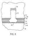
- auxiliary trenches 96 and 98 are formed adjacent to the main trench 50.
- the edges of the auxiliary trenches alter the surface energy balance, so as to inhibit the lateral expansion of the bubble 52.
- the auxiliary trenches 96 and 98 are filled with the index-matching liquid when the switch is in its transmitting state, and since the index-matching liquid has a lower thermal conductivity than the substrate material (e.g., silica or silicon), the auxiliary trenches present a barrier to thermal loss from the heated waveguide crosspoint of the optical switch. Therefore, the auxiliary trenches may help in maintaining the size and position of the thermally created and maintained bubble 52.
- auxiliary trenches 96 and 98 are shown as being formed within a dielectric layer 100 on the surface of the waveguide substrate 54. However, the auxiliary trenches may be formed in the substrate material itself. As a substitute or as an addition to the auxiliary trenches 96 and 98 in the waveguide substrate 54, auxiliary trenches may be formed in the heater substrate 56. An advantage of forming the auxiliary trenches within the heater substrate is that the trenches may be formed in closer alignment with the lateral edges of the main trench 50.
- added layers 102 and 104 on the surfaces of the waveguide substrate 54 and the heater substrate 56 provide the desired surface features within the substrate-to-substrate spacing 58.
- the layers 102 and 104 are designed to provide a target surface wettability within the spacing. The wettability affects the capillary forces at the bubble interface with the liquid within the spacing. Thus, the angle of incidence between the bubble and each layer is more predictable and stable.
- the bulges into the spacing 58 have an angle of incidence that is significantly different than the bulge of the residue index-matching liquid within the top of the trench 50. Capillary action induces forces on the liquid within the spacing 58 to "creep" along the surfaces of the added layers 102 and 104 to the ends of the layers.
- the added layers 102 and 104 are patterned on the two substrates 54 and 56 to only be in the area close to the trench 50.
- the selection of the layer should be such that it provides an intrinsically different wettability to the fluid, relative to the underlying layer.
- the underlying layers may be silicon dioxide layers 106 and 108 and the added layer may be gold.
- the "added" layers may be treatments of the silicon dioxide material.
- the substrates 54 and 56 are silica substrates having silicon oxide films, differences in wettability can be induced by the selective self assembly of organic functionalized orthosilicates or chlorosilanes onto the silicon oxide surface.
- a specific subgroup that achieves target wettability characteristics is fluorinated long chain hydrocarbon chlorosilane.
- the added layer is gold
- selective self assembly of alkane thiols onto the gold surface may provide the target wettability characteristics.
- a specific acceptable subgroup is fluorinated long chain alkane thiol.
- the index-matching fluid includes an additive that does not significantly affect the refractive index of the fluid, but reduces the likelihood that the fluid will attack the layers.
- the added layer may be a polymer, such as a fluorinated polymer.
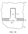
- the trench 50 may be coated with a hydrophobic film 110 to reduce the likelihood that residue liquid will remain along the optical window formed by the interface of the trench 50 and one of the waveguides.
- the residue liquid could adversely affect the performance of the optical switch, since its index-matching properties will allow an input signal to enter for a short distance into the bubble-containing trench that is intended to provide total internal reflection.
- the shape of the residue will affect the induced reflection at the interface of the residue and the bubble.
- the hydrophobic film 110 reduces the likelihood of residue along the optical window.
- the film may be formed of a polymer, such as a fluorinated polymer (e.g., PTFE).
- An additive may be introduced into the index-matching liquid to further promote dewetting.
- the hydrophobic film 110 of Fig. 10 is shown as being used without any of the previously described techniques for controlling bubble expansion within the substrate-to-substrate spacing 58, the film is preferably used with at least one of the other approaches.
- the added layers 102 and 104 may be formed of the same material as the hydrophobic film 110.
- the layers 102 and 104 are preferably formed separately, so that the layers and the film may be individually tailored to achieve their separate goals.
- the different approaches to pinning the bubble may be combined.
- the use of the layers 102 and 104 to enhance capillary forces may be combined with the approach of Fig. 5, where local depressions 80 and 82 are formed at or near the edges of the microheater 68 in order to provide bubble control.
- a thin layer 114 is formed to include capillary holes 118 and cooling fins 116. This layer is shown as being spaced apart from the microheater 68 by a dielectric layer 112, but other arrangements are possible.
- the thin layer may be a metal mesh, sintered metal, or other porous thin layer that is configured to draw fluid toward the microheater by capillary forces. The intent is to increase the portion of the heater region that is wet, thereby increasing the ability of the microheater to provide vaporization as needed. Within the conventional structure, vaporization is confined to the edges of the heater region after the bubble begins to be formed. Bubble stability is enhanced by drawing the liquid toward the heater region for wider area vaporization.
- the cooling fins 116 promote heat dissipation when the microheater is deactivated.
- the thin layer 114 that is configured to induce capillary forces may be formed of gold.
- the gold layer may be electroplated onto the dielectric layer 112 and then etched using conventional photolithographic techniques. However, other materials and other deposition and patterning approaches may be used.
Landscapes
- Physics & Mathematics (AREA)
- General Physics & Mathematics (AREA)
- Optics & Photonics (AREA)
- Mechanical Light Control Or Optical Switches (AREA)
- Micromachines (AREA)
Applications Claiming Priority (2)
| Application Number | Priority Date | Filing Date | Title |
|---|---|---|---|
| US10/099,116 US6798939B2 (en) | 2002-03-14 | 2002-03-14 | Bubble stability in an optical switch |
| US99116 | 2002-03-14 |
Publications (3)
| Publication Number | Publication Date |
|---|---|
| EP1345055A2 EP1345055A2 (en) | 2003-09-17 |
| EP1345055A3 EP1345055A3 (en) | 2004-01-14 |
| EP1345055B1 true EP1345055B1 (en) | 2006-06-21 |
Family
ID=27765441
Family Applications (1)
| Application Number | Title | Priority Date | Filing Date |
|---|---|---|---|
| EP02023226A Expired - Lifetime EP1345055B1 (en) | 2002-03-14 | 2002-10-16 | Bubble stability in an optical switch |
Country Status (4)
| Country | Link |
|---|---|
| US (1) | US6798939B2 (enExample) |
| EP (1) | EP1345055B1 (enExample) |
| JP (1) | JP4248275B2 (enExample) |
| DE (1) | DE60212564T2 (enExample) |
Families Citing this family (7)
| Publication number | Priority date | Publication date | Assignee | Title |
|---|---|---|---|---|
| US7274840B2 (en) * | 2003-07-23 | 2007-09-25 | Avago Technologies Fiber Ip (Singapore) Pte. Ltd. | Clean and test for fluid within a reflection optical switch system |
| US7024062B2 (en) * | 2004-02-25 | 2006-04-04 | John Julian Uebbing | Optical switch with low pressure bubble |
| KR100674866B1 (ko) * | 2005-05-16 | 2007-01-30 | 삼성전기주식회사 | 가변 초점 렌즈 및 그 제조 방법 |
| US20060263613A1 (en) * | 2005-05-20 | 2006-11-23 | General Electric Company | Temperature dependent transparent optical coatings for high temperature absorption |
| US8121487B2 (en) * | 2008-02-05 | 2012-02-21 | Honeywell International Inc. | System and method for free space micro machined optical bench |
| DE102017123522A1 (de) * | 2017-10-10 | 2019-04-11 | Carl Zeiss Meditec Ag | Schaltbare Strahlteilervorrichtung |
| US11733468B2 (en) * | 2021-12-08 | 2023-08-22 | Viavi Solutions Inc. | Photonic structure using optical heater |
Family Cites Families (19)
| Publication number | Priority date | Publication date | Assignee | Title |
|---|---|---|---|---|
| FR2660440B1 (fr) * | 1990-04-03 | 1992-10-16 | Commissariat Energie Atomique | Composant optique integre protege contre l'environnement et son procede de fabrication. |
| JP2828216B2 (ja) | 1990-10-09 | 1998-11-25 | 日立電線株式会社 | 光スイッチ及びその製造方法 |
| JP2871879B2 (ja) | 1991-03-28 | 1999-03-17 | 日立電線株式会社 | 導波路型光スイッチ |
| JP2994807B2 (ja) | 1991-08-29 | 1999-12-27 | 日立電線株式会社 | 導波路型光スイッチ |
| JP2871911B2 (ja) | 1991-09-30 | 1999-03-17 | 日立電線株式会社 | 導波路型光スイッチ |
| US5699462A (en) * | 1996-06-14 | 1997-12-16 | Hewlett-Packard Company | Total internal reflection optical switches employing thermal activation |
| US5852689A (en) * | 1997-04-09 | 1998-12-22 | Hewlett-Packard Company | Method for making fluid optical switches |
| US5960131A (en) * | 1998-02-04 | 1999-09-28 | Hewlett-Packard Company | Switching element having an expanding waveguide core |
| US6195478B1 (en) | 1998-02-04 | 2001-02-27 | Agilent Technologies, Inc. | Planar lightwave circuit-based optical switches using micromirrors in trenches |
| US6171652B1 (en) | 1998-05-26 | 2001-01-09 | Brij P. Singh | Method for modifying surfaces with ultra thin films |
| US6062681A (en) * | 1998-07-14 | 2000-05-16 | Hewlett-Packard Company | Bubble valve and bubble valve-based pressure regulator |
| US6389189B1 (en) * | 1998-10-23 | 2002-05-14 | Corning Incorporated | Fluid-encapsulated MEMS optical switch |
| US6360775B1 (en) * | 1998-12-23 | 2002-03-26 | Agilent Technologies, Inc. | Capillary fluid switch with asymmetric bubble chamber |
| US6487333B2 (en) * | 1999-12-22 | 2002-11-26 | Agilent Technologies, Inc. | Total internal reflection optical switch |
| US6327397B1 (en) * | 2000-02-22 | 2001-12-04 | Agilent Technologies, Inc. | System and method for providing temperature control for a thermally activated optical switch using constant total power |
| US6563973B1 (en) * | 2000-06-27 | 2003-05-13 | Corning Incorporated | Low-index waveguide liquid crystal cross-connect |
| EP1267194A1 (en) | 2001-06-14 | 2002-12-18 | STMicroelectronics S.r.l. | Optical switch |
| US6674933B2 (en) * | 2001-09-27 | 2004-01-06 | Agilent Technologies, Inc. | Optical switch controlled by selective activation and deactivation of an optical source |
| US6718085B1 (en) * | 2002-10-07 | 2004-04-06 | Agilent Technologies, Inc. | Stable optical switch with reduced power consumption |
-
2002
- 2002-03-14 US US10/099,116 patent/US6798939B2/en not_active Expired - Fee Related
- 2002-10-16 DE DE60212564T patent/DE60212564T2/de not_active Expired - Lifetime
- 2002-10-16 EP EP02023226A patent/EP1345055B1/en not_active Expired - Lifetime
-
2003
- 2003-03-14 JP JP2003069541A patent/JP4248275B2/ja not_active Expired - Fee Related
Also Published As
| Publication number | Publication date |
|---|---|
| EP1345055A2 (en) | 2003-09-17 |
| DE60212564T2 (de) | 2007-05-03 |
| US20030174930A1 (en) | 2003-09-18 |
| JP4248275B2 (ja) | 2009-04-02 |
| JP2003315706A (ja) | 2003-11-06 |
| DE60212564D1 (de) | 2006-08-03 |
| US6798939B2 (en) | 2004-09-28 |
| EP1345055A3 (en) | 2004-01-14 |
Similar Documents
| Publication | Publication Date | Title |
|---|---|---|
| KR102427251B1 (ko) | 집적 광학 기반의 광 응력 위상 변조기 | |
| KR101063957B1 (ko) | 폴리머 삽입형 실리카 광도파로를 이용하는 전반사형 광 스위치 및 그의 제조 방법 | |
| EP0935149B1 (en) | Switching element having an expanding waveguide core | |
| US6493482B1 (en) | Optical switch having a planar waveguide and a shutter actuator | |
| WO2001038910A1 (en) | Optical waveguide having a weakly-confining waveguide section and a strongly-confining waveguide section optically coupled by a tapered neck | |
| JP2003131055A (ja) | 光導波路及びその製造方法 | |
| EP1345055B1 (en) | Bubble stability in an optical switch | |
| JP2001021930A (ja) | 熱光学スイッチ、その製作方法及びそれを用いた光線路変更方法 | |
| JP2002006244A (ja) | 効率的な反射結合を行なうための導波路の配置と角度の決定 | |
| JP2003149564A (ja) | 圧力動作する双安定光スイッチング | |
| JP2000206476A (ja) | 温度制御型光導波路 | |
| JP2000187192A (ja) | 温度制御型光導波路 | |
| WO2001059492A2 (en) | Optical waveguide and shutter | |
| JP2004133451A (ja) | 光スイッチ | |
| US6671439B2 (en) | Integrated waveguide arrangement, process for producing an integrated waveguide arrangement, and waveguide components | |
| WO2001048532A9 (en) | Integrated planar optical waveguide and shutter | |
| US6532319B2 (en) | Ceramic substrate for photonic switching system | |
| US6876788B2 (en) | Preventing hydrodynamic crosstalk in an optical switch | |
| US20020176652A1 (en) | Optical device | |
| JP2000221459A (ja) | 温度制御型光導波路 | |
| JP2000121969A (ja) | 光スイッチ | |
| US20050092233A1 (en) | Single and multi-layer crystalline structures | |
| JP2004139080A (ja) | 光経路変更のための光スイッチ及びその動作方法 | |
| Yu et al. | Jingwei Liu | |
| JPH05241034A (ja) | 基板型光結合器 |
Legal Events
| Date | Code | Title | Description |
|---|---|---|---|
| PUAI | Public reference made under article 153(3) epc to a published international application that has entered the european phase |
Free format text: ORIGINAL CODE: 0009012 |
|
| AK | Designated contracting states |
Kind code of ref document: A2 Designated state(s): AT BE BG CH CY CZ DE DK EE ES FI FR GB GR IE IT LI LU MC NL PT SE SK TR |
|
| AX | Request for extension of the european patent |
Extension state: AL LT LV MK RO SI |
|
| PUAL | Search report despatched |
Free format text: ORIGINAL CODE: 0009013 |
|
| AK | Designated contracting states |
Kind code of ref document: A3 Designated state(s): AT BE BG CH CY CZ DE DK EE ES FI FR GB GR IE IT LI LU MC NL PT SE SK TR |
|
| AX | Request for extension of the european patent |
Extension state: AL LT LV MK RO SI |
|
| 17P | Request for examination filed |
Effective date: 20040616 |
|
| AKX | Designation fees paid |
Designated state(s): DE FR GB |
|
| 17Q | First examination report despatched |
Effective date: 20040928 |
|
| GRAP | Despatch of communication of intention to grant a patent |
Free format text: ORIGINAL CODE: EPIDOSNIGR1 |
|
| GRAS | Grant fee paid |
Free format text: ORIGINAL CODE: EPIDOSNIGR3 |
|
| GRAA | (expected) grant |
Free format text: ORIGINAL CODE: 0009210 |
|
| RAP1 | Party data changed (applicant data changed or rights of an application transferred) |
Owner name: AVAGO TECHNOLOGIES GENERAL IP (SINGAPORE) PTE. LTD |
|
| AK | Designated contracting states |
Kind code of ref document: B1 Designated state(s): DE FR GB |
|
| REG | Reference to a national code |
Ref country code: GB Ref legal event code: FG4D |
|
| REG | Reference to a national code |
Ref country code: GB Ref legal event code: 732E |
|
| REF | Corresponds to: |
Ref document number: 60212564 Country of ref document: DE Date of ref document: 20060803 Kind code of ref document: P |
|
| RAP2 | Party data changed (patent owner data changed or rights of a patent transferred) |
Owner name: AVAGO TECHNOLOGIES FIBER IP (SINGAPORE) PTE. LTD. |
|
| ET | Fr: translation filed | ||
| PLBE | No opposition filed within time limit |
Free format text: ORIGINAL CODE: 0009261 |
|
| STAA | Information on the status of an ep patent application or granted ep patent |
Free format text: STATUS: NO OPPOSITION FILED WITHIN TIME LIMIT |
|
| 26N | No opposition filed |
Effective date: 20070322 |
|
| REG | Reference to a national code |
Ref country code: FR Ref legal event code: ST Effective date: 20080630 |
|
| PGFP | Annual fee paid to national office [announced via postgrant information from national office to epo] |
Ref country code: FR Payment date: 20061017 Year of fee payment: 5 |
|
| PG25 | Lapsed in a contracting state [announced via postgrant information from national office to epo] |
Ref country code: FR Free format text: LAPSE BECAUSE OF NON-PAYMENT OF DUE FEES Effective date: 20071031 |
|
| PGFP | Annual fee paid to national office [announced via postgrant information from national office to epo] |
Ref country code: DE Payment date: 20101013 Year of fee payment: 9 |
|
| PG25 | Lapsed in a contracting state [announced via postgrant information from national office to epo] |
Ref country code: DE Free format text: LAPSE BECAUSE OF NON-PAYMENT OF DUE FEES Effective date: 20120501 |
|
| REG | Reference to a national code |
Ref country code: DE Ref legal event code: R119 Ref document number: 60212564 Country of ref document: DE Effective date: 20120501 |
|
| PGFP | Annual fee paid to national office [announced via postgrant information from national office to epo] |
Ref country code: GB Payment date: 20121010 Year of fee payment: 11 |
|
| GBPC | Gb: european patent ceased through non-payment of renewal fee |
Effective date: 20131016 |
|
| PG25 | Lapsed in a contracting state [announced via postgrant information from national office to epo] |
Ref country code: GB Free format text: LAPSE BECAUSE OF NON-PAYMENT OF DUE FEES Effective date: 20131016 |