EP1341242B1 - Dopant comprenant du bore pour un OLED - Google Patents
Dopant comprenant du bore pour un OLED Download PDFInfo
- Publication number
- EP1341242B1 EP1341242B1 EP03075447A EP03075447A EP1341242B1 EP 1341242 B1 EP1341242 B1 EP 1341242B1 EP 03075447 A EP03075447 A EP 03075447A EP 03075447 A EP03075447 A EP 03075447A EP 1341242 B1 EP1341242 B1 EP 1341242B1
- Authority
- EP
- European Patent Office
- Prior art keywords
- host
- dopant
- bis
- group
- layer
- Prior art date
- Legal status (The legal status is an assumption and is not a legal conclusion. Google has not performed a legal analysis and makes no representation as to the accuracy of the status listed.)
- Expired - Lifetime
Links
- 0 C*(*=C(C=C(C)C=C(c1c(*)cccc1)OC)C(N)=C(C(N)=C(C)N)N)(N)N Chemical compound C*(*=C(C=C(C)C=C(c1c(*)cccc1)OC)C(N)=C(C(N)=C(C)N)N)(N)N 0.000 description 8
Images

Classifications
-
- H—ELECTRICITY
- H05—ELECTRIC TECHNIQUES NOT OTHERWISE PROVIDED FOR
- H05B—ELECTRIC HEATING; ELECTRIC LIGHT SOURCES NOT OTHERWISE PROVIDED FOR; CIRCUIT ARRANGEMENTS FOR ELECTRIC LIGHT SOURCES, IN GENERAL
- H05B33/00—Electroluminescent light sources
- H05B33/12—Light sources with substantially two-dimensional radiating surfaces
- H05B33/18—Light sources with substantially two-dimensional radiating surfaces characterised by the nature or concentration of the activator
-
- H—ELECTRICITY
- H10—SEMICONDUCTOR DEVICES; ELECTRIC SOLID-STATE DEVICES NOT OTHERWISE PROVIDED FOR
- H10K—ORGANIC ELECTRIC SOLID-STATE DEVICES
- H10K50/00—Organic light-emitting devices
- H10K50/10—OLEDs or polymer light-emitting diodes [PLED]
- H10K50/11—OLEDs or polymer light-emitting diodes [PLED] characterised by the electroluminescent [EL] layers
-
- H—ELECTRICITY
- H10—SEMICONDUCTOR DEVICES; ELECTRIC SOLID-STATE DEVICES NOT OTHERWISE PROVIDED FOR
- H10K—ORGANIC ELECTRIC SOLID-STATE DEVICES
- H10K85/00—Organic materials used in the body or electrodes of devices covered by this subclass
- H10K85/30—Coordination compounds
- H10K85/321—Metal complexes comprising a group IIIA element, e.g. Tris (8-hydroxyquinoline) gallium [Gaq3]
-
- H—ELECTRICITY
- H10—SEMICONDUCTOR DEVICES; ELECTRIC SOLID-STATE DEVICES NOT OTHERWISE PROVIDED FOR
- H10K—ORGANIC ELECTRIC SOLID-STATE DEVICES
- H10K85/00—Organic materials used in the body or electrodes of devices covered by this subclass
- H10K85/30—Coordination compounds
- H10K85/341—Transition metal complexes, e.g. Ru(II)polypyridine complexes
- H10K85/342—Transition metal complexes, e.g. Ru(II)polypyridine complexes comprising iridium
-
- H—ELECTRICITY
- H10—SEMICONDUCTOR DEVICES; ELECTRIC SOLID-STATE DEVICES NOT OTHERWISE PROVIDED FOR
- H10K—ORGANIC ELECTRIC SOLID-STATE DEVICES
- H10K85/00—Organic materials used in the body or electrodes of devices covered by this subclass
- H10K85/30—Coordination compounds
- H10K85/351—Metal complexes comprising lanthanides or actinides, e.g. comprising europium
-
- H—ELECTRICITY
- H10—SEMICONDUCTOR DEVICES; ELECTRIC SOLID-STATE DEVICES NOT OTHERWISE PROVIDED FOR
- H10K—ORGANIC ELECTRIC SOLID-STATE DEVICES
- H10K85/00—Organic materials used in the body or electrodes of devices covered by this subclass
- H10K85/60—Organic compounds having low molecular weight
- H10K85/615—Polycyclic condensed aromatic hydrocarbons, e.g. anthracene
-
- H—ELECTRICITY
- H10—SEMICONDUCTOR DEVICES; ELECTRIC SOLID-STATE DEVICES NOT OTHERWISE PROVIDED FOR
- H10K—ORGANIC ELECTRIC SOLID-STATE DEVICES
- H10K85/00—Organic materials used in the body or electrodes of devices covered by this subclass
- H10K85/60—Organic compounds having low molecular weight
- H10K85/631—Amine compounds having at least two aryl rest on at least one amine-nitrogen atom, e.g. triphenylamine
-
- H—ELECTRICITY
- H10—SEMICONDUCTOR DEVICES; ELECTRIC SOLID-STATE DEVICES NOT OTHERWISE PROVIDED FOR
- H10K—ORGANIC ELECTRIC SOLID-STATE DEVICES
- H10K85/00—Organic materials used in the body or electrodes of devices covered by this subclass
- H10K85/60—Organic compounds having low molecular weight
- H10K85/649—Aromatic compounds comprising a hetero atom
-
- Y—GENERAL TAGGING OF NEW TECHNOLOGICAL DEVELOPMENTS; GENERAL TAGGING OF CROSS-SECTIONAL TECHNOLOGIES SPANNING OVER SEVERAL SECTIONS OF THE IPC; TECHNICAL SUBJECTS COVERED BY FORMER USPC CROSS-REFERENCE ART COLLECTIONS [XRACs] AND DIGESTS
- Y10—TECHNICAL SUBJECTS COVERED BY FORMER USPC
- Y10S—TECHNICAL SUBJECTS COVERED BY FORMER USPC CROSS-REFERENCE ART COLLECTIONS [XRACs] AND DIGESTS
- Y10S428/00—Stock material or miscellaneous articles
- Y10S428/917—Electroluminescent
Definitions
- This invention relates to organic light emitting diode (OLED) electroluminescent (EL) device comprising a light-emitting layer containing a boron dopant compound containing a bis(azinyl)methene boron group.
- OLED organic light emitting diode
- EL electroluminescent
- an organic EL device is comprised of an anode for hole injection, a cathode for electron injection, and an organic medium sandwiched between these electrodes to support charge recombination that yields emission of light. These devices are also commonly referred to as organic light-emitting diodes, or OLEDs.
- organic EL devices are Gurnee et al. U.S. Pat. No. 3,172,862, issued Mar. 9, 1965 ; Gurnee U.S. Pat. No. 3,173,050, issued Mar.
- More recent organic EL devices include an organic EL element consisting of extremely thin layers (e.g. ⁇ 1.0 ⁇ m ) between the anode and the cathode.
- the organic EL element encompasses the layers between the anode and cathode electrodes. Reducing the thickness lowered the resistance of the organic layer and has enabled devices that operate at much lower voltage.
- one organic layer of the EL element adjacent to the anode is specifically chosen to transport holes, therefore, it is referred to as the hole-transporting layer, and the other organic layer is specifically chosen to transport electrons, referred to as the electron-transporting layer.
- the interface between the two layers provides an efficient site for the recombination of the injected hole/electron pair and the resultant electroluminescence.
- the light-emitting layer commonly consists of a host material doped with a guest material - dopant, which results in an efficiency improvement and allows color tuning.
- organic EL device components such as dopants
- a useful class of dopants is derived from the 5,6,5-tricyclic pyrromethene-BF2 complexes and disclosed in EP-A-1 000 998 , US 5,683,823 ; JP 09,289,081A ; and JP 11,097,180A . These materials are characterized by typically narrow emission spectra, which may result in attractively high color purity. However, the green-emitting unsubstituted or alkyl substituted pyrromethene-BF2 complexes exhibit relatively low quantum efficiencies of electroluminescence. In order to achieve highly efficient OLEDs, one needs to use phenyl rings as substituents thereby extending the conjugated ⁇ -system.
- the emission wavelength typically becomes red-shifted yielding a reddish amber color, which is the shortest wavelength light that can be emitted by pyrromethene-BF2 complexes with good efficiency.
- luminance efficient green OLEDs do not appear to be conveniently obtained with pyrromethene BF 2 complexes used as dopants.
- the invention provides an OLED device comprising a light-emitting layer containing a host and a dopant where the dopant comprises a boron compound represented by formula (1) below.
- Such a device exhibits improved luminance efficiency.
- FIG. 1 shows a cross-section of a typical OLED device in which this invention may be used.
- the invention is generally as described above.
- An OLED device of the invention is a multilayer electroluminescent device comprising a cathode, an anode, charge-injecting layers (if necessary), charge-transporting layers, and a light-emitting layer (LEL) comprising a host and at least one dopant, a bis(azinyl)methene boron compound of formula (1).
- LEL light-emitting layer
- azine or azinyl refers to a six-membered aromatic ring system containing at least one nitrogen as defined by the Hantzsch-Widman stems [ The Naming and Indexing of Chemical Substances for Chemical Abstracts-A Reprint of Index IV (Chemical Substance Index Names) from the Chemical Abstracts - 1992 Index Guide; American Chemical Society: Columbus, OH, 1992 ; paragraph 146].
- the light-emitting layer of the device comprises a host and dopant where the dopant is present in an amount of up to 10 wt % of the host, more typically from 0.1-5.0 wt % of the host.
- the group is suitably a 6,6,6-tricyclic bis(azinyl)methene boron complex group, and usefully a bis(pyridinyl) methene boron complex group. Good results are obtained when at least one or both of the pyridyl groups are substituted, particularly where at least one or both of the pyridyl groups has substituent groups joined to form a fused ring.
- Desirable hosts include those based on a chelated oxinoid compound or an anthracene compound. Particular examples of hosts are tris(8-quinolinolato) aluminum (III) and 2- tert -butyl-9,10-di-(2-naphthyl)anthracene.
- Embodiments of the dopants useful in the invention provide an emitted light having a green hue. Substituents are selected to provide embodiments that exhibit a reduced loss of initial luminance compared to the device containing no boron compound of claim 1.
- a and A' represent independent azine ring systems corresponding to 6-membered aromatic ring systems containing at least one nitrogen; each X a and X b is an independently selected substituent, two of which may join to form a fused ring to A or A'; m and n are independently 0 to 4 ; Y is H or a substituent selected from alkyl, aryl and heterocyclic groups; Z a and Z b are fluoro; and 1, 2, 3, 4, 1', 2', 3' , and 4' are independently selected as either carbon or nitrogen atoms.
- 1, 2, 3, 4, 1', 2', 3' , and 4' are conveniently all carbon atoms.
- the device may desirably contain at least one or both of ring A or A' that contains substituents joined to form a fused ring.
- the emission wavelength of these compounds may be adjusted to some extent by appropriate substitution around the central bis(azinyl)methene boron group to meet a color aim, namely green.
- the bis(azinyl)methene boron compound is usually doped into a host compound, which represents the light-emitting layer between the hole-transporting and electron-transporting layers.
- the host is chosen such that there is efficient energy transfer from the host to the bis(azinyl)methene boron compound.
- the bis(azinyl)methene boron complex emits from the excited state to afford a bright, highly-efficient, stable EL device.
- the EL device of the invention is useful in any device where light emission is desired such as a lamp or a component in a static or motion imaging device, such as a television, cell phone, DVD player, or computer monitor.
- Embodiments of the invention provide not only improved luminance efficiency but also improved stability under load and a more desirable green hue as evidenced by the location and shape of the absorption curve of the emitted light.
- substituted or “substituent” means any group or atom other than hydrogen (what about deuterium).
- group when the term “group” is used, it means that when a substituent group contains a substitutable hydrogen, it is also intended to encompass not only the substituent's unsubstituted form, but also its form further substituted with any substituent group or groups as herein mentioned, so long as the substituent does not destroy properties necessary for device utility.
- a substituent group may be halogen or may be bonded to the remainder of the molecule by an atom of carbon, silicon, oxygen, nitrogen, phosphorous, sulfur, selenium, or boron.
- the substituent may be, for example, halogen, such as chloro, bromo or fluoro; nitro; hydroxyl; cyano; carboxyl; or groups which may be further substituted, such as alkyl, including straight or branched chain or cyclic alkyl, such as methyl, trifluoromethyl, ethyl, t -butyl, 3-(2,4-di- t -pentylphenoxy) propyl, and tetradecyl; alkenyl, such as ethylene, 2-butene; alkoxy, such as methoxy, ethoxy, propoxy, butoxy, 2-methoxyethoxy, sec -butoxy, hexyloxy, 2-ethylhexyloxy, tetradecyloxy, 2-(2,4-di- t -pentylphenoxy)ethoxy, and 2-dodecyloxyethoxy; aryl such as phenyl, 4- t
- quaternary ammonium such as triethylammonium
- quaternary phosphonium such as triphenylphosphonium
- silyloxy such as trimethylsilyloxy.
- the substituents may themselves be further substituted one or more times with the described substituent groups.
- the particular substituents used may be selected by those skilled in the art to attain the desired desirable properties for a specific application and can include, for example, electron-withdrawing groups, electron-donating groups, and steric groups.
- the substituents may be joined together to form a ring such as a fused ring unless otherwise provided.
- the above groups and substituents thereof may include those having up to 48 carbon atoms, typically 1 to 36 carbon atoms and usually less than 24 carbon atoms, but greater numbers are possible depending on the particular substituents selected.
- the present invention can be employed in most OLED device configurations. These include very simple structures comprising a single anode and cathode to more complex devices, such as passive matrix displays comprised of orthogonal arrays of anodes and cathodes to form pixels, and active-matrix displays where each pixel is controlled independently, for example, with a thin film transistor (TFT).
- TFT thin film transistor
- FIG. 1 A more typical structure is shown in Figure 1 and contains a substrate 101 , an anode 103 , an optional hole-injecting layer 105 , a hole-transporting layer 107 , a light-emitting layer 109 , an electron-transporting layer 111 , and a cathode 113 . These layers are described in detail below. Note that the substrate may alternatively be located adjacent to the cathode, or the substrate may actually constitute the anode or cathode. Also, the total combined thickness of the organic layers is preferably less than 500 nm.
- the substrate 101 can either be light transmissive or opaque, depending on the intended direction of light emission.
- the light transmissive property is desirable for viewing the EL emission through the substrate.
- Transparent glass or organic material are commonly employed in such cases.
- the transmissive characteristic of the bottom support is immaterial, and therefore can be light transmissive, light absorbing or light reflective.
- Substrates for use in this case include, but are not limited to, glass, plastic, semiconductor materials, ceramics, and circuit board materials. Of course it is necessary to provide in these device configurations a light-transparent top electrode.
- the conductive anode layer 103 is commonly formed over the substrate and, when EL emission is viewed through the anode, should be transparent or substantially transparent to the emission of interest.
- Common transparent anode materials used in this invention are indium-tin oxide (ITO) and tin oxide, but other metal oxides can work including, but not limited to, aluminum- or indium-doped zinc oxide (IZO), magnesium-indium oxide, and nickel-tungsten oxide.
- ITO indium-tin oxide
- IZO aluminum- or indium-doped zinc oxide
- IZO aluminum- or indium-doped zinc oxide
- nickel-tungsten oxide nickel-tungsten oxide.
- metal nitrides such as gallium nitride
- metal selenides such as zinc selenide
- metal sulfides such as zinc sulfide
- the transmissive characteristics of layer 103 are immaterial and any conductive material can be used, transparent, opaque or reflective.
- Example conductors for this application include, but are not limited to, gold, iridium, molybdenum, palladium, and platinum.
- Typical anode materials, transmissive or otherwise, have a work function of 4.1 eV or greater. Desired anode materials are commonly deposited by any suitable means such as evaporation, sputtering, chemical vapor deposition, or electrochemical means. Anodes can be patterned using well-known photolithographic processes.
- HIL Hole-Injecting Layer
- a hole-injecting layer 105 be provided between anode 103 and hole-transporting layer 107 .
- the hole-injecting material can serve to improve the film formation property of subsequent organic layers and to facilitate injection of holes into the hole-transporting layer.
- Suitable materials for use in the hole-injecting layer include, but are not limited to, porphyrinic compounds such as those described in US 4,720,432 , and plasma-deposited fluorocarbon polymers such as those described in US 6,208,075 .
- Alternative hole-injecting materials reportedly useful in organic EL devices are described in EP 0 891 121 A1 and EP 1 029 909 A1 .
- HTL Hole-Transporting Layer
- the hole-transporting layer 107 of the organic EL device contains at least one hole-transporting compound such as an aromatic tertiary amine, where the latter is understood to be a compound containing at least one trivalent nitrogen atom that is bonded only to carbon atoms, at least one of which is a member of an aromatic ring.
- the aromatic tertiary amine can be an arylamine, such as a monoarylamine, diarylamine, triarylamine, or a polymeric arylamine group. Exemplary monomeric triarylamines are illustrated by Klupfel et al. US 3,180,730 .
- Other suitable triarylamines substituted with one or more vinyl radicals and/or comprising at least one active hydrogen containing group are disclosed by Brantley et al US 3,567,450 and US 3,658,520 .
- a more preferred class of aromatic tertiary amines are those which include at least two aromatic tertiary amine moieties as described in US 4,720,432 and US 5,061,569 .
- Such compounds include those represented by structural formula (A). wherein Q 1 and Q 2 are independently selected aromatic tertiary amine moieties and G is a linking group such as an arylene, cycloalkylene, or alkylene group of a carbon to carbon bond.
- at least one of Q 1 or Q 2 contains a polycyclic fused ring group, e.g., a naphthalene.
- G is an aryl group, it is conveniently a phenylene, biphenylene, or naphthalene group.
- a useful class of triarylamine groups satisfying structural formula (A) and containing two triarylamine groups is represented by structural formula (B): where R 1 and R 2 each independently represents a hydrogen atom, an aryl group, or an alkyl group or R 1 and R 2 together represent the atoms completing a cycloalkyl group; and R 3 and R 4 each independently represents an aryl group, which is in turn substituted with a diaryl substituted amino group, as indicated by structural formula (C): wherein R 5 and R 6 are independently selected aryl groups.
- at least one of R 5 or R 6 contains a polycyclic fused ring group, e.g., a naphthalene.
- tetraaryldiamines Another class of aromatic tertiary amine groups are the tetraaryldiamines. Desirable tetraaryldiamines groups include two diarylamino groups, such as indicated by formula (C), linked through an arylene group. Useful tetraaryldiamines include those represented by formula (D). wherein each Are is an independently selected arylene group, such as a phenylene or anthracene group, n is an integer of from 1 to 4, and Ar, R 7 , R 8 , and R 9 are independently selected aryl groups. In a typical embodiment, at least one of Ar, R 7 , R 8 , and R 9 is a polycyclic fused ring group, e.g., a naphthalene
- the various alkyl, alkylene, aryl, and arylene groups of the foregoing structural formulae (A), (B), (C), (D), can each in turn be substituted.
- Typical substituents include alkyl groups, alkoxy groups, aryl groups, aryloxy groups, and halogen such as fluoride, chloride, and bromide.
- the various alkyl and alkylene groups typically contain from 1 to 6 carbon atoms.
- the cycloalkyl moieties can contain from 3 to 10 carbon atoms, but typically contain five, six, or seven ring carbon atoms--e.g., cyclopentyl, cyclohexyl, and cycloheptyl ring structures.
- the aryl and arylene groups are usually phenyl and phenylene moieties.
- the hole-transporting layer can be formed of a single or a mixture of aromatic tertiary amine compounds.
- a triarylamine such as a triarylamine satisfying the formula (B)
- a tetraaryldiamine such as indicated by formula (D).
- a triarylamine is employed in combination with a tetraaryldiamine, the latter is positioned as a layer interposed between the triarylamine and the electron injecting and transporting layer.
- useful aromatic tertiary amines are the following:
- Another class of useful hole-transporting materials includes polycyclic aromatic compounds as described in EP 1 009 041 .
- polymeric hole-transporting materials can be used such as poly( N -vinylcarbazole) (PVK), polythiophenes, polypyrrole, polyaniline, and copolymers such as poly(3,4-ethylenedioxythiophene) / poly(4-styrenesulfonate) also called PEDOT/PSS.
- the light-emitting layer (LEL) 109 of the organic EL element comprises a luminescent or fluorescent material where electroluminescence is produced as a result of electron-hole pair recombination in this region.
- the light-emitting layer can be comprised of a single material, but more commonly consists of a host material doped with a guest compound or compounds where light emission comes primarily from the dopant and can be of any color.
- the host materials in the light-emitting layer can be an electron-transporting material, as defined below, a hole-transporting material, as defined above, or another material or combination of materials that support hole-electron recombination.
- the dopant is usually chosen from highly fluorescent dyes, but phosphorescent compounds, e.g., transition metal complexes as described in WO 98/55561 , WO 00/18851 , WO 00/57676 , and WO 00/70655 are also useful. Dopants are typically coated as 0.01 to 10 % by weight into the host material.
- Host and emitting molecules known to be of use include, but are not limited to, those disclosed in US 4,768,292 , US 5,141,671 , US 5,150,006 , US 5,151,629 , US 5,405,709 , US 5,484,922 , US 5,593,788 , US 5,645,948 , US 5,683,823 , US 5,755,999 , US 5,928,802 , US 5,935,720 , US 5,935,721 , and US 6,020,078 .
- Form E Metal complexes of 8-hydroxyquinoline and similar derivatives constitute one class of useful host compounds capable of supporting electroluminescence, and are particularly suitable for light emission of wavelengths longer than 500 nm, e.g., green, yellow, orange, and red.
- M represents a metal
- n is an integer of from 1 to 4
- Z independently in each occurrence represents the atoms completing a nucleus having at least two fused aromatic rings.
- the metal can be monovalent, divalent, trivalent, or tetravalent metal.
- the metal can, for example, be an alkali metal, such as lithium, sodium, or potassium; an alkaline earth metal, such as magnesium or calcium; an earth metal, such aluminum or gallium, or a transition metal such as zinc or zirconium.
- alkali metal such as lithium, sodium, or potassium
- alkaline earth metal such as magnesium or calcium
- earth metal such aluminum or gallium, or a transition metal such as zinc or zirconium.
- any monovalent, divalent, trivalent, or tetravalent metal known to be a useful chelating metal can be employed.
- Z completes a heterocyclic nucleus containing at least two fused aromatic rings, at least one of which is an azole or azine ring. Additional rings, including both aliphatic and aromatic rings, can be fused with the two required rings, if required. To avoid adding molecular bulk without improving on function the number of ring atoms is usually maintained at 18 or less.
- Illustrative of useful chelated oxinoid compounds are the following:
- Formula F Derivatives of 9,10-di-(2-naphthyl)anthracene (Formula F) constitute one class of useful hosts capable of supporting electroluminescence, and are particularly suitable for light emission of wavelengths longer than 400 nm, e.g., blue, green, yellow, orange or red.
- R 1 , R 2 , R 3 , R 4 , R 5 , and R 6 represent hydrogen or one or more substituents selected from the following groups:
- Illustrative examples include 9,10-di-(2-naphthyl)anthracene and 2- t -butyl-9,10-di-(2-naphthyl)anthracene.
- Other anthracene derivatives can be useful as a host in the LEL, including derivatives of 9,10-bis[4-(2,2-diphenylethenyl)phenyl]anthracene, and phenylanthracene derivatives as described in EP 681,019 .
- Benzazole derivatives constitute another class of useful hosts capable of supporting electroluminescence, and are particularly suitable for light emission of wavelengths longer than 400 nm, e.g., blue, green, yellow, orange or red.
- An example of a useful benzazole is 2, 2', 2"-(1,3,5-phenylene)tris[1-phenyl-1H-benzimidazole].
- Distyrylarylene derivatives as described in US 5,121,029 are also useful host materials in the LEL.
- Desirable fluorescent dopants include groups derived from fused ring, heterocyclic and other compounds such as anthracene, tetracene, xanthene, perylene, rubrene, coumarin, rhodamine, quinacridone, dicyanomethylenepyran, thiopyran , polymethine, pyrilium thiapyrilium, and carbostyryl compounds.
- Illustrative examples of useful dopants include, but are not limited to, the following: X R1 R2 X R1 R2 L9 O H H L23 O H H L10 O H Methyl L24 O H Methyl L11 O Methyl H L25 O Methyl H L12 O Methyl Methyl L26 O Methyl Methyl L13 O H t-butyl L27 O H t-butyl L14 O t-butyl H L28 O t-butyl H L15 O t-butyl t-butyl L29 O t-butyl t-butyl L16 S H H L30 S H H L17 S H Methyl L31 S H Methyl L18 S Methyl H L32 S Methyl H L19 S Methyl Methyl L33 S Methyl Methyl L20 S H t-butyl L34 S H t-butyl L21 S
- ETL Electron-Transporting Layer
- Preferred thin film-forming materials for use in forming the electron-transporting layer 111 of the organic EL devices of this invention are metal chelated oxinoid compounds, including chelates of oxine itself (also commonly referred to as 8-quinolinol or 8-hydroxyquinoline). Such compounds help to inject and transport electrons and exhibit both high levels of performance and are readily fabricated in the form of thin films.
- exemplary of contemplated oxinoid compounds are those satisfying structural formula (E), previously described.
- electron-transporting materials include various butadiene derivatives as disclosed in US 4,356,429 and various heterocyclic optical brighteners as described in US 4,539,507 .
- Benzazoles satisfying structural formula (G) are also useful electron transporting materials.
- layers 109 and 111 can optionally be collapsed into a single layer that serves the function of supporting both light emission and electron transportation.
- the cathode layer 113 used in this invention can be comprised of nearly any conductive material. Desirable materials have good film-forming properties to ensure good contact with the underlying organic layer, promote electron injection at low voltage, and have good stability. Useful cathode materials often contain a low work function metal ( ⁇ 4.0 eV) or metal alloy. One preferred cathode material is comprised of a Mg:Ag alloy wherein the percentage of silver is in the range of 1 to 20 %, as described in US 4,885,221 . Another suitable class of cathode materials includes bilayers comprised of a thin layer of a low work function metal or metal salt capped with a thicker layer of conductive metal.
- cathode is comprised of a thin layer of LiF followed by a thicker layer of A1 as described in US 5,677,572 .
- Other useful cathode materials include, but are not limited to, those disclosed in US 5,059,861 , US 5,059,862 , and US 6,140,763 .
- cathode When light emission is viewed through the cathode, the cathode must be transparent or nearly transparent. For such applications, metals must be thin or one must use transparent conductive oxides, or a combination of these materials.
- Optically transparent cathodes have been described in more detail in US 5,776,623 .
- Cathode materials can be deposited by evaporation, sputtering, or chemical vapor deposition. When needed, patterning can be achieved through many well known methods including, but not limited to, through-mask deposition, integral shadow masking as described in US 5,276,380 and EP 0 732 868 , laser ablation, and selective chemical vapor deposition.
- the organic materials mentioned above are suitably deposited through sublimation, but can be deposited from a solvent with an optional binder to improve film formation. If the material is a polymer, solvent deposition is usually preferred.
- the material to be deposited by sublimation can be vaporized from a sublimator "boat" often comprised of a tantalum material, e.g., as described in US 6,237,529 , or can be first coated onto a donor sheet and then sublimed in closer proximity to the substrate. Layers with a mixture of materials can utilize separate sublimator boats or the materials can be pre-mixed and coated from a single boat or donor sheet.
- Patterned deposition can be achieved using shadow masks, integral shadow masks ( US 5,294,870 ), spatially-defined thermal dye transfer from a donor sheet ( US 5,851,709 and US 6,066,357 ) and inkjet method ( US 6,066,357 ).
- OLED devices are sensitive to moisture and/or oxygen so they are commonly sealed in an inert atmosphere such as nitrogen or argon, along with a desiccant such as alumina, bauxite, calcium sulfate, clays, silica gel, zeolites, alkaline metal oxides, alkaline earth metal oxides, sulfates, or metal halides and perchlorates.
- a desiccant such as alumina, bauxite, calcium sulfate, clays, silica gel, zeolites, alkaline metal oxides, alkaline earth metal oxides, sulfates, or metal halides and perchlorates.
- a glass substrate coated with an 85 nm layer of indium-tin oxide (ITO) as the anode was sequentially ultrasonicated in a commercial detergent, rinsed in deionized water, degreased in toluene vapor and exposed to oxygen plasma for about 1 min.
- ITO indium-tin oxide
- the above sequence completed the deposition of the EL device.
- the device was then hermetically packaged in a dry glove box for protection against ambient environment.
- Samples 2 and 3 were EL devices incorporating Inv-4 or Inv-5 fabricated in an identical manner as the example incorporating Inv-1.
- Sample 4 is a comparative device that was prepared omitting Inv-1 from the LEL and maintaining the same device architecture as in the inventive examples. The cells thus formed were tested for efficiency (in the form of luminance yield), and the results are listed in Table 1. Table 1. Evaluation Results for EL devices.
- EL devices containing bis(azinyl)methene boron complexes In addition to the high luminance yields demonstrated by EL devices containing bis(azinyl)methene boron complexes, the stability of these EL devices also appears to be increased over that of a device without that material.
- a series of EL devices (Samples 5-9) containing Inv-1 and TBADN and a comparative device (Sample 10) without Inv-1 were prepared and subjected to a constant current density of 20 mA/cm 2 at 70 °C. The percent loss of initial luminance was measured after 300 hours, and the results are reported in Table 2. As can be seen from the data, the EL devices containing Inv-1 retain far more of their initial luminance intensity than did the comparative example, with an average improvement of about 35%. Table 2.
- a glass substrate coated with an 85 nm layer of indium-tin oxide (ITO) as the anode was sequentially ultrasonicated in a commercial detergent, rinsed in deionized water, degreased in toluene vapor and exposed to oxygen plasma for about 1 min.
- ITO indium-tin oxide
- the above sequence completed the deposition of the EL device.
- the device was then hermetically packaged in a dry glove box for protection against ambient environment.
- a comparative device was prepared as Sample 12 omitting Inv-1 from the light-emitting layer and maintaining the same device architecture as this example.
- the cells thus formed were tested for efficiency (in the form of luminance yield), and the results are listed in Table 3.
- Sample Host Dopant Efficiency (cd/A) 1 Type 11 AlQ 3 Inv-1 10.39 Invention 12 " None 3.40 Comparison 1 Luminance yields reported at 20 mA/cm 2
- the tested EL device incorporating the INV dopant in an AlQ 3 host demonstrates a superior luminance yield relative to the comparative device.
- the inventive device exhibited green emission ( ⁇ max of 540 nm) with a well-defined vibronic structure and narrow emission peaks as opposed to the very broad AlQ 3 emission at 540 nm.
- Embodiments of the invention include the device wherein the boron complex group is a bis(pyridinyl)methene boron complex group; wherein at least one of the pyridyl groups is substituted; wherein at least one of the pyridyl groups has substituent groups joined to form a fused ring; and where the substituents are selected to provide a reduced loss of initial luminance compared to the device containing no boron compound.
- Embodiments also include the device of formula (1) wherein 1, 2, 3, 4, 1', 2', 3' , and 4' are all carbon atoms; wherein at least one of ring A or A' contains substituents joined to form a fused ring; wherein both ring A and A' contain substituents joined to form a fused ring; wherein there is present at least one X a or X b group selected from the group consisting of halide and alkyl, aryl, alkoxy, and aryloxy groups; and wherein Z a and Z b are F.
- the invention also includes a method of emitting light comprising subjecting the OLED device to an applied voltage.
Claims (7)
- Dispositif OLED comportant une couche émettrice de lumière émettant une lumière verte comprenant un hôte et un dopant, caractérisé en ce que le dopant comprend un composé de bore représenté par la formule (1) :
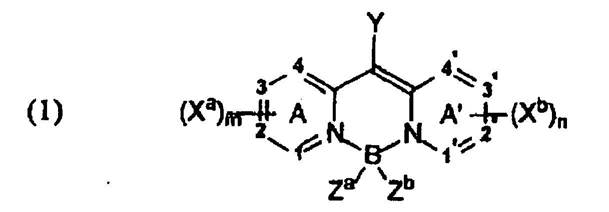
A et A' représentent des systèmes de cycles azine indépendants correspondant à des systèmes de cycles aromatiques à 6 éléments contenant au moins un azote ;
chaque Xa et Xb est un substituant indépendamment choisi, deux desquels peuvent être joints pour former un cycle fusionné à A ou A' ;
m et n sont indépendamment 0 à 4 ;
Y est un H ou un substituant choisi parmi des groupes alkyle, aryle et hétérocycliques ;
Za et Zb sont des fluoro ;
1, 2, 3, 4, 1', 2', 3' et 4' sont indépendamment choisis comme des atomes de carbone ou d'azote. - Dispositif selon la revendication 1, dans lequel la couche comprend un hôte et un dopant, où le dopant est présent dans une quantité de jusqu'à 10 % en poids de l'hôte.
- Dispositif selon la revendication 2, dans lequel le dopant est présent dans une quantité de 0,1 à 5,0 % en poids de l'hôte.
- Dispositif selon la revendication 1, dans lequel l'hôte comprend un composé d'anthracène.
- Dispositif selon la revendication 1, dans lequel l'hôte comprend un composé d'oxynoïde chelaté.
- Dispositif selon la revendication 1, dans lequel l'hôte comprend du tris(8-quinolinolato)aluminium (III) ou du 2-tert-butyl-9,10-di-(2-naphtyl)anthracène.
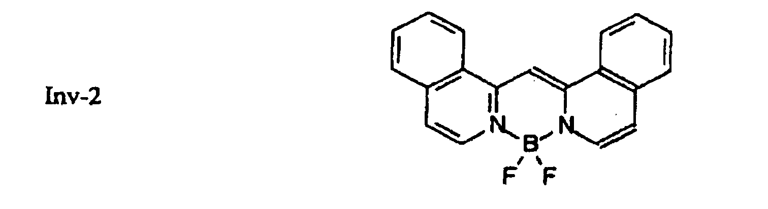
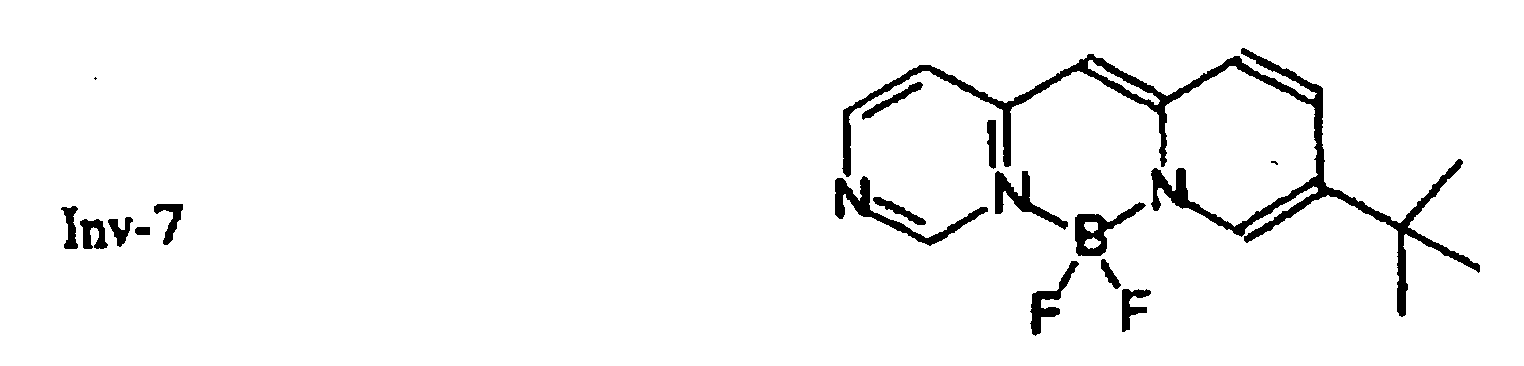
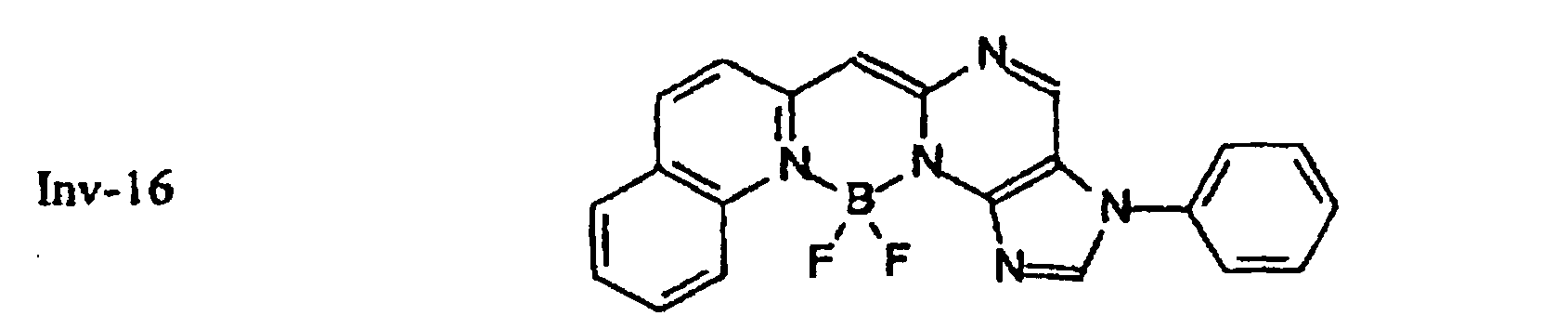
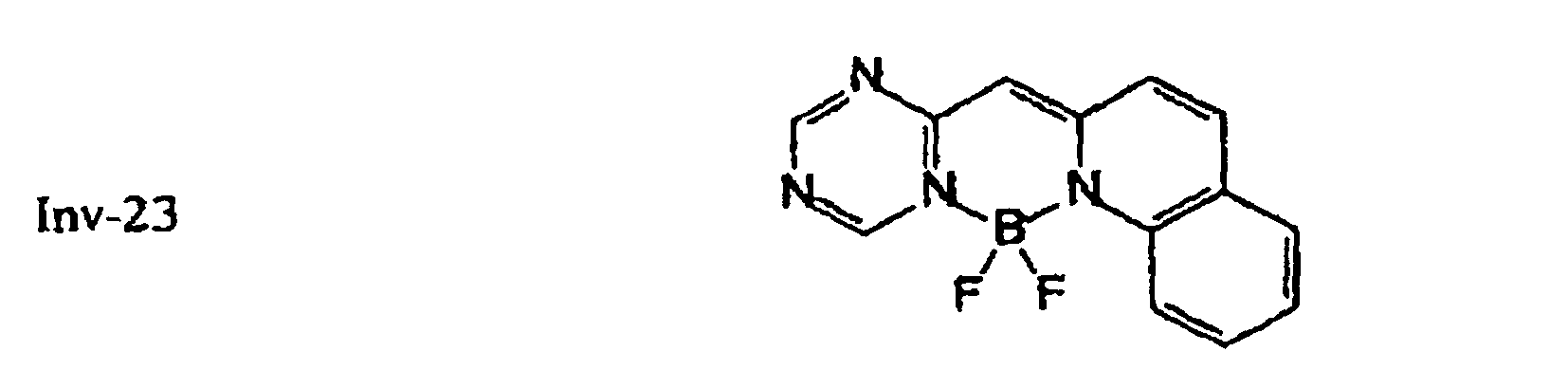
- Dispositif selon la revendication 1, dans lequel le composé de bore est choisi parmi les suivants


Applications Claiming Priority (2)
| Application Number | Priority Date | Filing Date | Title |
|---|---|---|---|
| US86067 | 2002-02-28 | ||
| US10/086,067 US6824893B2 (en) | 2002-02-28 | 2002-02-28 | Organic element for electroluminescent devices |
Publications (3)
| Publication Number | Publication Date |
|---|---|
| EP1341242A2 EP1341242A2 (fr) | 2003-09-03 |
| EP1341242A3 EP1341242A3 (fr) | 2006-06-14 |
| EP1341242B1 true EP1341242B1 (fr) | 2010-06-02 |
Family
ID=27733405
Family Applications (1)
| Application Number | Title | Priority Date | Filing Date |
|---|---|---|---|
| EP03075447A Expired - Lifetime EP1341242B1 (fr) | 2002-02-28 | 2003-02-17 | Dopant comprenant du bore pour un OLED |
Country Status (7)
| Country | Link |
|---|---|
| US (1) | US6824893B2 (fr) |
| EP (1) | EP1341242B1 (fr) |
| JP (1) | JP4050634B2 (fr) |
| KR (1) | KR20030071557A (fr) |
| CN (1) | CN100483775C (fr) |
| DE (1) | DE60332787D1 (fr) |
| TW (1) | TWI268285B (fr) |
Families Citing this family (35)
| Publication number | Priority date | Publication date | Assignee | Title |
|---|---|---|---|---|
| KR100721656B1 (ko) | 2005-11-01 | 2007-05-23 | 주식회사 엘지화학 | 유기 전기 소자 |
| AU2003289460A1 (en) * | 2003-01-10 | 2004-08-10 | Semiconductor Energy Laboratory Co., Ltd. | Light emitting element and process for preparing the same |
| JP2004226673A (ja) * | 2003-01-23 | 2004-08-12 | Toyota Industries Corp | 有機電界発光装置 |
| US7074503B2 (en) * | 2004-01-30 | 2006-07-11 | Eastman Kodak Company | Organic element for electroluminescent devices |
| US6885026B1 (en) * | 2004-01-30 | 2005-04-26 | Eastman Kodak Company | Organic element for electroluminescent devices |
| US7329466B2 (en) * | 2004-01-30 | 2008-02-12 | Eastman Kodak Company | Organic element for electroluminescent devices |
| US7070868B2 (en) * | 2004-01-30 | 2006-07-04 | Eastman Kodak Company | Organic element for electroluminescent devices |
| US9085729B2 (en) * | 2004-02-09 | 2015-07-21 | Lg Display Co., Ltd. | Blue emitters for use in organic electroluminescence devices |
| US7252893B2 (en) * | 2004-02-17 | 2007-08-07 | Eastman Kodak Company | Anthracene derivative host having ranges of dopants |
| US7300709B2 (en) | 2004-03-31 | 2007-11-27 | Eastman Kodak Company | Organic element for electroluminescent devices |
| US7147938B2 (en) * | 2004-06-30 | 2006-12-12 | Eastman Kodak Company | Organic element for electroluminescent devices |
| KR100696505B1 (ko) * | 2005-03-31 | 2007-03-19 | 삼성에스디아이 주식회사 | 유기 전계 발광 소자 및 그 제조방법 |
| US8057916B2 (en) * | 2005-04-20 | 2011-11-15 | Global Oled Technology, Llc. | OLED device with improved performance |
| US20060240281A1 (en) * | 2005-04-21 | 2006-10-26 | Eastman Kodak Company | Contaminant-scavenging layer on OLED anodes |
| KR100786292B1 (ko) * | 2005-07-15 | 2007-12-18 | 삼성에스디아이 주식회사 | 유기 전계 발광 소자 |
| CN101243357B (zh) * | 2005-08-26 | 2010-12-22 | 松下电器产业株式会社 | 投影型显示装置 |
| US20070092753A1 (en) * | 2005-10-26 | 2007-04-26 | Eastman Kodak Company | Organic element for low voltage electroluminescent devices |
| US9666826B2 (en) | 2005-11-30 | 2017-05-30 | Global Oled Technology Llc | Electroluminescent device including an anthracene derivative |
| US20070134512A1 (en) * | 2005-12-13 | 2007-06-14 | Eastman Kodak Company | Electroluminescent device containing an anthracene derivative |
| JP2009524189A (ja) | 2006-01-18 | 2009-06-25 | エルジー・ケム・リミテッド | 積層型有機発光素子 |
| US20070207345A1 (en) * | 2006-03-01 | 2007-09-06 | Eastman Kodak Company | Electroluminescent device including gallium complexes |
| EP2355198B1 (fr) | 2006-05-08 | 2015-09-09 | Global OLED Technology LLC | Couche d'injection d'électrons pour OLED |
| US7667391B2 (en) * | 2006-08-04 | 2010-02-23 | Eastman Kodak Company | Electrically excited organic light-emitting diodes with spatial and spectral coherence |
| KR101460184B1 (ko) * | 2008-03-03 | 2014-11-11 | 삼성디스플레이 주식회사 | 전계 발광 소자의 제조 방법 및 이를 이용한 표시 기판의제조 방법 |
| US20100231125A1 (en) * | 2009-03-12 | 2010-09-16 | Sheng Li | Organic light emitting device to emit in near infrared |
| US8206842B2 (en) | 2009-04-06 | 2012-06-26 | Global Oled Technology Llc | Organic element for electroluminescent devices |
| US9299945B2 (en) * | 2011-12-14 | 2016-03-29 | Nitto Denko Corporation | Top-emitting white organic light-emitting diodes having improved efficiency and stability |
| WO2014069492A1 (fr) * | 2012-10-30 | 2014-05-08 | Semiconductor Energy Laboratory Co., Ltd. | Panneau électroluminescent, dispositif d'affichage et procédé de fabrication d'un panneau électroluminescent |
| KR102086556B1 (ko) * | 2013-08-02 | 2020-03-10 | 삼성디스플레이 주식회사 | 유기 발광 소자 |
| US9871205B2 (en) | 2013-08-02 | 2018-01-16 | Samsung Display Co., Ltd. | Organic light-emitting device |
| KR102086555B1 (ko) | 2013-08-14 | 2020-03-10 | 삼성디스플레이 주식회사 | 안트라센계 화합물 및 이를 포함한 유기 발광 소자 |
| WO2015191867A1 (fr) * | 2014-06-11 | 2015-12-17 | Royster Tommie L | Compositions émettrices phosphorescentes |
| CN111316461B (zh) * | 2017-11-23 | 2023-01-20 | 东丽先端材料研究开发(中国)有限公司 | 有机发光元件 |
| KR20200138533A (ko) * | 2019-05-30 | 2020-12-10 | 삼성디스플레이 주식회사 | 유기금속 화합물 및 이를 포함한 유기 발광 소자 |
| JP7058451B1 (ja) | 2020-11-06 | 2022-04-22 | 株式会社岡崎製作所 | 亀裂検出装置 |
Family Cites Families (10)
| Publication number | Priority date | Publication date | Assignee | Title |
|---|---|---|---|---|
| US5834894A (en) * | 1995-09-14 | 1998-11-10 | Casio Computer Co., Ltd. | Carrier injection type organic electro-luminescent device which emits light in response to an application of a voltage |
| US5683823A (en) | 1996-01-26 | 1997-11-04 | Eastman Kodak Company | White light-emitting organic electroluminescent devices |
| JPH09289081A (ja) | 1996-04-23 | 1997-11-04 | Mitsubishi Chem Corp | 有機電界発光素子 |
| US6312835B1 (en) * | 1997-02-13 | 2001-11-06 | Queen's University At Kingston | Luminescent compounds and methods of making and using same |
| JP3853038B2 (ja) | 1997-09-24 | 2006-12-06 | 三井化学株式会社 | 有機電界発光素子 |
| US5972247A (en) * | 1998-03-20 | 1999-10-26 | Eastman Kodak Company | Organic electroluminescent elements for stable blue electroluminescent devices |
| US5935721A (en) * | 1998-03-20 | 1999-08-10 | Eastman Kodak Company | Organic electroluminescent elements for stable electroluminescent |
| JP3389888B2 (ja) * | 1998-11-09 | 2003-03-24 | 東レ株式会社 | 発光素子 |
| JP2001240761A (ja) * | 2000-02-28 | 2001-09-04 | Mitsubishi Chemicals Corp | ピロメテン系色素の製造方法 |
| US6661023B2 (en) * | 2002-02-28 | 2003-12-09 | Eastman Kodak Company | Organic element for electroluminescent devices |
-
2002
- 2002-02-28 US US10/086,067 patent/US6824893B2/en not_active Expired - Lifetime
- 2002-12-31 TW TW091138061A patent/TWI268285B/zh not_active IP Right Cessation
-
2003
- 2003-02-17 DE DE60332787T patent/DE60332787D1/de not_active Expired - Lifetime
- 2003-02-17 EP EP03075447A patent/EP1341242B1/fr not_active Expired - Lifetime
- 2003-02-27 KR KR10-2003-0012328A patent/KR20030071557A/ko not_active Application Discontinuation
- 2003-02-27 JP JP2003051259A patent/JP4050634B2/ja not_active Expired - Lifetime
- 2003-02-28 CN CNB031198074A patent/CN100483775C/zh not_active Expired - Lifetime
Also Published As
| Publication number | Publication date |
|---|---|
| TWI268285B (en) | 2006-12-11 |
| JP2003288990A (ja) | 2003-10-10 |
| TW200303349A (en) | 2003-09-01 |
| KR20030071557A (ko) | 2003-09-03 |
| DE60332787D1 (de) | 2010-07-15 |
| EP1341242A3 (fr) | 2006-06-14 |
| US20030198829A1 (en) | 2003-10-23 |
| CN100483775C (zh) | 2009-04-29 |
| US6824893B2 (en) | 2004-11-30 |
| EP1341242A2 (fr) | 2003-09-03 |
| CN1496205A (zh) | 2004-05-12 |
| JP4050634B2 (ja) | 2008-02-20 |
Similar Documents
| Publication | Publication Date | Title |
|---|---|---|
| EP1341242B1 (fr) | Dopant comprenant du bore pour un OLED | |
| EP1340798B1 (fr) | Elément organique pour dispositifs électroluminescents | |
| EP1435669B1 (fr) | Dispositif électroluminescent | |
| EP1725631B1 (fr) | Dispositifs organiques electroluminescents blancs presentant des performances ameliorees | |
| EP1955384B1 (fr) | Dispositif electroluminescent contenant un derive d'anthracene | |
| EP1730249B1 (fr) | Dispositif electroluminescent avec hote derive anthracene | |
| EP1955385B1 (fr) | Dispositif electroluminescent contenant un derive de phenanthroline | |
| EP2013314B1 (fr) | Dispositif électroluminescent comprenant un dérivé d'anthracène | |
| US7517595B2 (en) | Electroluminescent devices with mixed electron transport materials | |
| KR101200863B1 (ko) | 유기 발광 디바이스에서 방출 도판트로서 사용되는 비스(아진일) 메텐 붕소 착체 | |
| US6885026B1 (en) | Organic element for electroluminescent devices | |
| EP1357613A2 (fr) | Dispositif électroluminescent efficace | |
| US20060088729A1 (en) | White organic light-emitting devices with improved performance | |
| EP1359629A2 (fr) | Dispositif stable electroluminescent | |
| EP1683212B1 (fr) | Element organique pour dispositifs electroluminescents | |
| EP1996673B1 (fr) | Dispositif électroluminescent à complexes gallium | |
| US7033681B2 (en) | Organic element for electroluminescent devices | |
| US7083865B2 (en) | Organic element for electroluminescent devices | |
| US7087320B2 (en) | Organic element for electroluminescent devices | |
| US7070868B2 (en) | Organic element for electroluminescent devices | |
| US20060088730A1 (en) | Organic light-emitting devices with improved performance | |
| US7049012B2 (en) | Organic element for electroluminescent devices |
Legal Events
| Date | Code | Title | Description |
|---|---|---|---|
| PUAI | Public reference made under article 153(3) epc to a published international application that has entered the european phase |
Free format text: ORIGINAL CODE: 0009012 |
|
| AK | Designated contracting states |
Kind code of ref document: A2 Designated state(s): AT BE BG CH CY CZ DE DK EE ES FI FR GB GR HU IE IT LI LU MC NL PT SE SI SK TR |
|
| AX | Request for extension of the european patent |
Extension state: AL LT LV MK RO |
|
| PUAL | Search report despatched |
Free format text: ORIGINAL CODE: 0009013 |
|
| RIC1 | Information provided on ipc code assigned before grant |
Ipc: H01L 51/00 20060101AFI20060428BHEP |
|
| AK | Designated contracting states |
Kind code of ref document: A3 Designated state(s): AT BE BG CH CY CZ DE DK EE ES FI FR GB GR HU IE IT LI LU MC NL PT SE SI SK TR |
|
| AX | Request for extension of the european patent |
Extension state: AL LT LV MK RO |
|
| 17P | Request for examination filed |
Effective date: 20061108 |
|
| 17Q | First examination report despatched |
Effective date: 20061220 |
|
| AKX | Designation fees paid |
Designated state(s): DE FR GB |
|
| 17Q | First examination report despatched |
Effective date: 20061220 |
|
| RIC1 | Information provided on ipc code assigned before grant |
Ipc: H01L 51/50 20060101AFI20091006BHEP |
|
| GRAP | Despatch of communication of intention to grant a patent |
Free format text: ORIGINAL CODE: EPIDOSNIGR1 |
|
| GRAJ | Information related to disapproval of communication of intention to grant by the applicant or resumption of examination proceedings by the epo deleted |
Free format text: ORIGINAL CODE: EPIDOSDIGR1 |
|
| GRAP | Despatch of communication of intention to grant a patent |
Free format text: ORIGINAL CODE: EPIDOSNIGR1 |
|
| RAP1 | Party data changed (applicant data changed or rights of an application transferred) |
Owner name: GLOBAL OLED TECHNOLOGY LLC |
|
| GRAS | Grant fee paid |
Free format text: ORIGINAL CODE: EPIDOSNIGR3 |
|
| GRAA | (expected) grant |
Free format text: ORIGINAL CODE: 0009210 |
|
| AK | Designated contracting states |
Kind code of ref document: B1 Designated state(s): DE FR GB |
|
| REG | Reference to a national code |
Ref country code: GB Ref legal event code: FG4D |
|
| REF | Corresponds to: |
Ref document number: 60332787 Country of ref document: DE Date of ref document: 20100715 Kind code of ref document: P |
|
| PLBE | No opposition filed within time limit |
Free format text: ORIGINAL CODE: 0009261 |
|
| STAA | Information on the status of an ep patent application or granted ep patent |
Free format text: STATUS: NO OPPOSITION FILED WITHIN TIME LIMIT |
|
| 26N | No opposition filed |
Effective date: 20110303 |
|
| REG | Reference to a national code |
Ref country code: DE Ref legal event code: R097 Ref document number: 60332787 Country of ref document: DE Effective date: 20110302 |
|
| REG | Reference to a national code |
Ref country code: FR Ref legal event code: PLFP Year of fee payment: 14 |
|
| REG | Reference to a national code |
Ref country code: FR Ref legal event code: PLFP Year of fee payment: 15 |
|
| REG | Reference to a national code |
Ref country code: FR Ref legal event code: PLFP Year of fee payment: 16 |
|
| PGFP | Annual fee paid to national office [announced via postgrant information from national office to epo] |
Ref country code: GB Payment date: 20220223 Year of fee payment: 20 Ref country code: DE Payment date: 20220217 Year of fee payment: 20 |
|
| PGFP | Annual fee paid to national office [announced via postgrant information from national office to epo] |
Ref country code: FR Payment date: 20220216 Year of fee payment: 20 |
|
| REG | Reference to a national code |
Ref country code: DE Ref legal event code: R079 Ref document number: 60332787 Country of ref document: DE Free format text: PREVIOUS MAIN CLASS: H01L0051000000 Ipc: H10K0099000000 |
|
| REG | Reference to a national code |
Ref country code: DE Ref legal event code: R071 Ref document number: 60332787 Country of ref document: DE |
|
| REG | Reference to a national code |
Ref country code: GB Ref legal event code: PE20 Expiry date: 20230216 |
|
| PG25 | Lapsed in a contracting state [announced via postgrant information from national office to epo] |
Ref country code: GB Free format text: LAPSE BECAUSE OF EXPIRATION OF PROTECTION Effective date: 20230216 |