EP1320121A2 - Semiconductor wafer transport method and apparatus - Google Patents
Semiconductor wafer transport method and apparatus Download PDFInfo
- Publication number
- EP1320121A2 EP1320121A2 EP02026785A EP02026785A EP1320121A2 EP 1320121 A2 EP1320121 A2 EP 1320121A2 EP 02026785 A EP02026785 A EP 02026785A EP 02026785 A EP02026785 A EP 02026785A EP 1320121 A2 EP1320121 A2 EP 1320121A2
- Authority
- EP
- European Patent Office
- Prior art keywords
- semiconductor wafer
- wafer
- suction
- pressing
- holding
- Prior art date
- Legal status (The legal status is an assumption and is not a legal conclusion. Google has not performed a legal analysis and makes no representation as to the accuracy of the status listed.)
- Granted
Links
Images




Classifications
-
- H—ELECTRICITY
- H10—SEMICONDUCTOR DEVICES; ELECTRIC SOLID-STATE DEVICES NOT OTHERWISE PROVIDED FOR
- H10P—GENERIC PROCESSES OR APPARATUS FOR THE MANUFACTURE OR TREATMENT OF DEVICES COVERED BY CLASS H10
- H10P72/00—Handling or holding of wafers, substrates or devices during manufacture or treatment thereof
- H10P72/50—Handling or holding of wafers, substrates or devices during manufacture or treatment thereof for positioning, orientation or alignment
-
- H—ELECTRICITY
- H10—SEMICONDUCTOR DEVICES; ELECTRIC SOLID-STATE DEVICES NOT OTHERWISE PROVIDED FOR
- H10P—GENERIC PROCESSES OR APPARATUS FOR THE MANUFACTURE OR TREATMENT OF DEVICES COVERED BY CLASS H10
- H10P72/00—Handling or holding of wafers, substrates or devices during manufacture or treatment thereof
- H10P72/30—Handling or holding of wafers, substrates or devices during manufacture or treatment thereof for conveying, e.g. between different workstations
- H10P72/33—Handling or holding of wafers, substrates or devices during manufacture or treatment thereof for conveying, e.g. between different workstations into and out of processing chamber
- H10P72/3306—Horizontal transfer of a single workpiece
-
- H—ELECTRICITY
- H10—SEMICONDUCTOR DEVICES; ELECTRIC SOLID-STATE DEVICES NOT OTHERWISE PROVIDED FOR
- H10P—GENERIC PROCESSES OR APPARATUS FOR THE MANUFACTURE OR TREATMENT OF DEVICES COVERED BY CLASS H10
- H10P72/00—Handling or holding of wafers, substrates or devices during manufacture or treatment thereof
- H10P72/04—Apparatus for manufacture or treatment
- H10P72/0442—Apparatus for placing on an insulating substrate, e.g. tape
-
- H—ELECTRICITY
- H10—SEMICONDUCTOR DEVICES; ELECTRIC SOLID-STATE DEVICES NOT OTHERWISE PROVIDED FOR
- H10P—GENERIC PROCESSES OR APPARATUS FOR THE MANUFACTURE OR TREATMENT OF DEVICES COVERED BY CLASS H10
- H10P72/00—Handling or holding of wafers, substrates or devices during manufacture or treatment thereof
- H10P72/70—Handling or holding of wafers, substrates or devices during manufacture or treatment thereof for supporting or gripping
- H10P72/78—Handling or holding of wafers, substrates or devices during manufacture or treatment thereof for supporting or gripping using vacuum or suction, e.g. Bernoulli chucks
-
- Y—GENERAL TAGGING OF NEW TECHNOLOGICAL DEVELOPMENTS; GENERAL TAGGING OF CROSS-SECTIONAL TECHNOLOGIES SPANNING OVER SEVERAL SECTIONS OF THE IPC; TECHNICAL SUBJECTS COVERED BY FORMER USPC CROSS-REFERENCE ART COLLECTIONS [XRACs] AND DIGESTS
- Y10—TECHNICAL SUBJECTS COVERED BY FORMER USPC
- Y10S—TECHNICAL SUBJECTS COVERED BY FORMER USPC CROSS-REFERENCE ART COLLECTIONS [XRACs] AND DIGESTS
- Y10S414/00—Material or article handling
- Y10S414/135—Associated with semiconductor wafer handling
Definitions
- This invention relates to a semiconductor wafer transport method and a semiconductor wafer transport apparatus using the same, and in particular to a technique for efficiently transporting semiconductor wafers formed thin.
- semiconductor wafers to be processed are transported through different processing steps as follows.
- wafers Semiconductor wafers (hereinafter called “wafers” as appropriate) with patterns formed on front surfaces thereof have the back surfaces ground (back grinding). At this time, the wafers have protective tape applied to the front surfaces.
- Each wafer, after the back grinding process, is transported as suction-supported at the back surface to each stage.
- a wafer taken out of a cassette by a robot arm is placed on and suction-supported by an alignment stage.
- An aligning operation is performed for this wafer.
- the wafer removed from the alignment stage after the alignment is transported to a wafer mounting step, placed in the center of a ring-shaped frame and has the front surface sucked by vacuum. In this state, dicing tape is applied to the back surface to join the ring-shaped frame and wafer together.
- the semiconductor wafer has been tending toward reduced thickness to meet requirements for high density mounting.
- the semiconductor wafer formed thin presents the following inconveniences.
- the wafer formed thin by back grinding has reduced rigidity due to a processing stress. This wafer becomes warped only by a slight stress applied to its surface from outside.
- This invention has been made having regard to the state of the art noted above, and its primary object is to provide a semiconductor wafer transport method and a semiconductor wafer transport apparatus using the same, for efficiently transporting semiconductor wafers formed thin.
- a semiconductor wafer transport method for transporting a semiconductor wafer comprising a supporting step for supporting the semiconductor wafer in a planar state with a warp thereof corrected, and a transporting step for transporting the semiconductor wafer supported in the planar state.
- the semiconductor wafer transport method With the semiconductor wafer transport method according to this invention, the semiconductor wafer is maintained in a planar state with a warp thereof corrected. Consequently, the semiconductor wafer may be transported reliably in the planar state.
- the supporting step is a step of pressing on a surface of the semiconductor wafer, and holding the semiconductor wafer in the planar state by suction.
- the warp of the semiconductor wafer is corrected by pressing on a surface of the semiconductor wafer. Consequently, the semiconductor wafer may be transported as reliably held by suction.
- the wafer transport method further comprises an aligning step for aligning the semiconductor wafer with the warp corrected in the supporting step.
- the semiconductor wafer may be aligned by an aligner, with the warp corrected by a pressure imparted by a pressing device.
- the semiconductor wafer is aligned in a planar state with the warp corrected.
- the semiconductor wafer is aligned by an aligner, with the warp corrected by a pressure imparted by a pressing device. Consequently, the aligner can align the semiconductor wafer in a state of reliably held by suction, and with the warp of the semiconductor wafer corrected. With no faulty suction by the aligner or undulation due to a warp, a false detection by a position sensor may be avoided to eliminate a lowering of positioning accuracy.
- the semiconductor wafer is aligned by the aligner, with the warp corrected by the pressure imparted by the pressing device, and the pressing device releases the semiconductor wafer when the aligner holds the semiconductor wafer by suction.
- the aligner can hold by suction align the semiconductor wafer in a planar state.
- the semiconductor wafer while being maintained in the planar state with the warp corrected in the supporting step, has a surface thereof irradiated with ultraviolet radiation.
- the semiconductor wafer Since the semiconductor wafer is maintained in the planar state with the warp corrected, its surface may be irradiated uniformly with ultraviolet radiation. Consequently, where a protective tape of the ultraviolet curable type is applied to the surface of the semiconductor wafer, the adhesive of the protective tape may be cured substantially uniformly.
- the wafer transport method according to the invention preferably, further comprises a receiving step for causing an individual holding device to contact the semiconductor wafer transported in the planar state, and receiving the semiconductor wafer held by this holding device by suction.
- the semiconductor wafer maintained in the planar state is received by the individual holding device holding the semiconductor wafer by suction. That is, the holding device can receive the semiconductor wafer in the planar state with the warp thereof corrected.
- the semiconductor wafer maintained in the planar state is transported by moving the aligner.
- the semiconductor wafer transport method may further comprise a step of pressing, with a pressing device, the semiconductor wafer held by a robot arm, and sucking, receiving and transporting the semiconductor wafer in a warp corrected state.
- the semiconductor wafer transported by the robot arm is received by the pressing device, or the semiconductor wafer is received by the pressing device from the robot arm holding the semiconductor wafer in a cassette storing the semiconductor wafers in multiple stages.
- the semiconductor wafer held by the robot arm is held by suction and supported in a state of the warp corrected by being pressed by the pressing device, i.e. in a planar state.
- the semiconductor wafer transported by the robot arm may be received by the pressing device or the semiconductor wafer may be received by the pressing device from the robot arm holding the semiconductor wafer in a cassette storing the semiconductor wafers in multiple stages.
- the pressing device presses and holds the semiconductor wafer in a planar state by suction, thereby eliminating the faulty suction caused by the warp of the semiconductor wafer.
- the aligner and the like can receive the semiconductor wafer in the planar state with the warp corrected, directly from the pressing device.
- the semiconductor wafer When placing the semiconductor wafer held by suction by the pressing device on the aligner, the semiconductor wafer is placed from above the aligner. After the placement, the pressing device may be retracted upward. This allows a determination, as desired, of a size and shape of a semiconductor wafer suction table of the aligner, and an arrangement of suction bores or grooves.
- the semiconductor wafer transport method further comprises a step of transporting the semiconductor wafer as sandwiched between a robot arm for holding the semiconductor wafer and a pressing device for pressing the semiconductor wafer.
- the robot arm and pressing device transport the semiconductor wafer as sandwiched therebetween. This is effective to correct the warp of the semiconductor wafer, and to avoid a fall or the like of the semiconductor wafer due to faulty suction.
- the transport method further comprises a step of transporting the semiconductor wafer as held by suction with the warp corrected by pressing the semiconductor wafer with a pressing device.
- the semiconductor wafer may be transported as held by suction with the warp corrected by pressing the semiconductor wafer with the pressing device.
- the semiconductor wafer may be transported between different processing apparatus by the pressing device alone.
- the semiconductor wafer may be transported without using a cassette or the like, and a robot arm need not be used.
- the semiconductor wafer is held by suction as pressed at least at peripheral portions and a central portion thereof.
- the semiconductor wafer By holding the semiconductor wafer by suction as pressed at peripheral portions and a central portion thereof, the semiconductor wafer, whether warped down or up, may be held in a planar state.
- the semiconductor wafer has a protective tape applied to a surface thereof beforehand.
- a semiconductor wafer transport apparatus for transporting a semiconductor wafer, the apparatus comprising:
- the semiconductor wafer may be held by suction with the warp thereof corrected by the pressing device pressing on a surface of the semiconductor wafer supported on the support table.
- the semiconductor wafer is transported as held by suction by the support table. Consequently, the semiconductor wafer is always handled in a planar state, with the warp corrected, during transport of the semiconductor wafer. Thus, no displacement occurs during transport to realize a steady transportation.
- the semiconductor wafer transport apparatus further comprises a receiving device for contacting the semiconductor wafer transported by the transporting device, and receiving the semiconductor wafer while holding the semiconductor wafer by suction, or a detecting device for detecting a warp of the semiconductor wafer placed on the support table.
- the receiving device contacts the semiconductor wafer transported in the planar state with the warp corrected.
- the receiving device receives the semiconductor wafer while holding the semiconductor wafer by suction. Consequently, the semiconductor wafer is always handled in the planar state, with the warp corrected, during transport of the semiconductor wafer. Thus, no displacement occurs during transport to realize a steady transportation.
- the pressing device may be operated to apply a pressure to correct the warp into a planar state.
- the transporting device is an aligner for aligning the semiconductor wafer.
- the aligner having aligned the semiconductor wafer moves simply along with the semiconductor wafer. This is effective to avoid a displacement of the semiconductor wafer during transport.
- the pressing device is a suction device for holding the semiconductor wafer by suction.
- the pressing device having suction bores can hold by suction and transport the semiconductor wafer in a planar state with the warp pressed and corrected. This is effective to avoid a fall or the like of the semiconductor wafer due to faulty suction.
- the semiconductor wafer, while being maintained in the planar state, may be transferred to the aligner or the like.
- the wafer transport apparatus further comprises a robot arm for taking, or taking and transporting, the semiconductor wafer from a cassette storing semiconductor wafers in multiple stages, and a control device operable, when the semiconductor wafer is transferred from the pressing device to the aligner, for controlling release of the semiconductor wafer by the pressing device, and timing of the aligner holding the semiconductor wafer by suction.
- a robot arm for taking, or taking and transporting, the semiconductor wafer from a cassette storing semiconductor wafers in multiple stages
- a control device operable, when the semiconductor wafer is transferred from the pressing device to the aligner, for controlling release of the semiconductor wafer by the pressing device, and timing of the aligner holding the semiconductor wafer by suction.
- the semiconductor wafer may be taken from a cassette and directly transported, and the semiconductor wafer in the cassette may be held by the robot arm and the semiconductor wafer in this state may be received by the pressing device.
- release of the semiconductor wafer by the pressing device and timing of the aligner holding the semiconductor wafer by suction are controlled when the semiconductor wafer is transferred from the pressing device to the aligner. That is, by canceling the suction holding by the pressing device at a point of time when the aligner fully holds the semiconductor wafer by suction, the aligner can receive the semiconductor wafer maintained in the planar state, to avoid faulty suction.
- the pressing device presses on the semiconductor wafer placed on the support table to correct the warp of the semiconductor wafer. Consequently, the semiconductor wafer in a planar state with the warp corrected may be held by suction reliably by the support frame.
- wafers W semiconductor wafers
- an adhesive tape of the ultraviolet curable type is applied beforehand as protective tape to patterned surfaces (front surfaces) of wafers W.
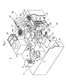
- Fig. 1 is a cutaway perspective view showing an entire semiconductor wafer mounting apparatus in one embodiment of this invention.
- This semiconductor wafer mounting apparatus 1 includes a wafer supplying station 2 for receiving a cassette C storing, in multiple stages, wafers W having undergone a back grinding process, a wafer transport mechanism 3 having a robot arm 4 and a pressing mechanism 5, an alignment stage 7 for performing an aligning operation on each wafer W, an ultraviolet irradiating unit 14 for emitting ultraviolet radiation toward the wafer W placed on the alignment stage 7, a chuck table 15 for holding the wafer W by suction, a ring frame supplying unit 16 storing ring-shaped frames (hereinafter simply called "ring frames f") in multiple stages, a ring frame transport mechanism 17 for transferring each ring frame f to a dicing tape DT, a tape processor 18 for applying the dicing tape DT to the back surface of each ring frame f, a ring frame lift mechanism 26 for vertically moving the ring frame f with the dicing tape DT applied thereto, a mount frame preparing unit 27 for preparing a mount frame MF with the wafer
- the wafer supplying station 2 has a cassette table, and this cassette table receives the cassette C storing, in multiple stages, wafers W having undergone a back grinding process, and having the protective tape applied to patterned surfaces (hereinafter called "front surfaces" as appropriate) thereof. At this time, the wafers W are maintained in horizontal posture with the patterned surfaces facing up.
- the wafer transport mechanism 3 is turned and vertically moved by a drive mechanism not shown. That is, a wafer holder of robot arm 4 and a pressing plate 6 of pressing mechanism 5 to be described hereinafter are positionally adjusted, and each wafer W is transported from the cassette C to the alignment stage 7.
- the robot arm 4 of wafer transport mechanism 3 includes a horseshoe-shaped wafer holder, not shown, attached to a distal end thereof.
- the robot arm 4 is constructed to have the wafer holder movable into and out of spaces between the wafers W stored in multiple stages in the cassette C.
- the wafer holder has suction bores for holding each wafer W at the back surface thereof by vacuum suction.
- the pressing mechanism 5 of wafer transport mechanism 3 includes an arm portion having a circular pressing plate 6 attached to a distal end thereof and substantially corresponding in shape to the wafer W, the arm portion being movable to move the pressing plate 6 over the wafer W placed on the alignment stage 7.
- the shape of pressing plate 6 is not limited to circular, but may be any shape capable of correcting a warp of wafer W. For example, a tip end of a rod-like object may be pressed on a warped portion of wafer W.
- the pressing plate 6 corresponds to the pressing device of this invention.
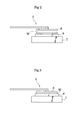
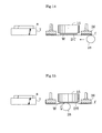
- This pressing mechanism 5 is operable when a faulty suction occurs with the wafer W placed on a support table 8 of alignment stage 7 to be described hereinafter. Specifically, when, as shown in Fig. 2, the wafer W is warped so that the wafer W cannot be held by suction, as shown in Fig. 3, the pressing plate 6 presses the surface of wafer W to correct the warp into a planar state. In this state, the support table 8 holds the back surface of wafer W by vacuum suction.
- the alignment stage 7 has the support table 8 for performing an aligning operation on the wafer W based on an orientation flat, for example, and covering and holding by suction the entire back surface of wafer W.
- this support table 8 has a plurality of suction bores 9 formed therein.
- the respective suction bores 9 communicate with suction paths r which are integrated in upstream positions into one suction pipe R.
- the integrated suction pipe R has a pressure gauge 10, a valve V and a vacuum source 11 arranged in the state order thereon.
- the pressure gauge 10 has a comparator 12 connected thereto for comparing a pressure in time of sucking the wafer W with a predetermined reference value.
- the comparator 12 is connected to a controller 13. When the comparator 12 detects an abnormal pressure variation, this controller 13 receives a detection signal from the comparator 12, and operates the wafer transport mechanism 3 and pressing mechanism 5.
- the pressure gauge 10 and comparator 12 constitute the detecting device of this invention.
- the suction pipe R communicates with the atmosphere through the suction bores 9, and the pressure in the suction pipe R hardly decreases. That is, when the wafer W is placed on the support table 8, the pressure gauge 10 measures the pressure in the suction pipe R.
- the comparator 12 compares a pressure measurement obtained from the pressure gauge 10 and a reference value determined beforehand in relation to a pressure value in time of normal operation (i.e. when the wafer W is normally sucked by the support table 8). When the pressure measurement is higher than the reference value (that is, the pressure in the suction pipe R is not lowered sufficiently), the wafer W is determined to have a warp and not sucked by the support table 8. The comparator 12 sends an abnormal detection signal to the controller 13.
- the controller 13 When this abnormal detection signal is inputted, the controller 13 operates the wafer transport mechanism 3 and pressing mechanism 5 to move the pressing plate 6 over the wafer W as shown in Fig. 2 and lower it as shown in Fig. 3. As a result, the wafer W is pressed to have the warp corrected, whereby the wafer W is sucked by the support table 8.
- the alignment stage 7 is movable, transporting the wafer W as held by suction, between an initial position for supporting and aligning the wafer W, and a position between the chuck table 15 and ring frame lift mechanism 26 arranged in multiple stages above the tape processor 18 to be described hereinafter. That is, the alignment stage 7 transports the wafer W with a warp corrected and maintained in a planar state to the next step.
- the alignment stage 7 corresponds to the transporting device and the aligner of this invention.
- the ultraviolet irradiating unit 14 is disposed above the alignment stage 7 in the initial position.
- the ultraviolet irradiating unit 14 emits ultraviolet radiation toward the protective tape PT which is an ultraviolet curable type adhesive tape applied to the surface of wafer W. That is, the adhesive strength of protective tape PT is reduced by the ultraviolet irradiation.
- the chuck table 15 is circular which is approximately the same shape as the wafer W to cover and hold by vacuum suction the surface of wafer W, and is vertically movable by a drive mechanism not shown from a standby position above the tape processor 18 to a position for applying the wafer W to a ring frame f.
- the chuck table 15 corresponds to the individual holding device and the receiving device of this invention.
- the chuck table 15 contacts and holds by suction the wafer W with a warp corrected and maintained in a planar state by the support table 8.
- the chuck table 15 is movable downward to a position inside an opening of the ring frame lift mechanism 26 holding by suction the ring frame f with the dicing tape DT, to be described hereinafter, applied to the back surface, and adjacent the dicing tape DT at the center of ring frame f.
- the chuck table 15 and ring frame lift mechanism 26 are held by a holding mechanism not shown.
- the ring frame supplying unit 16 has a wagon-like construction with a pulley disposed in a bottom position, and is fitted in a main body of the apparatus 1.
- the frame supplying unit is open at the top through which the ring frames f stored in multiple stages inside are slid upward and fed out.
- the ring frame transport mechanism 17 sucks by vacuum an uppermost one and then a next one of the ring frames f stored in the ring frame supplying unit 16, and successively transports the ring frames f to an alignment stage not shown and to a position for applying the dicing tape DT.
- the ring frame transport mechanism 17 acts also as a holding mechanism, when applying the dicing tape DT, for holding the ring frames f in the position for applying the dicing tape DT.
- the tape processor 18 includes a tape server 19 for supplying the dicing tape DT, a tension mechanism 20 for applying tension to the dicing tape DT, an applicator unit 21 for applying the dicing tape DT to the ring frames f, a cutter mechanism 24 for cutting the dancing tape DT applied to the ring frames f, a separator unit 23 for separating from the ring frames f unwanted tape cut by the cutter mechanism 24, and a tape collector 25 for collecting unwanted tape remaining after the cutting.
- a tape server 19 for supplying the dicing tape DT
- a tension mechanism 20 for applying tension to the dicing tape DT
- an applicator unit 21 for applying the dicing tape DT to the ring frames f
- a cutter mechanism 24 for cutting the dancing tape DT applied to the ring frames f
- a separator unit 23 for separating from the ring frames f unwanted tape cut by the cutter mechanism 24, and a tape collector 25 for collecting unwanted tape remaining after the cutting.
- the tension mechanism 20 holds the dicing tape DT at opposite ends in the direction of width, and applies tension in the direction of width of the tape. That is, where soft dicing tape DT is used, a tension acting in a tape feeding direction results in longitudinal creases formed on the surface of dicing tape DT along the feeding direction. The tension is applied in the direction of width of the tape in order to avoid such creases and apply the dicing tape DT uniformly to the ring frames f.
- the applicator unit 21 is disposed in a standby position obliquely downward (leftward and downward in Fig. 1) of the ring frame f held above the dicing tape DT.
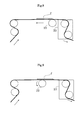
- the applicator unit 21 has an applicator roller 22 which moves to an application starting position rightward in the tape feeding direction shown in Fig. 8, at the same time as the ring frame transport mechanism 17 transports the ring frame f and holds it in the position for applying the dicing tape DT, and the tape server 19 starts feeding the dicing tape DT.
- the applicator roller 22 having arrived at the application starting position moves upward to press and apply the dicing tape DT to the ring frame f and, as shown in Fig. 9, rolls from the application starting position toward a standby position while pressing and applying the dicing tape DT to the ring frame f.
- the separator unit 23 is constructed to separate from the ring frame f unwanted part of the dicing tape DT cut by the cutter mechanism 24 described hereinafter. Specifically, after the dicing tape DT is applied to the ring frame f and cut, the tension mechanism 20 releases the dicing tape DT. Next, as shown in Fig. 10, the separator unit 23 moves on the ring frame f toward the tape server 19 (leftward in Fig. 10) to separate unwanted dicing tape DT after the cutting operation.
- the cutter mechanism 24 is disposed below the dicing tape DT on which the ring frame f is placed. After the dicing tape DT is applied to the ring frame f by the applicator unit 21, the tension mechanism 20 releases the dicing tape DT and the cutter mechanism 24 moves upward. The cutter mechanism 24 having moved upward cuts the dicing tape DT along the ring frame f.
- the ring frame lift mechanism 26 is in a standby position above the position for applying the dicing tape DT to the ring frame f. After the dicing tape DT is applied to the ring frame f, this ring frame lift mechanism 26 descends and holds the ring frame f by suction. At this time, the ring frame transport mechanism 18 which has been holding the ring frame f returns to an initial position above the ring frame supplying unit 16.
- the ring frame lift mechanism 26 holding the ring frame f by suction ascends to a position for joining the wafer W.
- the chuck table 15 holding the wafer W by suction also descends to the position for joining the wafer W.
- the mount frame preparing unit 27 includes an applicator roller 28.
- the applicator roller 28 is arranged to roll while pressing on a non-adhesive surface of the dicing tape DT applied to the back surface of ring frame f.
- the applicator roller 28 is formed of a soft material such as rubber or resin, for example.
- the first mount frame transport mechanism 29 holds by suction the mount frame MF integrating the ring frame f and wafer W, and transfers it to a separating table, not shown, of the separating mechanism 30.
- the separating mechanism 30 includes a separating table (not shown) for receiving and moving the wafer W, a tape server 31 for supplying separator tape Ts, a separator unit 32 for applying and separating the separator tape Ts, and a tape collector 34 for collecting separated separator tape Ts and protective tape PT.
- the construction of separating mechanism 30 except the separating table is arranged on an entire surface of a vertical wall, not shown, of the main body of the apparatus 1.
- the tape server 31 supplies the separator tape Ts drawn from a stock roller to advance over the separating table.
- the separator unit 32 has a separator plate 33.
- This separator plate 33 moves while pressing the surface of protective tape PT applied to the patterned surface of wafer W (wafer W applied to the mount frame MF by means of the dicing tape DT) transported by the separating table.
- the separator plate 33 applies the separator tape Ts to the protective tape PT while pressing on the non-adhesive surface of separator tape Ts, and separates the separator tape Ts and protective tape PT together.
- the separator tape Ts has a width smaller than the diameter of wafer W.
- the second mount frame transport mechanism 35 holds by suction the mount frame MF discharged from the separating mechanism 30, and transfers it to the turntable 36.
- the turntable 36 is constructed to perform an alignment of the mount frame MF and store it in the mount frame collector 37. That is, when the second mount frame transport mechanism 35 places the mount frame MF on the turntable 36, an aligning operation is carried out based on the orientation flat of wafer W and positioning profile of ring frame f.
- the turntable 36 is rotatable to change a direction for storing the mount frame MF in the mount frame collector 37. When a direction for storage is determined, the turntable 36 allows a pusher, not shown, to push out the mount frame MF whereby the mount frame MF is stored in the mount frame collector 37.
- the mount frame collector 37 is placed on a vertically movable support table not shown. Thus, with vertical movement of the support table, the mount frame MF pushed out by the pusher may be stored in a selected stage of mount frame collector 37.
- the wafer holder of robot arm 4 is inserted into a space in the cassette C.
- the wafers W are taken out, one at a time, as held at the lower surface by suction.
- Each wafer W taken out is transported to the alignment stage 7.
- the robot arm 4 places the wafer W on the support table 8 to be held at the back surface by suction.
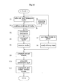
- the pressure gauge 10 detects a suction level of wafer W, and inputs a detection result to the comparator 12.
- the comparator 12 compares this detection result with the reference value determined beforehand in relation to a pressure value in time of normal operation. When the result of comparison shows that the pressure in the suction pipe R has lowered sufficiently, the suction of wafer W is determined to be excellent.
- an aligning operation is performed based on the orientation flat or notch, and the operation proceeds to step S4.
- the pressure measurement is higher than the reference value (that is, the pressure in suction pipe R is not lowered sufficiently)
- the wafer W is determined to have a warp and not sucked by the support table 8. Then, the operation proceeds to step S3.
- the controller 13 transmits signals to the wafer transport mechanism 3 and pressing mechanism 5 for operating each mechanism. That is, the wafer transport mechanism 3 rotates to direct the pressing plate 6 toward the support table 8 and extends the pressing plate 6 over the wafer W as shown in Fig. 2, by way of alignment for pressing the surface of wafer W. After the alignment, the wafer transport mechanism 3 descends to lower the pressing plate 6 to press upon the surface of wafer W as shown in Fig. 3. At the same time, the valve V is opened to have the wafer W held by suction in a planar state with the warp corrected. Further, the wafer W is aligned based on the orientation flat or notch.
- step S2 After the warping of wafer W is corrected by pressurization, the operation returns to step S2 for a confirmation of the sucking of wafer W again.
- the ultraviolet irradiating unit 14 After the alignment on the alignment stage 7, the ultraviolet irradiating unit 14 emits ultraviolet radiation to the surface of wafer W.
- the wafer W is transported as held by suction by the support table 8, and along with the alignment stage 7, to the next mount frame preparing unit 27. That is, the alignment stage 7 moves to the position between the chuck table 15 and ring frame lift mechanism 26.
- the chuck table 15 disposed above descends to have the bottom of chuck table 15 contact and begin sucking the wafer W by vacuum.
- the support table 8 stops its sucking action.
- the wafer W is received by the chuck table 15 in the planar state with the warp corrected.
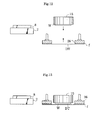
- the alignment stage 7 having released the wafer W returns to the initial position as shown in Fig. 12.
- the ring frame transport mechanism 17 sucks by vacuum and takes out an uppermost one and then a next one of the ring frames f stored in the ring frame supplying unit 16. Each ring frame f taken out is aligned on the alignment stage not shown, and then transported to the position, above the dicing tape DT, for applying the dicing tape DT.
- the tape server 19 starts feeding the dicing tape DT.
- the applicator roller 22 moves to the application starting position.
- the tension mechanism 20 Upon arrival of the applicator roller 22 at the applicator starting position, the tension mechanism 20 holds the dicing tape DT at opposite ends in the direction of width, and applies tension in the direction of width of the tape.
- the applicator roller 22 ascends, and presses to apply the dicing tape DT to an end of the ring frame f.
- the applicator roller 22 rolls toward the standby position adjacent the tape server 19.
- the applicator roller 22 rolls while pressing the dicing tape DT (on the non-adhesive surface thereof), to apply the dicing tape DT to the ring frame f.
- the tension mechanism 20 releases the dicing tape DT.
- the cutter mechanism 24 ascends and cuts the dicing tape DT along the ring frame f. After the dicing tape DT is cut, the separator unit 23 moves toward the tape server 19 to separate unwanted dicing tape DT.
- the tape server 19 operates to draw out the dicing tape DT, and the cut, unwanted part of the tape is sent off to the tape collector 25.
- the applicator roller 22 moves to the application starting position to apply the dicing tape DT to a next ring frame f.
- the ring frame f with the dicing tape DT applied thereto moves upward with the frame portion held by suction by the ring frame lift mechanism 26.
- the chuck table 15 also descends. That is, the chuck table 15 and ring frame lift mechanism 26 both move to the position for applying the wafer W.
- the bottom of chuck table 15 holding the wafer W by suction fits into the opening formed centrally of the ring frame lift mechanism 26.
- the wafer W lies adjacent the adhesive surface of dicing tape DT.
- the applicator roller 28 moves to the position for starting application of the dicing tape DT and, as shown in Fig. 15, rolls while pressing on the non-adhesive surface of dicing tape DT applied to the bottom of ring frame f, to apply the dicing tape DT to the wafer W.
- a mount frame MF is prepared which integrates the ring frame f and wafer W.
- the chuck table 15 and ring frame lift mechanism 26 move upward.
- the support table not shown moves under the mount frame MF, and the mount frame MF is placed on this support table.
- the mount frame MF placed is held by suction by the first mount frame transport mechanism 29 and transferred to the separating table not shown.
- the separating table on which the mount frame MF is placed moves toward a position under the separator unit 32.
- the separator plate 33 presses and applies the separator tape Ts fed from the tape server 31 to the protective tape PT on the surface of wafer W.
- the separator plate 33 while applying the separator tape Ts, separates the applied separator tape Ts along with the protective tape PT from the surface of wafer W.
- the mount frame MF having undergone the process of separating the protective tape PT is moved by the separating table to the standby position of the second mount frame transport mechanism 35.
- the mount frame MF discharged from the separating mechanism 30 is transferred to the turntable 36 by the second mount frame transport mechanism 35.
- the mount frame MF transferred is aligned by means of the orientation flat or notch, together with an adjustment of its direction of storage.
- the mount frame MF is pushed out by the pusher to be stored in the mount frame collector 37.
- the wafer W may reliably be held by the support table 8 by suction.
- the wafer W is transported as held by suction by the support table 8, and along with the alignment stage 7, and the surface of wafer W is placed in contact with the suction surface of chuck table 15.
- the chuck table 15 sucks the wafer W by vacuum, and the support table 8 stops its sucking action.
- the wafer W is transported in a planar state with the warp corrected to a next step. As a result, the wafer W is transported reliably and free of displacement.
- This embodiment is the same as the preceding first embodiment except that the pressing plate 6 of pressing mechanism 5 can hold by suction and transport each wafer W to the alignment stage 7.
- the pressing plate 6 of pressing mechanism 5 can hold by suction and transport each wafer W to the alignment stage 7.
- Like reference numerals are used to identify like parts which will not particularly be described.
- a wafer holder 50 is horseshoe-shaped, and includes two branched distal portions having suction bores 51 for holding by suction a wafer W at the back surface adjacent edges thereof.
- the wafer holder 50 is not limited to the horseshoe shape, but may be ring-shaped or may be a flat plate substantially corresponding in shape to the wafer W, for example. Where the robot arm 4 does not take the wafer W out of the cassette C for transportation, the wafer holder 50 need not have the suction bores 51 for holding the wafer W by suction.
- the pressing mechanism 5 has the pressing plate 6 constructed to be vertically movable and rotatable as well as movable into and out of a space between wafers W stored in multiple stages in the cassette C.
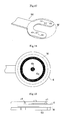
- the pressing plate 6 is capable of holding a wafer W by suction. As shown in Fig. 18, the pressing plate 6 is circular for covering the wafer W. Its surface for contacting the wafer W has an annular groove 6a for holding peripheral regions of wafer W by suction, and a suction bore 6b for holding a central portion of wafer W by suction. As shown in Fig. 21, the annular groove 6a and suction bore 6b are in communication with the vacuum source 11 through a suction path r2 inside the arm and a suction pipe R2.
- the suction holding by the pressing plate 6 is not limited to this form, but may be any form only if capable of reliably holding the wafer W by suction.
- a plurality of suction bores may be arranged equidistantly along the edge of pressing plate 6, or a plurality of suction bores may be arranged radially.
- the annular groove 6a and suction bore 6b correspond to the suction device of this invention.
- the alignment stage 7 has the support table 8 for performing an aligning operation on the wafer W based on an orientation flat, for example, and covering and holding by suction the entire back surface of wafer W.
- the support table 8 has a plurality of suction bores arranged equidistantly along the edge of support table 8 for holding peripheral portions of wafer W by suction.
- the respective suction bores 9 communicate with suction paths r which are integrated in upstream positions into one suction pipe R1.
- the integrated suction pipe R1 has a pressure gauge 10, a valve V and the vacuum source 11 arranged in the state order thereon.
- the pressure gauge 10 has a comparator 12 connected thereto for comparing a pressure in time of sucking the wafer W with a predetermined reference value.
- the comparator 12 is connected to a controller 13. In response to pressure variations obtained from the comparator 12, the controller 13 adjusts the timing of opening and closing the valves V mounted on the suction pipes R1 and R2.
- the pressure gauge 10 and comparator 12 constitute the detecting device of this invention.
- the comparator 12 shown in Fig. 21 compares a pressure measurement obtained from the pressure gauge 10 and a reference value determined beforehand in relation to a pressure value in time of normal operation (i.e. when the wafer W is normally sucked by the support table 8).
- a pressure value in time of normal operation i.e. when the wafer W is normally sucked by the support table 8.
- the pressure measurement is higher than the reference value (that is, the pressure in the suction pipe R1 is not lowered sufficiently)
- the wafer W placed by the pressing plate 6 is determined not being fully sucked by the support table 8.
- the comparator 12 sends to the controller 13 a normal detection signal indicating that the wafer W is sucked fully (normally).
- the valve V mounted on the suction pipe R2 is closed to releases the suction holding of wafer W.
- the alignment stage 7 can receive the wafer W in a planar state with the warp corrected from the pressing plate 6.
- the pressure gauge 10 and comparator unit 12 constitute the detecting device of this invention.
- the wafer holder 50 of robot arm 4 is inserted into a space in the cassette C.
- a wafer W is held by suction from below.
- the pressing plate 6 of pressing mechanism 5 is inserted into a space in the cassette C, that is a space above the wafer W held by the wafer holder 50.
- the pressing plate 6 descends toward wafer W and, as shown in Fig. 19, holds the wafer W by suction while pressing it from above.
- the wafer holder 50 stops its sucking action.
- the pressing plate 6 takes the wafer W out of the cassette C while holding it by suction, and transports it to the alignment stage 7. At this time, the wafer holder 50 moves to a position for taking out a next wafer W.
- the wafer W While being pressed by the pressing plate 6, the wafer W is placed on the support table 8 of alignment stage 7. The support table 8 begins to suck the wafer W. At this time, a suction level of wafer W is successively detected by the pressure gauge 10, and a result of detection is inputted to the comparator 12.
- the comparator 12 compares the detection result with the reference value determined beforehand in relation to a pressure value in time of normal operation. When the result of comparison shows that the pressure in the suction pipe R has lowered sufficiently, the suction of wafer W is determined to be excellent and a normal detection signal is sent to the controller 13.
- the controller 13 Upon receipt of the normal detection signal, the controller 13 closes the valve V mounted on the pipe R2 and cancels the suction holding of the wafer W by the pressing plate 6.
- the pressing plate 6 moves to the cassette C to fetch a next wafer W, or returns to the standby position.
- the alignment stage 7 aligns the wafer W held by suction, based on the orientation flat or notch. After the alignment, the ultraviolet irradiating unit 14 emits ultraviolet radiation to the surface of wafer W.
- the wafer W is transported as held by suction by the support table 8, and along with the alignment stage 7, to the next mount frame preparing unit 27.
- the support table 8 can receive the wafer W as maintained in a planar state by the pressing plate 6. Specifically, the pressing plate 6, while holding by suction and pressing the wafer W, places the wafer W on the support table 8. The support table 8 holds by suction the wafer W in the planar state with the warp corrected. The pressing plate 6 releases the wafer W at a point of time when the support table 8 fully (normally) holds the wafer W by suction. Thus, the support table 8 can reliably hold the wafer W, and the alignment stage 7 also can perform alignment accurately.
- the wafer W is placed on the support table 8 while the pressing plate 6 holds the surface of wafer W by suction from above. Subsequently, the pressing plate 6 ascends to return or move to the standby position. It is therefore unnecessary to design the suction bores in the support table 8 by taking a retraction space for the wafer holder 50 into account as in the case of a conventional apparatus where the wafer W is placed on the support table 8 while the wafer holder 50 remains holding the lower surface of the wafer. That is, the support table 8 and alignment stage 7 may be varied in design for holding the wafer W by suction.
Landscapes
- Container, Conveyance, Adherence, Positioning, Of Wafer (AREA)
Abstract
Description
Claims (23)
- A semiconductor wafer transport method for transporting a semiconductor wafer, said method comprising:a supporting step for supporting said semiconductor wafer in a planar state with a warp thereof corrected; anda transporting step for transporting said semiconductor wafer supported in the planar state.
- A semiconductor wafer transport method as defined in claim 1, wherein said supporting step is a step of pressing on a surface of said semiconductor wafer, and holding said semiconductor wafer in the planar state by suction.
- A semiconductor wafer transport method as defined in claim 1, further comprising an aligning step for aligning said semiconductor wafer with the warp corrected in said supporting step.
- A semiconductor wafer transport method as defined in claim 3, wherein, in said aligning step, the semiconductor wafer is aligned by an aligner, with the warp corrected by a pressure imparted by a pressing device.
- A semiconductor wafer transport method as defined in claim 4, wherein, in said aligning step, the semiconductor wafer is aligned by the aligner, with the warp corrected by the pressure imparted by the pressing device, and the pressing device releases the semiconductor wafer when the aligner holds the semiconductor wafer by suction.
- A semiconductor wafer transport method as defined in claim 3, wherein the semiconductor wafer, while being maintained in the planar state with the warp corrected in said supporting step, has a surface thereof irradiated with ultraviolet radiation.
- A semiconductor wafer transport method as defined in claim 1, further comprising a receiving step for causing an individual holding device to contact the semiconductor wafer transported in said planar state, and receiving the semiconductor wafer held by said holding device by suction.
- A semiconductor wafer transport method as defined in claim 7, wherein the semiconductor wafer maintained in the planar state is transported by moving the aligner.
- A semiconductor wafer transport method as defined in claim 1, further comprising a step of pressing, with a pressing device, the semiconductor wafer held by a robot arm, and sucking, receiving and transporting the semiconductor wafer in a warp-corrected state.
- A semiconductor wafer transport method as defined in claim 9, wherein the semiconductor wafer transported by the said robot arm is received by the pressing device.
- A semiconductor wafer transport method as defined in claim 9, wherein the semiconductor wafer is received by the pressing device from the robot arm holding the semiconductor wafer in a cassette storing said semiconductor wafers in multiple stages.
- A semiconductor wafer transport method as defined in claim 1, further comprising a step of transporting said semiconductor wafer sandwiched between a robot arm for holding the semiconductor wafer and a pressing device for pressing the semiconductor wafer.
- A semiconductor wafer transport method as defined in claim 1, further comprising a step of transporting the semiconductor wafer as held by suction with the warp corrected by pressing the semiconductor wafer with a pressing device.
- A semiconductor wafer transport method as defined in claim 13, wherein said semiconductor wafer is transported between different processing apparatus as held by suction by the pressing device.
- A semiconductor wafer transport method as defined in claim 1, wherein said semiconductor wafer is held by suction as pressed at least at peripheral portions and a central portion thereof.
- A semiconductor wafer transport method as defined in claim 1, wherein said semiconductor wafer has a protective tape applied to a surface thereof beforehand.
- A semiconductor wafer transport apparatus for transporting a semiconductor wafer, said apparatus comprising:a support table for supporting and holding by suction said semiconductor wafer;a pressing device for pressing on a surface of the semiconductor wafer supported on said support table; anda transporting device for transporting the semiconductor wafer pressed and held by suction by said support table.
- A semiconductor wafer transport apparatus as defined in claim 17, further comprising a receiving device for contacting the semiconductor wafer transported by said transporting device, and receiving the semiconductor wafer while holding the semiconductor wafer by suction.
- A semiconductor wafer transport apparatus as defined in claim 17, further comprising a detecting device for detecting a warp of the semiconductor wafer placed on said support table.
- A semiconductor wafer transport apparatus as defined in claim 17, wherein said transporting device is an aligner for aligning the semiconductor wafer.
- A semiconductor wafer transport apparatus as defined in claim 17, wherein said pressing device is a suction device for holding the semiconductor wafer by suction.
- A semiconductor wafer transport apparatus as defined in claim 17, further comprising a robot arm for taking, or taking and transporting, the semiconductor wafer from a cassette storing semiconductor wafers in multiple stages.
- A semiconductor wafer transport apparatus as defined in claim 22, further comprising a control device operable, when the semiconductor wafer is transferred from said pressing device to the aligner, for controlling release of the semiconductor wafer by the pressing device, and timing of the aligner holding the semiconductor wafer by suction.
Applications Claiming Priority (4)
| Application Number | Priority Date | Filing Date | Title |
|---|---|---|---|
| JP2001368629 | 2001-12-03 | ||
| JP2001368629 | 2001-12-03 | ||
| JP2002292568A JP4201564B2 (en) | 2001-12-03 | 2002-10-04 | Semiconductor wafer transfer method and semiconductor wafer transfer apparatus using the same |
| JP2002292568 | 2002-10-04 |
Publications (3)
| Publication Number | Publication Date |
|---|---|
| EP1320121A2 true EP1320121A2 (en) | 2003-06-18 |
| EP1320121A3 EP1320121A3 (en) | 2006-07-05 |
| EP1320121B1 EP1320121B1 (en) | 2010-02-17 |
Family
ID=26624840
Family Applications (1)
| Application Number | Title | Priority Date | Filing Date |
|---|---|---|---|
| EP02026785A Expired - Lifetime EP1320121B1 (en) | 2001-12-03 | 2002-12-02 | Semiconductor wafer transport method and apparatus |
Country Status (9)
| Country | Link |
|---|---|
| US (1) | US7078262B2 (en) |
| EP (1) | EP1320121B1 (en) |
| JP (1) | JP4201564B2 (en) |
| KR (1) | KR100901040B1 (en) |
| CN (1) | CN100390953C (en) |
| AT (1) | ATE458267T1 (en) |
| DE (1) | DE60235343D1 (en) |
| SG (1) | SG111979A1 (en) |
| TW (1) | TWI251893B (en) |
Cited By (5)
| Publication number | Priority date | Publication date | Assignee | Title |
|---|---|---|---|---|
| GB2395841A (en) * | 2002-10-24 | 2004-06-02 | Lintec Corp | Aligning thinned semiconductor wafers |
| FR2857504A1 (en) * | 2003-07-08 | 2005-01-14 | Atmel Grenoble Sa | LARGE IMAGE SENSOR AND METHOD OF MANUFACTURE |
| EP1912250A1 (en) | 2006-09-07 | 2008-04-16 | Nitto Denko Corporation | Adhesive tape cutting method and tape cutting apparatus |
| EP1672684A4 (en) * | 2003-10-10 | 2010-05-26 | Lintec Corp | DEVICE AND METHOD FOR MOUNTING |
| EP2851941A1 (en) * | 2013-09-23 | 2015-03-25 | Mechatronic Systemtechnik GmbH | Method for transferring a thinned, in particular ground, semiconductor wafer |
Families Citing this family (71)
| Publication number | Priority date | Publication date | Assignee | Title |
|---|---|---|---|---|
| US20060194412A1 (en) * | 2004-04-07 | 2006-08-31 | Takehito Nakayama | Method and device for sticking tape |
| JP4647197B2 (en) * | 2003-09-17 | 2011-03-09 | 東京エレクトロン株式会社 | Method of transporting workpiece and computer-readable storage medium |
| US8359895B2 (en) * | 2003-10-15 | 2013-01-29 | Modern Body Engineering Corporation | Machine cell with vacuum nest for holding a metal panel during a forming operation |
| JP2005150177A (en) * | 2003-11-12 | 2005-06-09 | Nitto Denko Corp | Adhesive tape application method and adhesive tape application device on backside of semiconductor wafer |
| JP4489414B2 (en) * | 2003-11-26 | 2010-06-23 | 株式会社 日立ディスプレイズ | Display device manufacturing method and manufacturing apparatus thereof |
| US7074695B2 (en) * | 2004-03-02 | 2006-07-11 | Chippac, Inc. | DBG system and method with adhesive layer severing |
| TW200539357A (en) * | 2004-04-28 | 2005-12-01 | Lintec Corp | Adhering apparatus and adhering method |
| JP4704756B2 (en) * | 2005-01-04 | 2011-06-22 | オリンパス株式会社 | Substrate transfer device |
| US20070033827A1 (en) * | 2005-07-28 | 2007-02-15 | Kim Young M | Apparatus for moving up and down a wafer cassette and chip sorter having the apparatus |
| JP4461176B2 (en) * | 2005-08-11 | 2010-05-12 | リンテック株式会社 | Sheet sticking device and sticking method |
| JP4611180B2 (en) * | 2005-11-18 | 2011-01-12 | 日東電工株式会社 | Error display device |
| JP2007214357A (en) * | 2006-02-09 | 2007-08-23 | Nitto Denko Corp | Work sticking support method and work sticking support apparatus using the same |
| JP4781901B2 (en) * | 2006-05-08 | 2011-09-28 | 東京エレクトロン株式会社 | Heat treatment method, program and heat treatment apparatus |
| JP4693696B2 (en) * | 2006-06-05 | 2011-06-01 | 株式会社東京精密 | Work processing device |
| JP4698519B2 (en) * | 2006-07-31 | 2011-06-08 | 日東電工株式会社 | Semiconductor wafer mount equipment |
| JP4841355B2 (en) | 2006-08-08 | 2011-12-21 | 日東電工株式会社 | Method for holding semiconductor wafer |
| JP4974626B2 (en) * | 2006-09-20 | 2012-07-11 | 日東電工株式会社 | Adhesive tape cutting method and adhesive tape attaching apparatus using the same |
| JP4974639B2 (en) * | 2006-10-20 | 2012-07-11 | 日東電工株式会社 | Adhesive tape cutting method and apparatus using the same |
| JP4745945B2 (en) * | 2006-12-04 | 2011-08-10 | リンテック株式会社 | Conveying device, sheet sticking device using the same, and sheet peeling device |
| JP4661807B2 (en) * | 2007-03-13 | 2011-03-30 | パナソニック株式会社 | Component mounting apparatus and board conveying method |
| JP4661808B2 (en) * | 2007-03-14 | 2011-03-30 | パナソニック株式会社 | Component mounting apparatus and board conveying method |
| JP4853872B2 (en) * | 2007-05-24 | 2012-01-11 | ラピスセミコンダクタ株式会社 | Chip manufacturing method |
| JP4856593B2 (en) * | 2007-07-04 | 2012-01-18 | リンテック株式会社 | MOUNTING DEVICE AND MOUNTING METHOD |
| JP2008177600A (en) * | 2008-03-26 | 2008-07-31 | Nitto Denko Corp | Adhesive tape application method and adhesive tape application device on backside of semiconductor wafer |
| JP5015848B2 (en) * | 2008-04-08 | 2012-08-29 | リンテック株式会社 | Alignment device |
| DE102008018536B4 (en) * | 2008-04-12 | 2020-08-13 | Erich Thallner | Device and method for applying and / or detaching a wafer to / from a carrier |
| NL1036785A1 (en) * | 2008-04-18 | 2009-10-20 | Asml Netherlands Bv | Rapid exchange device for lithography reticles. |
| SG142402A1 (en) * | 2008-05-02 | 2009-11-26 | Rokko Ventures Pte Ltd | Apparatus and method for multiple substrate processing |
| US8145349B2 (en) * | 2008-05-14 | 2012-03-27 | Formfactor, Inc. | Pre-aligner search |
| JP5216472B2 (en) * | 2008-08-12 | 2013-06-19 | 日東電工株式会社 | Method and apparatus for attaching protective tape to semiconductor wafer |
| US9343273B2 (en) * | 2008-09-25 | 2016-05-17 | Seagate Technology Llc | Substrate holders for uniform reactive sputtering |
| JP5180801B2 (en) * | 2008-12-17 | 2013-04-10 | リンテック株式会社 | Alignment apparatus and alignment method |
| JP5554013B2 (en) * | 2009-05-15 | 2014-07-23 | リンテック株式会社 | Conveying apparatus and conveying method for plate member |
| JP5324319B2 (en) * | 2009-05-26 | 2013-10-23 | 日東電工株式会社 | Wafer mounting method and wafer mounting apparatus |
| CN102004293B (en) * | 2009-09-02 | 2014-04-23 | 鸿富锦精密工业(深圳)有限公司 | Optical element picking and placing device and method for picking and placing multiple optical elements |
| JP5585379B2 (en) * | 2010-10-21 | 2014-09-10 | 富士電機株式会社 | Semiconductor device manufacturing method and manufacturing apparatus thereof |
| US8496159B2 (en) * | 2011-06-06 | 2013-07-30 | International Business Machines Corporation | Injection molded solder process for forming solder bumps on substrates |
| JP5977042B2 (en) * | 2012-02-27 | 2016-08-24 | 株式会社Screenホールディングス | Coating device, substrate holding device, and substrate holding method |
| KR102110000B1 (en) * | 2012-08-31 | 2020-05-12 | 세미컨덕터 테크놀로지스 앤드 인스트루먼츠 피티이 엘티디 | Single ultra-planar wafer table structure for both wafers and film frames |
| TWI571949B (en) * | 2013-01-10 | 2017-02-21 | 晶元光電股份有限公司 | Semiconductor component turning device |
| JP6122299B2 (en) | 2013-01-15 | 2017-04-26 | キヤノン株式会社 | Processing apparatus, processing method, and device manufacturing method |
| JP2014150206A (en) * | 2013-02-04 | 2014-08-21 | Disco Abrasive Syst Ltd | Conveyance device of plate-like material |
| JP6087669B2 (en) | 2013-03-06 | 2017-03-01 | キヤノン株式会社 | Substrate processing apparatus, lithographic apparatus, and article manufacturing method |
| US9355882B2 (en) * | 2013-12-04 | 2016-05-31 | Taiwan Semiconductor Manufacturing Co., Ltd. | Transfer module for bowed wafers |
| JP6253089B2 (en) * | 2013-12-10 | 2017-12-27 | 株式会社ディスコ | Grinding equipment |
| CN103779453B (en) * | 2014-01-21 | 2016-09-14 | 中国科学院半导体研究所 | A kind of device controlling semiconductor LED epitaxial wafer internal stress |
| JP6300629B2 (en) * | 2014-05-13 | 2018-03-28 | 株式会社ディスコ | Load measuring device |
| JP6373068B2 (en) * | 2014-05-30 | 2018-08-15 | 株式会社ディスコ | Transport method |
| TWI581904B (en) * | 2014-11-18 | 2017-05-11 | 漢民科技股份有限公司 | Workpiece processing device and method |
| JP6474275B2 (en) * | 2015-02-19 | 2019-02-27 | 株式会社ディスコ | Processing equipment |
| JP6568781B2 (en) * | 2015-04-04 | 2019-08-28 | 東京エレクトロン株式会社 | Substrate holding method, substrate holding apparatus, processing method and processing apparatus |
| JP6709726B2 (en) * | 2015-12-18 | 2020-06-17 | 日本特殊陶業株式会社 | Substrate holding device, substrate holding member, and substrate holding method |
| KR101812209B1 (en) * | 2016-02-16 | 2017-12-26 | 주식회사 이오테크닉스 | Laser marking apparatus and laser marking method |
| JP6723131B2 (en) | 2016-09-29 | 2020-07-15 | 株式会社Screenホールディングス | Substrate transfer device and substrate transfer method |
| JP6990038B2 (en) * | 2017-04-26 | 2022-01-12 | 日東電工株式会社 | Board detachment method and substrate detachment device |
| JP6978877B2 (en) * | 2017-09-04 | 2021-12-08 | キヤノン株式会社 | Imprint device and article manufacturing method |
| EP3813100B1 (en) | 2018-06-22 | 2026-05-06 | Rorze Corporation | Aligner and correction value calculation method for aligner |
| JP7303635B2 (en) * | 2019-01-07 | 2023-07-05 | 株式会社ディスコ | Work holding method and work processing method |
| JP7161415B2 (en) * | 2019-01-21 | 2022-10-26 | 株式会社ディスコ | processing equipment |
| US11177146B2 (en) | 2019-10-31 | 2021-11-16 | Applied Materials, Inc. | Methods and apparatus for processing a substrate |
| KR102933588B1 (en) * | 2020-07-14 | 2026-03-04 | 삼성전자주식회사 | Wafer to wafer bonding apparatus and wafer to wafer bonding method |
| JP7464472B2 (en) * | 2020-07-17 | 2024-04-09 | 株式会社ディスコ | Processing Equipment |
| KR102417320B1 (en) | 2020-08-26 | 2022-07-06 | 주식회사 쿠온솔루션 | Transfer apparatus for transferring floated object |
| JP7517936B2 (en) * | 2020-10-01 | 2024-07-17 | 株式会社ディスコ | Processing Equipment |
| JP7354084B2 (en) * | 2020-11-17 | 2023-10-02 | Towa株式会社 | Laser processing equipment and method for manufacturing processed products |
| WO2022118468A1 (en) * | 2020-12-04 | 2022-06-09 | 日本電信電話株式会社 | Substrate for wafer conveyance |
| KR20220111067A (en) * | 2021-02-01 | 2022-08-09 | 주식회사 야스 | Evaporation system |
| JP7678083B2 (en) * | 2021-03-18 | 2025-05-15 | Towa株式会社 | Processing device and manufacturing method of processed products |
| JP7482825B2 (en) * | 2021-04-19 | 2024-05-14 | 三菱電機株式会社 | Inspection device, semiconductor substrate inspection method, semiconductor substrate manufacturing method, and semiconductor device manufacturing method |
| JP7730666B2 (en) * | 2021-06-01 | 2025-08-28 | 株式会社ディスコ | Processing method and processing device |
| TWI773378B (en) * | 2021-06-11 | 2022-08-01 | 亞亞科技股份有限公司 | Pick-and-place and pressing module of circuit board inspection device |
Family Cites Families (29)
| Publication number | Priority date | Publication date | Assignee | Title |
|---|---|---|---|---|
| DE3110341C2 (en) * | 1980-03-19 | 1983-11-17 | Hitachi, Ltd., Tokyo | Method and apparatus for aligning a thin substrate in the image plane of a copier |
| JPS59134848A (en) * | 1983-01-22 | 1984-08-02 | Nec Corp | wafer chuck |
| JPS61276339A (en) * | 1985-05-31 | 1986-12-06 | Nec Corp | Wafer stage |
| JPH0697676B2 (en) * | 1985-11-26 | 1994-11-30 | 忠弘 大見 | Wafer susceptor device |
| US4962441A (en) * | 1989-04-10 | 1990-10-09 | Applied Materials, Inc. | Isolated electrostatic wafer blade clamp |
| JPH0499320A (en) * | 1990-08-17 | 1992-03-31 | Soatetsuku:Kk | Automatic centering method for wafer protective tape |
| USH1373H (en) * | 1992-04-06 | 1994-11-01 | American Telephone And Telegraph Company | Wafer handling apparatus and method |
| JPH05315434A (en) * | 1992-05-07 | 1993-11-26 | Nec Yamagata Ltd | Semiconductor wafer retainer |
| JPH0758191A (en) * | 1993-08-13 | 1995-03-03 | Toshiba Corp | Wafer stage device |
| US5515167A (en) * | 1994-09-13 | 1996-05-07 | Hughes Aircraft Company | Transparent optical chuck incorporating optical monitoring |
| US5622400A (en) * | 1995-06-07 | 1997-04-22 | Karl Suss America, Inc. | Apparatus and method for handling semiconductor wafers |
| US5759006A (en) * | 1995-07-27 | 1998-06-02 | Nitto Denko Corporation | Semiconductor wafer loading and unloading apparatus, and semiconductor wafer transport containers for use therewith |
| US5703493A (en) * | 1995-10-25 | 1997-12-30 | Motorola, Inc. | Wafer holder for semiconductor applications |
| JP3586817B2 (en) * | 1995-12-26 | 2004-11-10 | 株式会社オーク製作所 | Image forming exposure apparatus and work positioning method |
| US5930652A (en) * | 1996-05-28 | 1999-07-27 | Motorola, Inc. | Semiconductor encapsulation method |
| JPH1092776A (en) * | 1996-09-12 | 1998-04-10 | Disco Abrasive Syst Ltd | Workpiece protection member and wafer polishing method |
| JPH10154671A (en) * | 1996-11-26 | 1998-06-09 | Mitsubishi Electric Corp | Semiconductor manufacturing apparatus and semiconductor device manufacturing method |
| US5861632A (en) * | 1997-08-05 | 1999-01-19 | Advanced Micro Devices, Inc. | Method for monitoring the performance of an ion implanter using reusable wafers |
| JPH1174164A (en) * | 1997-08-27 | 1999-03-16 | Canon Inc | Substrate processing apparatus, substrate support apparatus, substrate processing method, and substrate manufacturing method |
| JPH11176731A (en) * | 1997-12-15 | 1999-07-02 | Nitto Denko Corp | Resist removal equipment |
| JP4283926B2 (en) * | 1999-02-22 | 2009-06-24 | 株式会社アルバック | Wafer cassette wafer holding system |
| EP1089328A1 (en) * | 1999-09-29 | 2001-04-04 | Infineon Technologies AG | Method for manufacturing of a semiconductor device |
| JP4085538B2 (en) * | 1999-10-15 | 2008-05-14 | ソニー株式会社 | Inspection device |
| US6431769B1 (en) * | 1999-10-25 | 2002-08-13 | Tokyo Electron Limited | Substrate processing system and substrate processing method |
| JP2001239487A (en) * | 2000-02-29 | 2001-09-04 | Nippei Toyama Corp | Vacuum holding device and vacuum holding release method in wafer transfer device |
| JP4302284B2 (en) * | 2000-03-29 | 2009-07-22 | リンテック株式会社 | Semiconductor wafer transfer equipment |
| US6541989B1 (en) * | 2000-09-29 | 2003-04-01 | Motorola, Inc. | Testing device for semiconductor components and a method of using the device |
| US6612590B2 (en) * | 2001-01-12 | 2003-09-02 | Tokyo Electron Limited | Apparatus and methods for manipulating semiconductor wafers |
| JP3983053B2 (en) * | 2002-01-17 | 2007-09-26 | 日東電工株式会社 | Protective tape cutting method and protective tape applying apparatus using the same |
-
2002
- 2002-10-04 JP JP2002292568A patent/JP4201564B2/en not_active Expired - Fee Related
- 2002-11-26 US US10/303,816 patent/US7078262B2/en not_active Expired - Fee Related
- 2002-11-28 SG SG200207203A patent/SG111979A1/en unknown
- 2002-11-29 KR KR1020020075190A patent/KR100901040B1/en not_active Expired - Fee Related
- 2002-12-02 AT AT02026785T patent/ATE458267T1/en active
- 2002-12-02 TW TW091134903A patent/TWI251893B/en not_active IP Right Cessation
- 2002-12-02 DE DE60235343T patent/DE60235343D1/en not_active Expired - Lifetime
- 2002-12-02 EP EP02026785A patent/EP1320121B1/en not_active Expired - Lifetime
- 2002-12-03 CN CNB021557950A patent/CN100390953C/en not_active Expired - Fee Related
Cited By (8)
| Publication number | Priority date | Publication date | Assignee | Title |
|---|---|---|---|---|
| GB2395841A (en) * | 2002-10-24 | 2004-06-02 | Lintec Corp | Aligning thinned semiconductor wafers |
| GB2395841B (en) * | 2002-10-24 | 2006-01-04 | Lintec Corp | Alignment apparatus |
| US7274452B2 (en) | 2002-10-24 | 2007-09-25 | Lintec Corporation | Alignment apparatus |
| FR2857504A1 (en) * | 2003-07-08 | 2005-01-14 | Atmel Grenoble Sa | LARGE IMAGE SENSOR AND METHOD OF MANUFACTURE |
| EP1672684A4 (en) * | 2003-10-10 | 2010-05-26 | Lintec Corp | DEVICE AND METHOD FOR MOUNTING |
| US8196632B2 (en) | 2003-10-10 | 2012-06-12 | Lintec Corporation | Mounting apparatus and mounting method |
| EP1912250A1 (en) | 2006-09-07 | 2008-04-16 | Nitto Denko Corporation | Adhesive tape cutting method and tape cutting apparatus |
| EP2851941A1 (en) * | 2013-09-23 | 2015-03-25 | Mechatronic Systemtechnik GmbH | Method for transferring a thinned, in particular ground, semiconductor wafer |
Also Published As
| Publication number | Publication date |
|---|---|
| EP1320121A3 (en) | 2006-07-05 |
| KR20030045602A (en) | 2003-06-11 |
| DE60235343D1 (en) | 2010-04-01 |
| TWI251893B (en) | 2006-03-21 |
| ATE458267T1 (en) | 2010-03-15 |
| US7078262B2 (en) | 2006-07-18 |
| TW200300999A (en) | 2003-06-16 |
| CN1422791A (en) | 2003-06-11 |
| SG111979A1 (en) | 2005-06-29 |
| KR100901040B1 (en) | 2009-06-04 |
| CN100390953C (en) | 2008-05-28 |
| JP2003234392A (en) | 2003-08-22 |
| EP1320121B1 (en) | 2010-02-17 |
| JP4201564B2 (en) | 2008-12-24 |
| US20030133762A1 (en) | 2003-07-17 |
Similar Documents
| Publication | Publication Date | Title |
|---|---|---|
| US7078262B2 (en) | Semiconductor wafer transport method and semiconductor wafer transport apparatus using the same | |
| US7987888B2 (en) | Releasing method and releasing apparatus of work having adhesive tape | |
| US8097121B2 (en) | Protective tape separation method and protective tape separation apparatus | |
| US7849900B2 (en) | Apparatus for joining a separating adhesive tape | |
| JP5324319B2 (en) | Wafer mounting method and wafer mounting apparatus | |
| TWI693666B (en) | Method and apparatus for mounting semiconductor wafer | |
| JP4995796B2 (en) | Adhesive tape application method and adhesive tape application device | |
| JP4918539B2 (en) | Protective tape peeling device | |
| CN100459091C (en) | Method and apparatus for attaching adhesive tape to backside of semiconductor wafer | |
| EP1912250B1 (en) | Adhesive tape cutting method and tape cutting apparatus | |
| JP4407933B2 (en) | Adhesive tape attaching method and apparatus using the same | |
| KR101948940B1 (en) | Method for separating protective tape and apparatus for separating protective tape | |
| JP4549172B2 (en) | Wafer mounting method and wafer mounting apparatus using the same | |
| JP4295271B2 (en) | Protective tape peeling method and apparatus using the same | |
| JP6653032B2 (en) | Semiconductor wafer mounting method and semiconductor wafer mounting apparatus | |
| JP2023089631A (en) | Protective member forming device | |
| CN116895551A (en) | layered devices |
Legal Events
| Date | Code | Title | Description |
|---|---|---|---|
| PUAI | Public reference made under article 153(3) epc to a published international application that has entered the european phase |
Free format text: ORIGINAL CODE: 0009012 |
|
| AK | Designated contracting states |
Designated state(s): AT BE BG CH CY CZ DE DK EE ES FI FR GB GR IE IT LI LU MC NL PT SE SI SK TR |
|
| AX | Request for extension of the european patent |
Extension state: AL LT LV MK RO |
|
| PUAL | Search report despatched |
Free format text: ORIGINAL CODE: 0009013 |
|
| AK | Designated contracting states |
Kind code of ref document: A3 Designated state(s): AT BE BG CH CY CZ DE DK EE ES FI FR GB GR IE IT LI LU MC NL PT SE SI SK TR |
|
| AX | Request for extension of the european patent |
Extension state: AL LT LV MK RO |
|
| 17P | Request for examination filed |
Effective date: 20061010 |
|
| 17Q | First examination report despatched |
Effective date: 20061206 |
|
| AKX | Designation fees paid |
Designated state(s): AT BE BG CH CY CZ DE DK EE ES FI FR GB GR IE IT LI LU MC NL PT SE SI SK TR |
|
| GRAP | Despatch of communication of intention to grant a patent |
Free format text: ORIGINAL CODE: EPIDOSNIGR1 |
|
| GRAS | Grant fee paid |
Free format text: ORIGINAL CODE: EPIDOSNIGR3 |
|
| GRAA | (expected) grant |
Free format text: ORIGINAL CODE: 0009210 |
|
| AK | Designated contracting states |
Kind code of ref document: B1 Designated state(s): AT BE BG CH CY CZ DE DK EE ES FI FR GB GR IE IT LI LU MC NL PT SE SI SK TR |
|
| REG | Reference to a national code |
Ref country code: GB Ref legal event code: FG4D |
|
| REG | Reference to a national code |
Ref country code: CH Ref legal event code: EP |
|
| REG | Reference to a national code |
Ref country code: IE Ref legal event code: FG4D |
|
| REF | Corresponds to: |
Ref document number: 60235343 Country of ref document: DE Date of ref document: 20100401 Kind code of ref document: P |
|
| REG | Reference to a national code |
Ref country code: NL Ref legal event code: VDEP Effective date: 20100217 |
|
| PG25 | Lapsed in a contracting state [announced via postgrant information from national office to epo] |
Ref country code: ES Free format text: LAPSE BECAUSE OF FAILURE TO SUBMIT A TRANSLATION OF THE DESCRIPTION OR TO PAY THE FEE WITHIN THE PRESCRIBED TIME-LIMIT Effective date: 20100528 Ref country code: PT Free format text: LAPSE BECAUSE OF FAILURE TO SUBMIT A TRANSLATION OF THE DESCRIPTION OR TO PAY THE FEE WITHIN THE PRESCRIBED TIME-LIMIT Effective date: 20100617 |
|
| PG25 | Lapsed in a contracting state [announced via postgrant information from national office to epo] |
Ref country code: SI Free format text: LAPSE BECAUSE OF FAILURE TO SUBMIT A TRANSLATION OF THE DESCRIPTION OR TO PAY THE FEE WITHIN THE PRESCRIBED TIME-LIMIT Effective date: 20100217 Ref country code: FI Free format text: LAPSE BECAUSE OF FAILURE TO SUBMIT A TRANSLATION OF THE DESCRIPTION OR TO PAY THE FEE WITHIN THE PRESCRIBED TIME-LIMIT Effective date: 20100217 |
|
| PG25 | Lapsed in a contracting state [announced via postgrant information from national office to epo] |
Ref country code: EE Free format text: LAPSE BECAUSE OF FAILURE TO SUBMIT A TRANSLATION OF THE DESCRIPTION OR TO PAY THE FEE WITHIN THE PRESCRIBED TIME-LIMIT Effective date: 20100217 Ref country code: GR Free format text: LAPSE BECAUSE OF FAILURE TO SUBMIT A TRANSLATION OF THE DESCRIPTION OR TO PAY THE FEE WITHIN THE PRESCRIBED TIME-LIMIT Effective date: 20100518 Ref country code: NL Free format text: LAPSE BECAUSE OF FAILURE TO SUBMIT A TRANSLATION OF THE DESCRIPTION OR TO PAY THE FEE WITHIN THE PRESCRIBED TIME-LIMIT Effective date: 20100217 Ref country code: SE Free format text: LAPSE BECAUSE OF FAILURE TO SUBMIT A TRANSLATION OF THE DESCRIPTION OR TO PAY THE FEE WITHIN THE PRESCRIBED TIME-LIMIT Effective date: 20100217 Ref country code: CY Free format text: LAPSE BECAUSE OF FAILURE TO SUBMIT A TRANSLATION OF THE DESCRIPTION OR TO PAY THE FEE WITHIN THE PRESCRIBED TIME-LIMIT Effective date: 20100217 |
|
| PG25 | Lapsed in a contracting state [announced via postgrant information from national office to epo] |
Ref country code: CZ Free format text: LAPSE BECAUSE OF FAILURE TO SUBMIT A TRANSLATION OF THE DESCRIPTION OR TO PAY THE FEE WITHIN THE PRESCRIBED TIME-LIMIT Effective date: 20100217 Ref country code: BG Free format text: LAPSE BECAUSE OF FAILURE TO SUBMIT A TRANSLATION OF THE DESCRIPTION OR TO PAY THE FEE WITHIN THE PRESCRIBED TIME-LIMIT Effective date: 20100517 Ref country code: SK Free format text: LAPSE BECAUSE OF FAILURE TO SUBMIT A TRANSLATION OF THE DESCRIPTION OR TO PAY THE FEE WITHIN THE PRESCRIBED TIME-LIMIT Effective date: 20100217 |
|
| PLBE | No opposition filed within time limit |
Free format text: ORIGINAL CODE: 0009261 |
|
| STAA | Information on the status of an ep patent application or granted ep patent |
Free format text: STATUS: NO OPPOSITION FILED WITHIN TIME LIMIT |
|
| 26N | No opposition filed |
Effective date: 20101118 |
|
| PG25 | Lapsed in a contracting state [announced via postgrant information from national office to epo] |
Ref country code: DK Free format text: LAPSE BECAUSE OF FAILURE TO SUBMIT A TRANSLATION OF THE DESCRIPTION OR TO PAY THE FEE WITHIN THE PRESCRIBED TIME-LIMIT Effective date: 20100217 |
|
| PG25 | Lapsed in a contracting state [announced via postgrant information from national office to epo] |
Ref country code: IT Free format text: LAPSE BECAUSE OF FAILURE TO SUBMIT A TRANSLATION OF THE DESCRIPTION OR TO PAY THE FEE WITHIN THE PRESCRIBED TIME-LIMIT Effective date: 20100217 |
|
| PG25 | Lapsed in a contracting state [announced via postgrant information from national office to epo] |
Ref country code: MC Free format text: LAPSE BECAUSE OF NON-PAYMENT OF DUE FEES Effective date: 20101231 |
|
| REG | Reference to a national code |
Ref country code: CH Ref legal event code: PL |
|
| GBPC | Gb: european patent ceased through non-payment of renewal fee |
Effective date: 20101202 |
|
| REG | Reference to a national code |
Ref country code: FR Ref legal event code: ST Effective date: 20110831 |
|
| PG25 | Lapsed in a contracting state [announced via postgrant information from national office to epo] |
Ref country code: CH Free format text: LAPSE BECAUSE OF NON-PAYMENT OF DUE FEES Effective date: 20101231 Ref country code: FR Free format text: LAPSE BECAUSE OF NON-PAYMENT OF DUE FEES Effective date: 20110103 Ref country code: LI Free format text: LAPSE BECAUSE OF NON-PAYMENT OF DUE FEES Effective date: 20101231 Ref country code: IE Free format text: LAPSE BECAUSE OF NON-PAYMENT OF DUE FEES Effective date: 20101202 |
|
| PG25 | Lapsed in a contracting state [announced via postgrant information from national office to epo] |
Ref country code: GB Free format text: LAPSE BECAUSE OF NON-PAYMENT OF DUE FEES Effective date: 20101202 |
|
| PGFP | Annual fee paid to national office [announced via postgrant information from national office to epo] |
Ref country code: BE Payment date: 20111229 Year of fee payment: 10 |
|
| PG25 | Lapsed in a contracting state [announced via postgrant information from national office to epo] |
Ref country code: LU Free format text: LAPSE BECAUSE OF NON-PAYMENT OF DUE FEES Effective date: 20101202 |
|
| PG25 | Lapsed in a contracting state [announced via postgrant information from national office to epo] |
Ref country code: TR Free format text: LAPSE BECAUSE OF FAILURE TO SUBMIT A TRANSLATION OF THE DESCRIPTION OR TO PAY THE FEE WITHIN THE PRESCRIBED TIME-LIMIT Effective date: 20100217 |
|
| BERE | Be: lapsed |
Owner name: NITTO DENKO CORP. Effective date: 20121231 |
|
| PG25 | Lapsed in a contracting state [announced via postgrant information from national office to epo] |
Ref country code: BE Free format text: LAPSE BECAUSE OF NON-PAYMENT OF DUE FEES Effective date: 20121231 |
|
| PGFP | Annual fee paid to national office [announced via postgrant information from national office to epo] |
Ref country code: AT Payment date: 20131126 Year of fee payment: 12 Ref country code: DE Payment date: 20131127 Year of fee payment: 12 |
|
| REG | Reference to a national code |
Ref country code: DE Ref legal event code: R119 Ref document number: 60235343 Country of ref document: DE |
|
| REG | Reference to a national code |
Ref country code: AT Ref legal event code: MM01 Ref document number: 458267 Country of ref document: AT Kind code of ref document: T Effective date: 20141202 |
|
| PG25 | Lapsed in a contracting state [announced via postgrant information from national office to epo] |
Ref country code: DE Free format text: LAPSE BECAUSE OF NON-PAYMENT OF DUE FEES Effective date: 20150701 |
|
| PG25 | Lapsed in a contracting state [announced via postgrant information from national office to epo] |
Ref country code: AT Free format text: LAPSE BECAUSE OF NON-PAYMENT OF DUE FEES Effective date: 20141202 |