EP1317874B1 - Patterning of electrodes in oled devices - Google Patents
Patterning of electrodes in oled devices Download PDFInfo
- Publication number
- EP1317874B1 EP1317874B1 EP00963240A EP00963240A EP1317874B1 EP 1317874 B1 EP1317874 B1 EP 1317874B1 EP 00963240 A EP00963240 A EP 00963240A EP 00963240 A EP00963240 A EP 00963240A EP 1317874 B1 EP1317874 B1 EP 1317874B1
- Authority
- EP
- European Patent Office
- Prior art keywords
- curing
- recited
- pillars
- substrate
- solvent
- Prior art date
- Legal status (The legal status is an assumption and is not a legal conclusion. Google has not performed a legal analysis and makes no representation as to the accuracy of the status listed.)
- Expired - Lifetime
Links
- 238000000059 patterning Methods 0.000 title claims abstract description 10
- 239000010410 layer Substances 0.000 claims abstract description 56
- 239000002346 layers by function Substances 0.000 claims abstract description 13
- 239000000463 material Substances 0.000 claims abstract description 10
- 238000000034 method Methods 0.000 claims description 77
- 238000001723 curing Methods 0.000 claims description 52
- 239000000758 substrate Substances 0.000 claims description 42
- 239000002904 solvent Substances 0.000 claims description 21
- 239000002245 particle Substances 0.000 claims description 13
- 238000000151 deposition Methods 0.000 claims description 10
- 238000003848 UV Light-Curing Methods 0.000 claims description 9
- 230000035515 penetration Effects 0.000 claims description 4
- 229920000547 conjugated polymer Polymers 0.000 claims description 3
- 238000001227 electron beam curing Methods 0.000 claims 8
- 238000001029 thermal curing Methods 0.000 claims 8
- 239000011368 organic material Substances 0.000 claims 2
- 239000011248 coating agent Substances 0.000 claims 1
- 238000000576 coating method Methods 0.000 claims 1
- 230000008021 deposition Effects 0.000 abstract description 4
- 239000000126 substance Substances 0.000 abstract description 3
- 239000012044 organic layer Substances 0.000 description 12
- -1 for example Substances 0.000 description 10
- 239000004020 conductor Substances 0.000 description 5
- 238000004519 manufacturing process Methods 0.000 description 4
- 239000004642 Polyimide Substances 0.000 description 3
- 238000005229 chemical vapour deposition Methods 0.000 description 3
- 239000011521 glass Substances 0.000 description 3
- 238000000206 photolithography Methods 0.000 description 3
- 229920001721 polyimide Polymers 0.000 description 3
- 229920000642 polymer Polymers 0.000 description 3
- 239000004698 Polyethylene Substances 0.000 description 2
- 239000004743 Polypropylene Substances 0.000 description 2
- XLOMVQKBTHCTTD-UHFFFAOYSA-N Zinc monoxide Chemical compound [Zn]=O XLOMVQKBTHCTTD-UHFFFAOYSA-N 0.000 description 2
- 230000001413 cellular effect Effects 0.000 description 2
- 239000002800 charge carrier Substances 0.000 description 2
- 238000011049 filling Methods 0.000 description 2
- 238000000608 laser ablation Methods 0.000 description 2
- 230000000873 masking effect Effects 0.000 description 2
- 229920002120 photoresistant polymer Polymers 0.000 description 2
- 238000000623 plasma-assisted chemical vapour deposition Methods 0.000 description 2
- 229920002492 poly(sulfone) Polymers 0.000 description 2
- 229920001707 polybutylene terephthalate Polymers 0.000 description 2
- 229920000573 polyethylene Polymers 0.000 description 2
- 229920000139 polyethylene terephthalate Polymers 0.000 description 2
- 239000005020 polyethylene terephthalate Substances 0.000 description 2
- 229920001155 polypropylene Polymers 0.000 description 2
- 229920000915 polyvinyl chloride Polymers 0.000 description 2
- 239000004800 polyvinyl chloride Substances 0.000 description 2
- 230000005855 radiation Effects 0.000 description 2
- 238000005215 recombination Methods 0.000 description 2
- 230000006798 recombination Effects 0.000 description 2
- 238000004528 spin coating Methods 0.000 description 2
- 238000009987 spinning Methods 0.000 description 2
- 239000012780 transparent material Substances 0.000 description 2
- LIKMAJRDDDTEIG-UHFFFAOYSA-N 1-hexene Chemical compound CCCCC=C LIKMAJRDDDTEIG-UHFFFAOYSA-N 0.000 description 1
- CTQNGGLPUBDAKN-UHFFFAOYSA-N O-Xylene Chemical compound CC1=CC=CC=C1C CTQNGGLPUBDAKN-UHFFFAOYSA-N 0.000 description 1
- 239000004793 Polystyrene Substances 0.000 description 1
- 230000002411 adverse Effects 0.000 description 1
- 239000000956 alloy Substances 0.000 description 1
- 229910045601 alloy Inorganic materials 0.000 description 1
- 230000004888 barrier function Effects 0.000 description 1
- 239000005388 borosilicate glass Substances 0.000 description 1
- 239000010406 cathode material Substances 0.000 description 1
- 239000002131 composite material Substances 0.000 description 1
- 238000001816 cooling Methods 0.000 description 1
- 238000004132 cross linking Methods 0.000 description 1
- 239000008367 deionised water Substances 0.000 description 1
- 238000001312 dry etching Methods 0.000 description 1
- 238000005530 etching Methods 0.000 description 1
- 239000011888 foil Substances 0.000 description 1
- 238000010438 heat treatment Methods 0.000 description 1
- AMGQUBHHOARCQH-UHFFFAOYSA-N indium;oxotin Chemical compound [In].[Sn]=O AMGQUBHHOARCQH-UHFFFAOYSA-N 0.000 description 1
- 238000007641 inkjet printing Methods 0.000 description 1
- 239000002184 metal Substances 0.000 description 1
- 229910052751 metal Inorganic materials 0.000 description 1
- 125000002496 methyl group Chemical group [H]C([H])([H])* 0.000 description 1
- 239000000203 mixture Substances 0.000 description 1
- 238000012986 modification Methods 0.000 description 1
- 230000004048 modification Effects 0.000 description 1
- 125000005487 naphthalate group Chemical group 0.000 description 1
- 238000007645 offset printing Methods 0.000 description 1
- 239000003960 organic solvent Substances 0.000 description 1
- 238000005240 physical vapour deposition Methods 0.000 description 1
- 229920006255 plastic film Polymers 0.000 description 1
- 239000002985 plastic film Substances 0.000 description 1
- 238000007517 polishing process Methods 0.000 description 1
- 239000004417 polycarbonate Substances 0.000 description 1
- 229920000515 polycarbonate Polymers 0.000 description 1
- 229920006254 polymer film Polymers 0.000 description 1
- 238000002360 preparation method Methods 0.000 description 1
- 238000007639 printing Methods 0.000 description 1
- 238000006748 scratching Methods 0.000 description 1
- 230000002393 scratching effect Effects 0.000 description 1
- 238000007650 screen-printing Methods 0.000 description 1
- 239000002356 single layer Substances 0.000 description 1
- 239000005361 soda-lime glass Substances 0.000 description 1
- HUAUNKAZQWMVFY-UHFFFAOYSA-M sodium;oxocalcium;hydroxide Chemical compound [OH-].[Na+].[Ca]=O HUAUNKAZQWMVFY-UHFFFAOYSA-M 0.000 description 1
- 238000004544 sputter deposition Methods 0.000 description 1
- 238000002207 thermal evaporation Methods 0.000 description 1
- XOLBLPGZBRYERU-UHFFFAOYSA-N tin dioxide Chemical compound O=[Sn]=O XOLBLPGZBRYERU-UHFFFAOYSA-N 0.000 description 1
- 229910001887 tin oxide Inorganic materials 0.000 description 1
- 238000001039 wet etching Methods 0.000 description 1
- 239000008096 xylene Substances 0.000 description 1
- YVTHLONGBIQYBO-UHFFFAOYSA-N zinc indium(3+) oxygen(2-) Chemical compound [O--].[Zn++].[In+3] YVTHLONGBIQYBO-UHFFFAOYSA-N 0.000 description 1
- 229960001296 zinc oxide Drugs 0.000 description 1
- 239000011787 zinc oxide Substances 0.000 description 1
Images

Classifications
-
- H—ELECTRICITY
- H05—ELECTRIC TECHNIQUES NOT OTHERWISE PROVIDED FOR
- H05B—ELECTRIC HEATING; ELECTRIC LIGHT SOURCES NOT OTHERWISE PROVIDED FOR; CIRCUIT ARRANGEMENTS FOR ELECTRIC LIGHT SOURCES, IN GENERAL
- H05B33/00—Electroluminescent light sources
- H05B33/10—Apparatus or processes specially adapted to the manufacture of electroluminescent light sources
-
- H—ELECTRICITY
- H10—SEMICONDUCTOR DEVICES; ELECTRIC SOLID-STATE DEVICES NOT OTHERWISE PROVIDED FOR
- H10K—ORGANIC ELECTRIC SOLID-STATE DEVICES
- H10K59/00—Integrated devices, or assemblies of multiple devices, comprising at least one organic light-emitting element covered by group H10K50/00
- H10K59/10—OLED displays
- H10K59/17—Passive-matrix OLED displays
- H10K59/173—Passive-matrix OLED displays comprising banks or shadow masks
-
- H—ELECTRICITY
- H10—SEMICONDUCTOR DEVICES; ELECTRIC SOLID-STATE DEVICES NOT OTHERWISE PROVIDED FOR
- H10K—ORGANIC ELECTRIC SOLID-STATE DEVICES
- H10K71/00—Manufacture or treatment specially adapted for the organic devices covered by this subclass
- H10K71/60—Forming conductive regions or layers, e.g. electrodes
-
- H—ELECTRICITY
- H10—SEMICONDUCTOR DEVICES; ELECTRIC SOLID-STATE DEVICES NOT OTHERWISE PROVIDED FOR
- H10K—ORGANIC ELECTRIC SOLID-STATE DEVICES
- H10K50/00—Organic light-emitting devices
- H10K50/80—Constructional details
- H10K50/84—Passivation; Containers; Encapsulations
- H10K50/841—Self-supporting sealing arrangements
-
- H—ELECTRICITY
- H10—SEMICONDUCTOR DEVICES; ELECTRIC SOLID-STATE DEVICES NOT OTHERWISE PROVIDED FOR
- H10K—ORGANIC ELECTRIC SOLID-STATE DEVICES
- H10K71/00—Manufacture or treatment specially adapted for the organic devices covered by this subclass
- H10K71/20—Changing the shape of the active layer in the devices, e.g. patterning
- H10K71/221—Changing the shape of the active layer in the devices, e.g. patterning by lift-off techniques
Definitions
- the present invention relates to organic light emitting diode (OLED) devices. More particularly, the invention relates to the patterning of a conductive layer to form, for example, cathodes in OLED devices.
- OLED organic light emitting diode
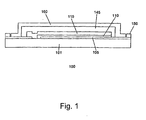
- Fig. 1 shows a conventional pixelated OLED device 100.
- Pixelated OLED devices can be used as displays in various consumer electronic products, including cellular phones, cellular smart phones, personal organizers, pagers, advertising panels, touch screen displays, teleconferencing and multimedia products, virtual reality products, and display kiosks.
- the OLED device comprises a functional stack of one or more organic functional layers 110 between a transparent conductive layer 105 and a conductive layer 115.
- the functional stack is formed on a transparent substrate 101.
- the conductive layers are patterned to form rows of cathodes in a first direction and columns of anodes in a second direction.
- OLED pixels are located where the cathodes and anodes overlap.
- Bond pads 150 are coupled to the cathodes and anodes to control the OLED pixels.
- a cap 160 which forms a cavity 145 between it and the pixels, encapsulates the device to protect the OLED pixels from the environment such as moisture and/or air.
- charge carriers are injected through the cathodes and anodes for recombination in the functional layers.
- the recombination of the charge carriers causes the functional layer of the pixels to emit visible radiation.
- the spacing between pixels should be small, for example, about less than 50 um.
- the spacing between the pixels is defined by the patterning processes that form the cathodes and anodes.
- Various conventional patterning techniques have been used to form the cathodes, such as shadow masking, photolithography (with wet or dry etching), laser ablation, or lift-off techniques (wet or dry resists).
- conventional patterning techniques are not fully compatible or feasible for fabricating OLEDs.
- photolithographic techniques employ chemicals which damage the organic functional layers or cathode materials.
- shadow masking or lift-off techniques wet resists as well as dry resist foils
- high resolutions e.g., less than 50 um are difficult to achieve, particularly in a manufacturing or production environment.
- the invention relates generally to the fabrication of devices such as OLED devices. More particularly, the invention relates to the patterning of a conductive layer.
- pillars with an undercut e.g., cross-section which is wider on top
- the pillars comprise a tapered profile.
- the pillars are formed by photolithography.
- the pillars are formed from a photosensitive material.
- the pillars are inert to the solvents used to deposit the functional organic layers.
- the tapered profile of the pillars patterns a conductive layer into distinct first and second portions during deposition. The first portions are located between the pillars and the second portions are located on the top of the pillars. In one embodiment, the first portions serve as cathodes of an OLED device.
- Fig. 2 shows an OLED device 200 in accordance with one embodiment of the invention.
- the OLED device comprises a substrate 201 on which pixels are formed.
- the substrate comprises a transparent substrate, such as glass. Other types of transparent materials that can serve as a substrate to support the OLED pixels are also useful.
- the OLED pixels comprise one or more organic layers 210 sandwiched between first and second electrodes 205 and 215.
- the first electrodes 205 are anodes and the second electrodes 215 are cathodes. Forming first electrodes that are cathodes and second electrodes that are anodes is also useful.
- the cathodes and anodes are formed as strips in respective first and second directions. Typically, the first and second directions are orthogonal to each other. Bond pads 250 are electrically coupled to the cathodes and anodes.
- a cap 260 is provided to encapsulate the OLED pixels. The cap creates a cavity 245 to protect the pixels from being damaged by physical contact with the cap.
- Pillars 270 are provided on the substrate surface.
- the pillars are arranged in a second direction.
- the height of the pillars extend above the functional stack (e.g., 1-10 um), separating the cathodes and the organic functional layers into strips.
- the pillars can also extend the height of the cavity to serve as support structures for the cap 260. This is particularly useful for flexible OLED devices since the cap is prevented from contacting and damaging the pixels.
- the pillars include an undercut, which results in structures which are wider at the top than at the bottom.
- the undercut serves to pattern a conductive layer 215 during deposition to form distinct or separate portions 215a above the functional layers and portions 215b on the top of the pillars.
- the portions 215a serve as cathodes.
- the undercut is provided by forming pillars with a tapered profile.
- the first and second sidewalls are tapered, producing pillars with a v-shaped cross-section.
- the pillars are formed from a single device layer. Forming the pillars from a single layer advantageously reduces manufacturing cost. Since the chemicals, such as solvents for depositing the functional organic layer or layers can be corrosive, the pillars are formed from a material that maintains its integrity during processing. In one embodiment, the pillars are formed using a photosensitive material such as resist. The resist is treated to render it inert to solvents. Other types of photosensitive materials, such as photosensitive polyimide or photosensitive polybenzosazole, are also useful. In addition, electron cure resist system, such as those manufactured by Allied Signal, can also be used to form pillars having the desired cross-sectional shape.
- Figs. 3-7 show a process for fabricating an OLED device in accordance with one embodiment of the invention.
- a substrate 301 is provided.
- the substrate comprises a transparent substrate, for example, soda lime or borosilicate glass. Other types of transparent materials can also be used to serve as the substrate.
- the substrate typically is about 0.4 - 1.1 mm thick.
- the substrate comprises a thin flexible substrate.
- Thin flexible substrates are formed from, for example, plastic films such as transparent poly(ethylene terephthalate) (PET), poly(butylene terephthalate) (PBT), poly(enthylene naphthalate) (PEN), polycarbonate (PC), polyimides (PI), polysulfones (PSO), and poly( p -phenylene ether sulfone) (PES).
- PET poly(ethylene terephthalate)
- PBT poly(butylene terephthalate)
- PEN poly(enthylene naphthalate)
- PC polycarbonate
- PI polyimides
- PSO polysulfones
- PES poly( p -phenylene ether sulfone)
- Other materials such as polyethylene (PE), polypropylene (PP), poly(vinyl chloride) (PVC), polystyrene (PS) and poly(methyl methyleacrylate) (PMMA
- the substrate includes first electrodes 305 formed on the surface thereof.
- the first electrodes serve as, for example, anodes.
- the anodes are formed from a conductive material.
- the conductive material comprises a transparent conductive material such as indium-tin-oxide (ITO).
- ITO indium-tin-oxide
- Other transparent conductive materials for example, indium-zinc-oxide, zinc-oxide, tin-oxide, are also useful.
- the anodes are arranged in strips in a first direction, each being separated by a space. Preferably, the space separating the anodes is less than 50 um wide. Connections to bond pads can also be provided.
- Various techniques, such as photolithography, can be used to form the anodes.
- a device layer 469 is deposited on the substrate.
- the device layer is used to create the pillars which facilitate patterning of a conductive layer to form the second electrodes (e.g., cathodes).
- the thickness of the device layer is equal to the height of the pillars.
- the thickness of the device layer for example, is about 0.5-50 um, preferably about 1-10 um.
- the device layer comprises a negative acting photoresist such as AZ 5214E manufactured by Clariant. Other photosensitive materials can also be used.
- the resist is deposited on the substrate by, for example, spin-coating. In one embodiment, the resist is deposited by spinning the substrate at 1000 rpm for about 20 seconds using a Karl Suess RC 8 spin-coater. After depositing the resist, the substrate is baked at, for example, 90°C for about 2 minutes to remove the resist solvent.
- the device layer is selectively exposed to light from an exposure source through a mask 520.
- the exposure process is designed to form pillars with the desired undercut or tapered profile.
- the exposure process comprises, for example, successively exposing the photosensitive layer with electrons or charged particles having different energies which have different penetration depths to form the tapered profile during development.
- the exposure comprises selectively exposing the upper regions of the device layer with a lesser amount of energy than the lower regions.
- the exposure comprises selectively exposing the upper regions of the device layer with a greater amount of energy than the lower regions.
- a negative resist layer is selectively exposed with an exposure source.
- the exposure results in the upper portions of regions 566 absorbing a greater amount of light then the lower portions (i.e., underexposing the lower portions of regions 566). Regions 566 correspond to locations where pillars are to be formed.
- the resist is exposed with I line radiation using a Karl Suess MJB 3 exposure source. The exposure dose is about 50 mJ/cm 2 .
- the resist is then prepared for development to remove the unexposed portions.
- the preparation, for a negative acting resist includes a post-exposure bake to cross-link the resist in the exposed regions.
- the post-exposure bake is performed at, for example, about 120°C for about 60-90 seconds. Cross-linking renders the resist insoluble to the resist development chemistry.
- the resist is subjected to a flood exposure from the exposure source (e.g. exposure without mask).
- the flood exposure renders the previously un-exposed portions of the resist soluble.
- the dose of the flood exposure is, for example, about 1000 mJ/cm 2 .
- the device layer is developed with a resist development chemistry to remove the unexposed regions, leaving pillars 670.
- the resist chemistry comprises an alkaline developer such as A2 726 manufactured by Clariant.
- the resist is developed in the development chemistry at room temperature for about 60 seconds. Because the lower parts of the exposed regions were underexposed, they are more soluble to the resist chemistry. This creates pillars with an undercut, resulting in a cross-section that is narrower at the bottom than the top.
- the resist is then rinsed with de-ionized water to remove the developer.
- the resist is cured to improve the mechanical stability of the pillars and to render pillars inert to the organic solvents used to form the functional organic layers.
- the resist is cured by heating the substrate at a temperature of about 160°C for about 6 hours.
- the substrate is cured in accordance with the following parameters:
- a functional organic layer is deposited on the substrate.
- the functional organic layer comprises a conjugated polymer.
- the polymer is dissolved in a solvent and deposited by spin-coating techniques.
- the organic functional layer comprises a 1 % solution of electroluminescent polymer dissolved in xylene deposited by spinning the substrate at 4000 rpm for about 30 seconds.
- Other wet deposition techniques are also useful. Such techniques, for example, include printing techniques (e.g., screen printing, off-set printing, ink-jet printing) in which the organic functional layer is dissolved in a solvent (e.g., NMP, or hexene).
- Depositing the organic functional layer by a wet process is advantageous as it is substantially self planarizing, resulting in the layer filling the area between the pillars with a substantially planar surface.
- the pillars due to curing, are not adversely affected by the solvents.
- Additional functional layers can be deposited to form a functional organic stack.
- the thickness of the organic layer or stack is typically about 2 - 200 nm.
- the substrate is heated to a temperature of about 85°C for about 1 minute to evaporate the solvent.
- Portions of the organic layer can be selectively removed, for example, to expose underlying layers in regions 470 for bond pad connections. Selective removal of the organic layers can be achieved by a polishing process. Other techniques, such as etching, scratching, or laser ablation, can also be used to selectively remove portions of the organic layers.
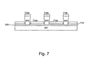
- a conductive layer 715 is deposited on the substrate.
- the conductive layer comprises, for example, Ca, Mg, Ba, Ag, Al or a mixture or alloy thereof.
- Other conductive materials particularly those comprising a low work function, can also be used to form the second conductive layer.
- the second conductive layer comprises Ca.
- the Ca is deposited by thermal evaporation at a rate of 1 nm/s and a pressure of about 10 -5 mbar.
- Other deposition techniques such as sputtering (PVD), chemical vapor deposition (CVD), plasma enhanced chemical vapor deposition (PECVD) or metal organic chemical vapor deposition (MOCVD), are also useful.
- the deposition of the conductive layer is interrupted due to the height and profile of the pillars, resulting in parts 715a of the conductive layer being deposited in regions between the pillars and parts 715b of the conductive layer being formed on the top surface of the pillars.
- the parts of the conductive layer between the pillars serve as cathodes. The intersections of the cathodes and anodes form organic LED pixels.
- a cavity cap is mounted on the substrate to encapsulate the device and bond pads are formed to provide electrical access to the OLED pixels.
Applications Claiming Priority (1)
| Application Number | Priority Date | Filing Date | Title |
|---|---|---|---|
| PCT/SG2000/000134 WO2002021883A1 (en) | 2000-09-06 | 2000-09-06 | Patterning of electrodes in oled devices |
Publications (2)
| Publication Number | Publication Date |
|---|---|
| EP1317874A1 EP1317874A1 (en) | 2003-06-11 |
| EP1317874B1 true EP1317874B1 (en) | 2004-05-06 |
Family
ID=20428858
Family Applications (1)
| Application Number | Title | Priority Date | Filing Date |
|---|---|---|---|
| EP00963240A Expired - Lifetime EP1317874B1 (en) | 2000-09-06 | 2000-09-06 | Patterning of electrodes in oled devices |
Country Status (8)
| Country | Link |
|---|---|
| US (1) | US7057337B1 (zh) |
| EP (1) | EP1317874B1 (zh) |
| JP (1) | JP2004508691A (zh) |
| CN (1) | CN100431196C (zh) |
| AU (1) | AU2000274683A1 (zh) |
| DE (1) | DE60010531T2 (zh) |
| TW (1) | TW512547B (zh) |
| WO (1) | WO2002021883A1 (zh) |
Families Citing this family (32)
| Publication number | Priority date | Publication date | Assignee | Title |
|---|---|---|---|---|
| US6699728B2 (en) | 2000-09-06 | 2004-03-02 | Osram Opto Semiconductors Gmbh | Patterning of electrodes in oled devices |
| TW586141B (en) * | 2001-01-19 | 2004-05-01 | Semiconductor Energy Lab | Semiconductor device and method of manufacturing the same |
| US7148624B2 (en) | 2002-05-07 | 2006-12-12 | Osram Opto Semiconductors (Malaysia) Sdn. Bhd | Uniform deposition of organic layer |
| US7423375B2 (en) | 2002-05-07 | 2008-09-09 | Osram Gmbh | Encapsulation for electroluminescent devices |
| KR100875097B1 (ko) | 2002-09-18 | 2008-12-19 | 삼성모바일디스플레이주식회사 | 광학 공진 효과를 이용한 유기 전계발광 소자 |
| US7026660B2 (en) | 2003-04-25 | 2006-04-11 | Osram Opto Semiconductors (Malaysia) Sdn. Bhd | Interconnection for organic devices |
| US8025831B2 (en) | 2004-05-24 | 2011-09-27 | Agency For Science, Technology And Research | Imprinting of supported and free-standing 3-D micro- or nano-structures |
| US6992326B1 (en) | 2004-08-03 | 2006-01-31 | Dupont Displays, Inc. | Electronic device and process for forming same |
| US7166860B2 (en) | 2004-12-30 | 2007-01-23 | E. I. Du Pont De Nemours And Company | Electronic device and process for forming same |
| DE102005039528A1 (de) * | 2005-08-18 | 2007-02-22 | Merck Patent Gmbh | Lösungen organischer Halbleiter |
| JP2008273211A (ja) * | 2008-05-19 | 2008-11-13 | Nitto Denko Corp | 透明ガスバリア性部材及びこれを用いた有機エレクトロルミネッセンス素子 |
| EP2613376A4 (en) * | 2010-09-02 | 2014-08-27 | Showa Denko Kk | LIGHT EMITTING ELEMENT, METHOD FOR MANUFACTURING LIGHT EMITTING ELEMENT, DISPLAY DEVICE, AND LIGHTING DEVICE |
| US9389315B2 (en) | 2012-12-19 | 2016-07-12 | Basf Se | Detector comprising a transversal optical sensor for detecting a transversal position of a light beam from an object and a longitudinal optical sensor sensing a beam cross-section of the light beam in a sensor region |
| AU2014280335B2 (en) | 2013-06-13 | 2018-03-22 | Basf Se | Detector for optically detecting an orientation of at least one object |
| CN109521397B (zh) | 2013-06-13 | 2023-03-28 | 巴斯夫欧洲公司 | 用于光学地检测至少一个对象的检测器 |
| AU2014280334B2 (en) * | 2013-06-13 | 2018-02-01 | Basf Se | Optical detector and method for manufacturing the same |
| CN105637320B (zh) | 2013-08-19 | 2018-12-14 | 巴斯夫欧洲公司 | 光学检测器 |
| US10185171B2 (en) | 2014-06-04 | 2019-01-22 | Sharp Kabushiki Kaisha | Light control member, method of manufacturing light control member, apparatus for manufacturing light control member, and display device |
| CN106662636B (zh) | 2014-07-08 | 2020-12-25 | 巴斯夫欧洲公司 | 用于确定至少一个对象的位置的检测器 |
| WO2016051323A1 (en) | 2014-09-29 | 2016-04-07 | Basf Se | Detector for optically determining a position of at least one object |
| EP3230841B1 (en) | 2014-12-09 | 2019-07-03 | Basf Se | Optical detector |
| JP6841769B2 (ja) | 2015-01-30 | 2021-03-10 | トリナミクス ゲゼルシャフト ミット ベシュレンクテル ハフツング | 少なくとも1個の物体を光学的に検出する検出器 |
| US10955936B2 (en) | 2015-07-17 | 2021-03-23 | Trinamix Gmbh | Detector for optically detecting at least one object |
| KR102539263B1 (ko) | 2015-09-14 | 2023-06-05 | 트리나미엑스 게엠베하 | 적어도 하나의 물체의 적어도 하나의 이미지를 기록하는 카메라 |
| JP2019523562A (ja) | 2016-07-29 | 2019-08-22 | トリナミクス ゲゼルシャフト ミット ベシュレンクテル ハフツング | 光学的検出のための光センサおよび検出器 |
| JP7241684B2 (ja) | 2016-10-25 | 2023-03-17 | トリナミクス ゲゼルシャフト ミット ベシュレンクテル ハフツング | 少なくとも1個の対象物の光学的な検出のための検出器 |
| KR102575104B1 (ko) | 2016-10-25 | 2023-09-07 | 트리나미엑스 게엠베하 | 집적 필터를 가진 적외선 광학 검출기 |
| US11860292B2 (en) | 2016-11-17 | 2024-01-02 | Trinamix Gmbh | Detector and methods for authenticating at least one object |
| US11415661B2 (en) | 2016-11-17 | 2022-08-16 | Trinamix Gmbh | Detector for optically detecting at least one object |
| US11060922B2 (en) | 2017-04-20 | 2021-07-13 | Trinamix Gmbh | Optical detector |
| JP7237024B2 (ja) | 2017-06-26 | 2023-03-10 | トリナミクス ゲゼルシャフト ミット ベシュレンクテル ハフツング | 少なくとも1つの物体の位置を決定するための検出器 |
| JP2022185322A (ja) * | 2021-06-02 | 2022-12-14 | 株式会社ジャパンディスプレイ | 電子機器及びその製造方法 |
Family Cites Families (15)
| Publication number | Priority date | Publication date | Assignee | Title |
|---|---|---|---|---|
| JP2602323B2 (ja) * | 1989-03-31 | 1997-04-23 | 東洋インキ製造株式会社 | カラーフィルターの製造方法 |
| GB8909011D0 (en) * | 1989-04-20 | 1989-06-07 | Friend Richard H | Electroluminescent devices |
| JP3813217B2 (ja) * | 1995-03-13 | 2006-08-23 | パイオニア株式会社 | 有機エレクトロルミネッセンスディスプレイパネルの製造方法 |
| US5701055A (en) * | 1994-03-13 | 1997-12-23 | Pioneer Electronic Corporation | Organic electoluminescent display panel and method for manufacturing the same |
| US5641611A (en) | 1995-08-21 | 1997-06-24 | Motorola | Method of fabricating organic LED matrices |
| JP3886219B2 (ja) * | 1997-07-29 | 2007-02-28 | 株式会社アルバック | 有機el素子 |
| JP3633229B2 (ja) * | 1997-09-01 | 2005-03-30 | セイコーエプソン株式会社 | 発光素子の製造方法および多色表示装置の製造方法 |
| US6278237B1 (en) | 1997-09-22 | 2001-08-21 | Emagin Corporation | Laterally structured high resolution multicolor organic electroluminescence display device |
| TW432896B (en) * | 1997-10-15 | 2001-05-01 | Siemens Ag | Preparation of organic electroluminescencizing elements |
| JP3663876B2 (ja) * | 1998-01-08 | 2005-06-22 | 松下電器産業株式会社 | 有機エレクトロルミネセンス素子及びその製造方法 |
| JPH11283752A (ja) | 1998-03-27 | 1999-10-15 | Futaba Corp | 有機エレクトロルミネッセンス素子 |
| US6111356A (en) * | 1998-04-13 | 2000-08-29 | Agilent Technologies, Inc. | Method for fabricating pixelated polymer organic light emitting devices |
| GB9808806D0 (en) * | 1998-04-24 | 1998-06-24 | Cambridge Display Tech Ltd | Selective deposition of polymer films |
| US6306559B1 (en) * | 1999-01-26 | 2001-10-23 | Mitsubishi Chemical Corporation | Organic electroluminescent device comprising a patterned photosensitive composition and a method for producing same |
| US6699728B2 (en) | 2000-09-06 | 2004-03-02 | Osram Opto Semiconductors Gmbh | Patterning of electrodes in oled devices |
-
2000
- 2000-09-06 US US10/363,200 patent/US7057337B1/en not_active Expired - Lifetime
- 2000-09-06 CN CNB008198764A patent/CN100431196C/zh not_active Expired - Lifetime
- 2000-09-06 DE DE60010531T patent/DE60010531T2/de not_active Expired - Lifetime
- 2000-09-06 AU AU2000274683A patent/AU2000274683A1/en not_active Abandoned
- 2000-09-06 JP JP2002526157A patent/JP2004508691A/ja active Pending
- 2000-09-06 EP EP00963240A patent/EP1317874B1/en not_active Expired - Lifetime
- 2000-09-06 WO PCT/SG2000/000134 patent/WO2002021883A1/en active IP Right Grant
-
2001
- 2001-09-07 TW TW090122225A patent/TW512547B/zh not_active IP Right Cessation
Also Published As
| Publication number | Publication date |
|---|---|
| CN1454447A (zh) | 2003-11-05 |
| DE60010531T2 (de) | 2005-05-12 |
| WO2002021883A1 (en) | 2002-03-14 |
| JP2004508691A (ja) | 2004-03-18 |
| DE60010531D1 (de) | 2004-06-09 |
| EP1317874A1 (en) | 2003-06-11 |
| AU2000274683A1 (en) | 2002-03-22 |
| US7057337B1 (en) | 2006-06-06 |
| TW512547B (en) | 2002-12-01 |
| CN100431196C (zh) | 2008-11-05 |
Similar Documents
| Publication | Publication Date | Title |
|---|---|---|
| EP1317874B1 (en) | Patterning of electrodes in oled devices | |
| US6784009B2 (en) | Electrode patterning in OLED devices | |
| US20070190682A1 (en) | Patterning of electrodes in oled devices | |
| US6911667B2 (en) | Encapsulation for organic electronic devices | |
| JP4520708B2 (ja) | 基板上に作製される複数のデバイスを封入する方法および電子デバイス | |
| JP3948082B2 (ja) | 有機エレクトロルミネッセンス素子の製造方法 | |
| US7423375B2 (en) | Encapsulation for electroluminescent devices | |
| US7737631B2 (en) | Flat panel display with repellant and border areas and method of manufacturing the same | |
| WO2001044865A1 (en) | Improved encapsulation for organic led device | |
| EP1502311B1 (en) | Organic device | |
| KR100762121B1 (ko) | 유기 전계 발광 소자의 제조 방법 | |
| CN111668272A (zh) | 显示基板及其制备方法 | |
| KR100413856B1 (ko) | 유기 전계 발광 소자 및 그의 제조 방법 | |
| WO2007142603A1 (en) | An integrated shadow mask and method of fabrication thereof | |
| KR100415433B1 (ko) | 유기 전계 발광 소자 및 그의 제조 방법 | |
| KR20030030792A (ko) | 유기 전계 발광 소자 및 그의 제조 방법 |
Legal Events
| Date | Code | Title | Description |
|---|---|---|---|
| PUAI | Public reference made under article 153(3) epc to a published international application that has entered the european phase |
Free format text: ORIGINAL CODE: 0009012 |
|
| 17P | Request for examination filed |
Effective date: 20030203 |
|
| AK | Designated contracting states |
Designated state(s): AT BE CH CY DE DK ES FI FR GB GR IE IT LI LU MC NL PT SE |
|
| AX | Request for extension of the european patent |
Extension state: AL LT LV MK RO SI |
|
| RAP1 | Party data changed (applicant data changed or rights of an application transferred) |
Owner name: OSRAM OPTO SEMICONDUCTORS GMBH |
|
| GRAP | Despatch of communication of intention to grant a patent |
Free format text: ORIGINAL CODE: EPIDOSNIGR1 |
|
| GRAS | Grant fee paid |
Free format text: ORIGINAL CODE: EPIDOSNIGR3 |
|
| GRAA | (expected) grant |
Free format text: ORIGINAL CODE: 0009210 |
|
| AK | Designated contracting states |
Kind code of ref document: B1 Designated state(s): DE FR GB |
|
| RBV | Designated contracting states (corrected) |
Designated state(s): DE FR GB |
|
| REG | Reference to a national code |
Ref country code: GB Ref legal event code: FG4D |
|
| REF | Corresponds to: |
Ref document number: 60010531 Country of ref document: DE Date of ref document: 20040609 Kind code of ref document: P |
|
| REG | Reference to a national code |
Ref country code: IE Ref legal event code: FG4D |
|
| ET | Fr: translation filed | ||
| PLBE | No opposition filed within time limit |
Free format text: ORIGINAL CODE: 0009261 |
|
| STAA | Information on the status of an ep patent application or granted ep patent |
Free format text: STATUS: NO OPPOSITION FILED WITHIN TIME LIMIT |
|
| 26N | No opposition filed |
Effective date: 20050208 |
|
| REG | Reference to a national code |
Ref country code: IE Ref legal event code: MM4A |
|
| REG | Reference to a national code |
Ref country code: FR Ref legal event code: PLFP Year of fee payment: 17 |
|
| REG | Reference to a national code |
Ref country code: FR Ref legal event code: PLFP Year of fee payment: 18 |
|
| PGFP | Annual fee paid to national office [announced via postgrant information from national office to epo] |
Ref country code: GB Payment date: 20170921 Year of fee payment: 18 Ref country code: FR Payment date: 20170928 Year of fee payment: 18 |
|
| GBPC | Gb: european patent ceased through non-payment of renewal fee |
Effective date: 20180906 |
|
| PG25 | Lapsed in a contracting state [announced via postgrant information from national office to epo] |
Ref country code: FR Free format text: LAPSE BECAUSE OF NON-PAYMENT OF DUE FEES Effective date: 20180930 |
|
| PG25 | Lapsed in a contracting state [announced via postgrant information from national office to epo] |
Ref country code: GB Free format text: LAPSE BECAUSE OF NON-PAYMENT OF DUE FEES Effective date: 20180906 |
|
| PGFP | Annual fee paid to national office [announced via postgrant information from national office to epo] |
Ref country code: DE Payment date: 20190918 Year of fee payment: 20 |
|
| REG | Reference to a national code |
Ref country code: DE Ref legal event code: R081 Ref document number: 60010531 Country of ref document: DE Owner name: OSRAM OLED GMBH, DE Free format text: FORMER OWNER: OSRAM OPTO SEMICONDUCTORS GESELLSCHAFT MIT BESCHRAENKTER HAFTUNG, 93055 REGENSBURG, DE Ref country code: DE Ref legal event code: R082 Ref document number: 60010531 Country of ref document: DE Representative=s name: EPPING HERMANN FISCHER PATENTANWALTSGESELLSCHA, DE Ref country code: DE Ref legal event code: R081 Ref document number: 60010531 Country of ref document: DE Owner name: PICTIVA DISPLAYS INTERNATIONAL LIMITED, IE Free format text: FORMER OWNER: OSRAM OPTO SEMICONDUCTORS GESELLSCHAFT MIT BESCHRAENKTER HAFTUNG, 93055 REGENSBURG, DE |
|
| REG | Reference to a national code |
Ref country code: DE Ref legal event code: R071 Ref document number: 60010531 Country of ref document: DE |
|
| REG | Reference to a national code |
Ref country code: DE Ref legal event code: R081 Ref document number: 60010531 Country of ref document: DE Owner name: PICTIVA DISPLAYS INTERNATIONAL LIMITED, IE Free format text: FORMER OWNER: OSRAM OLED GMBH, 93049 REGENSBURG, DE Ref country code: DE Ref legal event code: R082 Ref document number: 60010531 Country of ref document: DE Representative=s name: EPPING HERMANN FISCHER PATENTANWALTSGESELLSCHA, DE |