EP1315287B1 - A low noise biasing technique - Google Patents
A low noise biasing technique Download PDFInfo
- Publication number
- EP1315287B1 EP1315287B1 EP02019119A EP02019119A EP1315287B1 EP 1315287 B1 EP1315287 B1 EP 1315287B1 EP 02019119 A EP02019119 A EP 02019119A EP 02019119 A EP02019119 A EP 02019119A EP 1315287 B1 EP1315287 B1 EP 1315287B1
- Authority
- EP
- European Patent Office
- Prior art keywords
- interposed
- node
- ground
- transistor
- inductor
- Prior art date
- Legal status (The legal status is an assumption and is not a legal conclusion. Google has not performed a legal analysis and makes no representation as to the accuracy of the status listed.)
- Expired - Lifetime
Links
Images
Classifications
-
- G—PHYSICS
- G05—CONTROLLING; REGULATING
- G05F—SYSTEMS FOR REGULATING ELECTRIC OR MAGNETIC VARIABLES
- G05F3/00—Non-retroactive systems for regulating electric variables by using an uncontrolled element, or an uncontrolled combination of elements, such element or such combination having self-regulating properties
- G05F3/02—Regulating voltage or current
- G05F3/08—Regulating voltage or current wherein the variable is DC
- G05F3/10—Regulating voltage or current wherein the variable is DC using uncontrolled devices with non-linear characteristics
- G05F3/16—Regulating voltage or current wherein the variable is DC using uncontrolled devices with non-linear characteristics being semiconductor devices
- G05F3/20—Regulating voltage or current wherein the variable is DC using uncontrolled devices with non-linear characteristics being semiconductor devices using diode- transistor combinations
- G05F3/26—Current mirrors
- G05F3/262—Current mirrors using field-effect transistors only
Definitions
- One of the common ways to provide gate bias to an enhancement mode Field Effect Transistor is to use a current mirror.
- the current mirror is itself a source of unwanted noise.
- This resistor (Ri) can cause a reduction in the power handling capacity of the amplifier transistor.
- the amplifier transistor attempts to draw more current. This action requires more current through the gate of the field effect transistor (FET), dropping voltage across Ri. As the voltage increases across Ri, the voltage available to the input of the amplifier transistor is reduced. The voltage at the input sets the current through the amplifier, and so this reduction lowers the power handling capacity of the amplifier. This is a significant source of distortion.
- the distortion is another noise source.
- a large resistor minimizes the noise injected into the amplifier from the bias network but a small resistor minimizes the noise due to distortion. The compromise can be difficult to find.
- examples for biasing a field effect transistor are disclosed e.g. in EP 606094 and US 6288596 .
- a first transistor has a drain and gate tied together at a first node. Its source is connected to ground.
- a current-setting resistor connects the first node and an RF output.
- a first capacitor connects node A and ground.
- a first inductor connects an RF input and node A.
- the second transistor has a drain connected to the RF output and a source connected to ground.
- a second inductor connects the gate of the second transistor and the RF input.
- a third inductor is interposed between power and the RF output.
- a second capacitor is interposed between power and ground.
- a first transistor has a drain and gate tied together at node B. The source of the first transistor is connected to ground. A first capacitor connects node B and ground. A second transistor has a drain connected to a RF output and a source connected to ground. A current setting resistor is interposed between power and node B. A first inductor is interposed between node B and a RF input. A second inductor connects the gate of the second transistor and the RF input. A third inductor is interposed between power and the RF output. A second capacitor is interposed between power and ground.
- the first and second transistors are formed on a unitary substrate.
- the current setting resistor may be optionally integrated onto the unitary substrate.
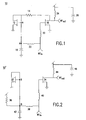
- Figure 1 illustrates a first circuit topology 10 according to the present invention.
- a first transistor 12 has a drain and gate tied together at a first node A. Its source is connected to ground.
- a current-setting resistor 14 connects the first node A and an RF output.
- a first capacitor 18 connects node A and ground.
- a first inductor 22 connects an RF input and node A.
- the second transistor 16 has a drain connected to the RF output and a source connected to ground.
- a second inductor 20 connects the gate of the second transistor and the RF input.
- a third inductor 24 is interposed between power and the RF output.
- a second capacitor 26 is interposed between power and ground.
- the first and second transistors 12, 16 are formed on a unitary substrate (not shown).
- the current-setting resistor 14 may be optionally integrated onto the unitary substrate.
- Figure 2 illustrates an alternate embodiment 10' of the present invention.
- a first transistor 32 has a drain and gate tied together at node B. The source of the first transistor 32 is connected to ground.
- a first capacitor 42 connects node B and ground.
- a second transistor 34 has a drain connected to a RF output and a source connected to ground.
- a current setting resistor 36 is interposed between power and node B.
- a first inductor 38 is interposed between node B and a RF input.
- a second inductor 40 connects the gate of the second transistor 34 and the RF input.
- a third inductor 44 is interposed between power and the RF output.
- a second capacitor 46 is interposed between power and ground.
- the first and second transistors 32, 36 are formed on a unitary substrate.
- the current setting resistor 36 may be integrated onto the unitary substrate.
- the current mirror voltage is sampled by an off-chip inductor 24, 44.
- This inductor can be part of the typical matching network required by the amplifier. The only extra component required is a package pin to get this node outside. If an external current setting resistor Rcs is desirable, then this extra pin is already required and can be used for both functions.
- the first and second transistors are preferably enhancement mode field effect transistors.
Landscapes
- Engineering & Computer Science (AREA)
- Microelectronics & Electronic Packaging (AREA)
- Physics & Mathematics (AREA)
- Nonlinear Science (AREA)
- Electromagnetism (AREA)
- General Physics & Mathematics (AREA)
- Radar, Positioning & Navigation (AREA)
- Automation & Control Theory (AREA)
- Amplifiers (AREA)
Applications Claiming Priority (2)
| Application Number | Priority Date | Filing Date | Title |
|---|---|---|---|
| US10359 | 1987-02-03 | ||
| US10/010,359 US6452370B1 (en) | 2001-11-13 | 2001-11-13 | Low noise biasing technique |
Publications (3)
| Publication Number | Publication Date |
|---|---|
| EP1315287A2 EP1315287A2 (en) | 2003-05-28 |
| EP1315287A3 EP1315287A3 (en) | 2004-08-18 |
| EP1315287B1 true EP1315287B1 (en) | 2008-05-21 |
Family
ID=21745380
Family Applications (1)
| Application Number | Title | Priority Date | Filing Date |
|---|---|---|---|
| EP02019119A Expired - Lifetime EP1315287B1 (en) | 2001-11-13 | 2002-08-29 | A low noise biasing technique |
Country Status (4)
| Country | Link |
|---|---|
| US (1) | US6452370B1 (OSRAM) |
| EP (1) | EP1315287B1 (OSRAM) |
| JP (1) | JP2003152473A (OSRAM) |
| DE (1) | DE60226690D1 (OSRAM) |
Families Citing this family (2)
| Publication number | Priority date | Publication date | Assignee | Title |
|---|---|---|---|---|
| US7847424B2 (en) * | 2007-06-12 | 2010-12-07 | General Electric Company | Circuit and method for reducing a voltage being developed across a field winding of a synchronous machine |
| US7489191B2 (en) | 2007-06-08 | 2009-02-10 | General Electric Company | Circuit and method for reducing bias noise in amplifier circuits |
Family Cites Families (3)
| Publication number | Priority date | Publication date | Assignee | Title |
|---|---|---|---|---|
| US4961006A (en) * | 1989-06-22 | 1990-10-02 | Motorola, Inc. | Inductively loaded switching transistor circuit |
| EP0606094B1 (en) * | 1993-01-08 | 1999-10-06 | Sony Corporation | Monolithic microwave integrated circuit |
| SE516012C2 (sv) * | 1999-01-25 | 2001-11-05 | Ericsson Telefon Ab L M | Styreförspänningsanordning |
-
2001
- 2001-11-13 US US10/010,359 patent/US6452370B1/en not_active Expired - Lifetime
-
2002
- 2002-08-29 EP EP02019119A patent/EP1315287B1/en not_active Expired - Lifetime
- 2002-08-29 DE DE60226690T patent/DE60226690D1/de not_active Expired - Fee Related
- 2002-10-21 JP JP2002306114A patent/JP2003152473A/ja not_active Withdrawn
Also Published As
| Publication number | Publication date |
|---|---|
| US6452370B1 (en) | 2002-09-17 |
| EP1315287A2 (en) | 2003-05-28 |
| EP1315287A3 (en) | 2004-08-18 |
| JP2003152473A (ja) | 2003-05-23 |
| DE60226690D1 (de) | 2008-07-03 |
Similar Documents
| Publication | Publication Date | Title |
|---|---|---|
| KR100389465B1 (ko) | 스위치회로및복합스위치회로 | |
| TWI327416B (en) | Cascode low noise amplifier with a source coupled active inductor | |
| KR100305917B1 (ko) | 반도체전력증폭집적회로 | |
| US7026858B2 (en) | Switch semiconductor integrated circuit | |
| US6285257B1 (en) | Feedback type variable gain amplifier | |
| JP2004274108A (ja) | 利得可変型増幅器 | |
| US7202749B2 (en) | AC coupling technique for improved noise performance and simple biasing | |
| EP0700152A1 (en) | Impedance matching circuit | |
| US20060071704A1 (en) | Amplifying circuit | |
| WO2004049555B1 (en) | Radio frequency power amplifier active self-bias compensation circuit | |
| JP4430246B2 (ja) | 電界効果トランジスタのためのバイアス構成 | |
| US6288596B1 (en) | Gate biasing arrangement to temperature compensate a quiescent current of a power transistor | |
| US6452370B1 (en) | Low noise biasing technique | |
| US6104247A (en) | Power amplifier for mobile communication system | |
| JP3105489B2 (ja) | 増幅器 | |
| US20010009390A1 (en) | OW current amplifier circuit with protection against static electricity | |
| KR200308685Y1 (ko) | 저잡음증폭기 | |
| JP3922950B2 (ja) | 周波数変換回路 | |
| JPH11150464A (ja) | 半導体スイッチ回路、この回路の制御方法及びアッテネータ回路 | |
| JP2001068950A (ja) | ゲートバイアス回路 | |
| JP2013034090A (ja) | 増幅器 | |
| JP3864477B2 (ja) | 高周波回路 | |
| JPH06276038A (ja) | 高周波低雑音増幅器 | |
| JP3176793B2 (ja) | 増幅回路 | |
| JPH0846446A (ja) | ゲートバイアス回路 |
Legal Events
| Date | Code | Title | Description |
|---|---|---|---|
| PUAI | Public reference made under article 153(3) epc to a published international application that has entered the european phase |
Free format text: ORIGINAL CODE: 0009012 |
|
| AK | Designated contracting states |
Designated state(s): AT BE BG CH CY CZ DE DK EE ES FI FR GB GR IE IT LI LU MC NL PT SE SK TR |
|
| AX | Request for extension of the european patent |
Extension state: AL LT LV MK RO SI |
|
| PUAL | Search report despatched |
Free format text: ORIGINAL CODE: 0009013 |
|
| AK | Designated contracting states |
Kind code of ref document: A3 Designated state(s): AT BE BG CH CY CZ DE DK EE ES FI FR GB GR IE IT LI LU MC NL PT SE SK TR |
|
| AX | Request for extension of the european patent |
Extension state: AL LT LV MK RO SI |
|
| 17P | Request for examination filed |
Effective date: 20040921 |
|
| AKX | Designation fees paid |
Designated state(s): DE FI GB |
|
| RBV | Designated contracting states (corrected) |
Designated state(s): DE FI GB |
|
| RAP1 | Party data changed (applicant data changed or rights of an application transferred) |
Owner name: AVAGO TECHNOLOGIES WIRELESS IP (SINGAPORE) PTE. LT |
|
| GRAP | Despatch of communication of intention to grant a patent |
Free format text: ORIGINAL CODE: EPIDOSNIGR1 |
|
| GRAS | Grant fee paid |
Free format text: ORIGINAL CODE: EPIDOSNIGR3 |
|
| GRAA | (expected) grant |
Free format text: ORIGINAL CODE: 0009210 |
|
| AK | Designated contracting states |
Kind code of ref document: B1 Designated state(s): DE FI GB |
|
| REG | Reference to a national code |
Ref country code: GB Ref legal event code: FG4D |
|
| REF | Corresponds to: |
Ref document number: 60226690 Country of ref document: DE Date of ref document: 20080703 Kind code of ref document: P |
|
| PG25 | Lapsed in a contracting state [announced via postgrant information from national office to epo] |
Ref country code: FI Free format text: LAPSE BECAUSE OF FAILURE TO SUBMIT A TRANSLATION OF THE DESCRIPTION OR TO PAY THE FEE WITHIN THE PRESCRIBED TIME-LIMIT Effective date: 20080521 |
|
| PLBE | No opposition filed within time limit |
Free format text: ORIGINAL CODE: 0009261 |
|
| STAA | Information on the status of an ep patent application or granted ep patent |
Free format text: STATUS: NO OPPOSITION FILED WITHIN TIME LIMIT |
|
| 26N | No opposition filed |
Effective date: 20090224 |
|
| GBPC | Gb: european patent ceased through non-payment of renewal fee |
Effective date: 20080829 |
|
| PG25 | Lapsed in a contracting state [announced via postgrant information from national office to epo] |
Ref country code: DE Free format text: LAPSE BECAUSE OF NON-PAYMENT OF DUE FEES Effective date: 20090303 |
|
| PG25 | Lapsed in a contracting state [announced via postgrant information from national office to epo] |
Ref country code: GB Free format text: LAPSE BECAUSE OF NON-PAYMENT OF DUE FEES Effective date: 20080829 |