EP1300880A2 - Verfahren zum photolithographischen Festlegen eines freigelegten Substratbereichs - Google Patents
Verfahren zum photolithographischen Festlegen eines freigelegten Substratbereichs Download PDFInfo
- Publication number
- EP1300880A2 EP1300880A2 EP02019495A EP02019495A EP1300880A2 EP 1300880 A2 EP1300880 A2 EP 1300880A2 EP 02019495 A EP02019495 A EP 02019495A EP 02019495 A EP02019495 A EP 02019495A EP 1300880 A2 EP1300880 A2 EP 1300880A2
- Authority
- EP
- European Patent Office
- Prior art keywords
- drain
- gate
- substrate
- masking layer
- layer
- Prior art date
- Legal status (The legal status is an assumption and is not a legal conclusion. Google has not performed a legal analysis and makes no representation as to the accuracy of the status listed.)
- Withdrawn
Links
Images











Classifications
-
- H—ELECTRICITY
- H10—SEMICONDUCTOR DEVICES; ELECTRIC SOLID-STATE DEVICES NOT OTHERWISE PROVIDED FOR
- H10D—INORGANIC ELECTRIC SEMICONDUCTOR DEVICES
- H10D30/00—Field-effect transistors [FET]
- H10D30/01—Manufacture or treatment
- H10D30/021—Manufacture or treatment of FETs having insulated gates [IGFET]
- H10D30/0223—Manufacture or treatment of FETs having insulated gates [IGFET] having source and drain regions or source and drain extensions self-aligned to sides of the gate
- H10D30/0225—Manufacture or treatment of FETs having insulated gates [IGFET] having source and drain regions or source and drain extensions self-aligned to sides of the gate using an initial gate mask complementary to the prospective gate location, e.g. using dummy source and drain electrodes
-
- H—ELECTRICITY
- H10—SEMICONDUCTOR DEVICES; ELECTRIC SOLID-STATE DEVICES NOT OTHERWISE PROVIDED FOR
- H10D—INORGANIC ELECTRIC SEMICONDUCTOR DEVICES
- H10D30/00—Field-effect transistors [FET]
- H10D30/01—Manufacture or treatment
- H10D30/021—Manufacture or treatment of FETs having insulated gates [IGFET]
- H10D30/0221—Manufacture or treatment of FETs having insulated gates [IGFET] having asymmetry in the channel direction, e.g. lateral high-voltage MISFETs having drain offset region or extended-drain MOSFETs [EDMOS]
-
- H—ELECTRICITY
- H10—SEMICONDUCTOR DEVICES; ELECTRIC SOLID-STATE DEVICES NOT OTHERWISE PROVIDED FOR
- H10D—INORGANIC ELECTRIC SEMICONDUCTOR DEVICES
- H10D30/00—Field-effect transistors [FET]
- H10D30/60—Insulated-gate field-effect transistors [IGFET]
- H10D30/601—Insulated-gate field-effect transistors [IGFET] having lightly-doped drain or source extensions, e.g. LDD IGFETs or DDD IGFETs
- H10D30/603—Insulated-gate field-effect transistors [IGFET] having lightly-doped drain or source extensions, e.g. LDD IGFETs or DDD IGFETs having asymmetry in the channel direction, e.g. lateral high-voltage MISFETs having drain offset region or extended drain IGFETs [EDMOS]
-
- H—ELECTRICITY
- H10—SEMICONDUCTOR DEVICES; ELECTRIC SOLID-STATE DEVICES NOT OTHERWISE PROVIDED FOR
- H10D—INORGANIC ELECTRIC SEMICONDUCTOR DEVICES
- H10D64/00—Electrodes of devices having potential barriers
- H10D64/01—Manufacture or treatment
- H10D64/013—Manufacture or treatment of electrodes having a conductor capacitively coupled to a semiconductor by an insulator
- H10D64/01302—Manufacture or treatment of electrodes having a conductor capacitively coupled to a semiconductor by an insulator the insulator being formed after the semiconductor body, the semiconductor being silicon
- H10D64/01304—Manufacture or treatment of electrodes having a conductor capacitively coupled to a semiconductor by an insulator the insulator being formed after the semiconductor body, the semiconductor being silicon characterised by the conductor
- H10D64/01326—Aspects related to lithography, isolation or planarisation of the conductor
-
- H—ELECTRICITY
- H10—SEMICONDUCTOR DEVICES; ELECTRIC SOLID-STATE DEVICES NOT OTHERWISE PROVIDED FOR
- H10D—INORGANIC ELECTRIC SEMICONDUCTOR DEVICES
- H10D64/00—Electrodes of devices having potential barriers
- H10D64/01—Manufacture or treatment
- H10D64/017—Manufacture or treatment using dummy gates in processes wherein at least parts of the final gates are self-aligned to the dummy gates, i.e. replacement gate processes
-
- H—ELECTRICITY
- H10—SEMICONDUCTOR DEVICES; ELECTRIC SOLID-STATE DEVICES NOT OTHERWISE PROVIDED FOR
- H10P—GENERIC PROCESSES OR APPARATUS FOR THE MANUFACTURE OR TREATMENT OF DEVICES COVERED BY CLASS H10
- H10P50/00—Etching of wafers, substrates or parts of devices
- H10P50/73—Etching of wafers, substrates or parts of devices using masks for insulating materials
-
- H—ELECTRICITY
- H10—SEMICONDUCTOR DEVICES; ELECTRIC SOLID-STATE DEVICES NOT OTHERWISE PROVIDED FOR
- H10P—GENERIC PROCESSES OR APPARATUS FOR THE MANUFACTURE OR TREATMENT OF DEVICES COVERED BY CLASS H10
- H10P76/00—Manufacture or treatment of masks on semiconductor bodies, e.g. by lithography or photolithography
- H10P76/20—Manufacture or treatment of masks on semiconductor bodies, e.g. by lithography or photolithography of masks comprising organic materials
-
- H—ELECTRICITY
- H10—SEMICONDUCTOR DEVICES; ELECTRIC SOLID-STATE DEVICES NOT OTHERWISE PROVIDED FOR
- H10P—GENERIC PROCESSES OR APPARATUS FOR THE MANUFACTURE OR TREATMENT OF DEVICES COVERED BY CLASS H10
- H10P76/00—Manufacture or treatment of masks on semiconductor bodies, e.g. by lithography or photolithography
- H10P76/40—Manufacture or treatment of masks on semiconductor bodies, e.g. by lithography or photolithography of masks comprising inorganic materials
-
- H—ELECTRICITY
- H10—SEMICONDUCTOR DEVICES; ELECTRIC SOLID-STATE DEVICES NOT OTHERWISE PROVIDED FOR
- H10D—INORGANIC ELECTRIC SEMICONDUCTOR DEVICES
- H10D64/00—Electrodes of devices having potential barriers
- H10D64/20—Electrodes characterised by their shapes, relative sizes or dispositions
- H10D64/27—Electrodes not carrying the current to be rectified, amplified, oscillated or switched, e.g. gates
- H10D64/311—Gate electrodes for field-effect devices
- H10D64/411—Gate electrodes for field-effect devices for FETs
- H10D64/511—Gate electrodes for field-effect devices for FETs for IGFETs
- H10D64/514—Gate electrodes for field-effect devices for FETs for IGFETs characterised by the insulating layers
- H10D64/516—Gate electrodes for field-effect devices for FETs for IGFETs characterised by the insulating layers the thicknesses being non-uniform
Definitions
- the present invention relates to a method for photolithographically fixing an exposed substrate area which is directly adjacent to a structure arranged on the substrate.
- LDD lightly doped drain areas
- MOS MOS transistors
- MOS MOS
- M etal O xid S metal-oxide-semiconductor
- LDMOS transistors MOS transistors
- MOS transistors for high-performance applications and with LDMOS transistors for high-frequency power applications it is necessary to carry out the source implantation on one side of the gate and on the other side of the gate the LDD region, e.g. B. by an n-implantation.
- the required channel implantation is additionally introduced on the source side of the gate before the source implantation, which is then diffused under the gate with a subsequent temperature step at a later time during manufacture.
- the separation between the source region adjacent to the gate and the LDD region adjacent to the gate is of great importance for the reliable production of the components.
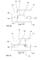
- FIGS. 1A to 1C shows an example of a substrate 100 in which a MOS transistor structure with an LDD region is to be produced.
- a source region 102 is schematically shown in the substrate 100, in which the source of the MOS transistor is to be generated during manufacture.
- an LDD area 104 is shown schematically, which is to be generated in subsequent process steps.
- a gate structure 108 is arranged on a surface 106 of the substrate 100, adjacent to which the source region 102 or the LDD region 104 is to be produced.
- the gate structure 108 has a minimum dimension x gate , which is given by the minimum structure width that can be achieved by the lithography.
- the minimum structure sizes used in production with today's lithography processes are approximately in the range of 0.2 ⁇ m.
- the separation between the source area 102 and the LDD area to ensure 104 is a photo technology Paint mask generated, its ideal arrangement in Fig. 1A at 110 is shown.
- the paint mask 110 has an edge 112 that is on the gate structure 108 is arranged so that the LDD area is completely covered by the mask 110, so during a subsequent processing of the source area 102, such as for example an implantation (see arrows 114) Avoid simultaneous editing of the LDD area becomes.
- 1B shows the situation in which the actual Edge 116 of the photomask 110 due to the adjustment tolerances no longer on the gate structure 108 but on the surface 106 of the substrate 100 in the region of the source region 102 lies, so that a portion 118 of the Source area 102 is masked.
- this masked section 118 is the source area during a subsequent one Processing masked, so that in the source area 102 an implantation 114 takes place, but not up to the Gate 108 is approaching.
- 1C shows the situation when the actual Edge 116 of the photomask 110 due to the adjustment tolerances is no longer located on the gate structure 108, but on the surface 106 in the region of the LDD region 104 of the substrate is arranged. This will make an area 120 of the LDD area, so that in a subsequent, process step actually reserved for the source area 102, This area 120 is also processed in the LDD area 102 so that, for example, an implantation is also possible here to create a highly doped area will, so reliable manufacture of the MOS transistor with LDD area is not guaranteed.
- a minimal gate length is desirable to e.g. to minimize the gate capacity. Furthermore, a minimal gate length has advantageous effects on the properties of the transistor, e.g. on the Slope, cutoff frequency etc.
- the present Invention the object of an improved method adjacent to the definition of a substrate area to be exposed to create a structure with which a structure with minimal structure width can be realized.
- the method relates to the manufacture of a MOS transistor with an LDD area, with the inventive method during the implantation steps the above-mentioned separation between the source area and the LDD area can be ensured at the same time Reaching a gate width equal to the minimum structure width that is achievable with the exposure process is, so with the same equipment that for those in the state manufacturing steps used in technology shorter gates can be generated.
- a so-called hard mask is generated, which is a source-side Implantation and a drainage-side implantation separates.
- the hard mask is preferably selective to those below Layer and selectively to the gate using a isotropic etching step can be etched.
- the advantage of the present invention is that a minimum gate width can now be achieved because the hard mask is generated on the substrate without adjustment tolerances and selective to the other materials of the substrate and the Gate structure is removable.
- the present invention is preferably applied to MOS transistors which have a lightly doped drain region between the gate structure and the actual drain region, this LDD region being larger than a region which can be produced by a spacer technology.
- a short LDD area can be generated by the spacer technology, but this occurs on the source and drain side of the gate structure.
- These LDD areas are required for MOS transistors that have to withstand high voltages.
- the method according to the invention is also used in LDMOS transistors with LDD areas.
- LDMOS transistors are MOS transistors with a laterally diffused channel region.
- the lightly doped drain region can either be implanted, for example by introducing an n-type implant into a p-type substrate, or formed by a grown n-epitaxial layer.
- the transistors with an implanted n-type region are mostly used in the HF range, the low-doped region being usually implanted with a dose of approximately 1 ⁇ 10 12 1 / cm 2 in order to increase the breakdown voltage.
- the transistors with an n-epitaxial layer are predominant used in the field of power transistors.
- the length of the LDD area located on one side of the gate is not about the photo technology conventional in the prior art determined, but using the invention Procedure, so the length of the LDD area is not is more subject to fluctuations in photo technology, so that the associated fluctuations in electrical Parameters of the LDMOS transistor can be reduced.
- the gate structure with a minimal structure width is according to this embodiment on later Another transition from the LDD area to the drain area Structure, for example a polystructure.
- This Structure has a minimum width and between the gate structure and the drain adjustment structure, as well as over the remaining
- the masking layer extends in the drain region. at In this embodiment, the masking layer is over the drain area to be created with the one described above, inventive method up to the additional polystructure removed. Then the drain implantation takes place, so that the distance of the drain area to the gate and hence the length of the LDD area by the one just described Etching is defined.
- the advantage of this approach is that there are no adjustment tolerances to the gate, because the gate as the first structure and the drain adjustment structure are generated together so that the state of the art Adjustment problems occurring when using the technology Photo technology can be avoided.
- the Polystructure remain and as a draining-side potential plate serve, but it can also be used with a suitable one Etching step are removed, the area in this etching step is defined with a photo technique.
- the LDD area was already before generating the structures on the substrate surface. However, the LDD area only becomes available after generation of the structures implanted, the masking layer must first be used for this above the LDD area.
- the further structure is formed in such a way that these form the entire Drain area covered, so that only between the gate and the Drain adjustment structure the masking layer remains.
- the polysilicon structure is completely over removed the drain area, here the paint level / paint edge on the adjacent masking layer section is provided that the etching process of the polysilicon is sufficient Selectivity to the material of the masking layer, z. B. oxide. Then the drain implantation takes place, so that here too the distance of the drain area to the gate and so that the length of the LDD region is defined by the etching step is, which also avoids the adjustment tolerances here become.
- the distance from gate to drain only through gate photo technology is determined by means of the structures in the gate and drain area be generated.
- the photo technique for creating the two Structures are well mastered, and in essence simultaneous production of the drain structure and the gate structure the distance between them can be adjusted very well. This will cause fluctuations in the distance between Gate area and drain area influenced electrical Parameters avoided.
- the method just described can also be used for self-adjustment Definition of a drain contact can be used, where for this purpose, a remaining gate oxide is etched away in the drain region becomes. At the same time, in this case, the oxide in the source area be removed so that the source contact up to the gate reaches.
- a distance between Self-adjusted gate and source contact such a source-side resistance at Power LDMOS transistors are used in the HF range.
- the procedure is similar to the exemplary embodiment described above, where another structure in the drain area is arranged. Again, another structure spaced from the gate area, on the future source area arranged, for example a polysilicon structure. After structuring the gate, it is removed, creating a desired distance in front of the gate with a Oxide nitride layer is covered, but the source area only is covered with a gate oxide. This is selectively removed so that a position of the source contact as well self-adjusted to the gate.
- Embodiment for producing an LDMOS transistor described with LDD range which the inventive Method used to expose a substrate area.
- Based 2A-2K are the individual steps for manufacturing of the LDMOS transistor explained in more detail.
- a structure in which a gate structure already exists is formed on a substrate.
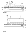
- 2A is a p-type substrate 200 shown, on which a p-epitaxial layer 202 is deposited has been.
- the epitaxial layer 202 On the surface facing away from the substrate 200 the epitaxial layer 202 is a first oxide layer 204 educated.
- the side walls of the gate polysilicon section 208 are also covered with oxide layers 212.
- etch stop layer 214 for example a thin nitride layer, deposited. That is on the nitride layer 214 Hard mask 216 formed, which is made of an oxide layer is. As can be seen from Fig. 2A, was on both sides the gate structure 206, the layer 216 applied, the gapless reaches gate 206, but through gate 206 is interrupted. Between gate structure 206 and the hard mask 216 are the nitride layer 214 and the oxide layer 212 arranged.
- an upper edge 218 of the hard mask 216 not with an upper edge 220 of the gate structure 206 must match.
- the hard mask 216 is produced by applying the thin nitride layer 214 as an etch stop to the surface of the oxide layer 204 and to the side oxide layers 212 and then depositing an oxide layer.
- the lowest point of the deposited oxide layer surface is in this case above the upper edge 220 of the gate polysilicon portion 208 of the gate structure 206.
- a lacquer layer for example applied a layer of photoresist, and then becomes an edge of the photoresist layer in one Target position determined photolithographically.
- the target position is over at least one adjustment tolerance of an exposure process from one edge of the gate structure to one that cannot be removed Section of the hard mask is adjacent, spaced to to get an actual position of the edge of the photoresist layer, either above the gate structure or above the to removing section of the hard mask.
- the hard mask etched around it to the gate structure to remove. 2B is the semiconductor structure known from FIG.
- Lacquer layer (photoresist layer) 222 was applied, the was structured such that its actual edge 224 something in the source area of the LDMOS structure to be created reaches in the embodiment described in FIG. 2 in the figures to the left of gate structure 206 is arranged.
- the actual edge 224 the lacquer layer 222 also with the source-side edge of the gate structure 206 complete or arranged on the gate structure if it is ensured that adjustment tolerances when creating edge 224 does not cause this in a drain-side area of the LDMOS semiconductor structure to be produced are arranged, which at the in Fig. 2nd described embodiments to the right of the gate structure 206 is arranged.
- 2C shows the semiconductor structure after completion of the Etching hard mask 216, and as can be seen, is area of the hard mask 216 completely up to gate structure 206 away. This isotropic etching became the layer on the source side up to the gate away. To do this, a material must be selected for layer 216 be a suitable selectivity to those areas has to be preserved. Alternative is it is also possible to use thin layers, such as the etch stop layer 214 between the areas to be protected and layer 216, layer 214 being an appropriate one Has selectivity.
- the paint layer is removed so that the 2D structure results.
- the channel material through an implantation of p-material, as shown by the arrows in Fig. 2D , the hard mask 216 in the drain region (in FIG. to the right of the gate structure 206) serves as a hard mask.
- the preparations for the generation of a so-called drain buffer carried out.
- the drain area is created using photo technology fixed and in the area of the later drain connection etched.
- An n-material is then implanted with a doping that is between a doping the drain implantation to be created and the one to be created LDD area.
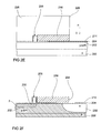
- 2E is the semiconductor structure shown on which another structured lacquer layer 226 is arranged, the edge 228 of the exposed Defined area of the drain connection in which after the Structuring the lacquer layer 226 the hard mask 216 in the exposed Area of the drain connection, preferably anisotropic is etched.
- the necessary implants are then implanted Doping as shown by the arrows in Fig.
- FIG. 2E is to use the drain buffer in a later step a doping between the doping of the LDD region and the doping of the future drain implantation area lies to generate. As can be seen from Fig. 2E, is for this implantation in the area of the drain connection is the source area covered with the photoresist 226. After implantation the photoresist 226 is removed.
- a temperature step is then carried out to determine the p-implantation in the source area under the gate structure 206 to drive the threshold voltage of the to be manufactured LDMOS transistor set.
- the drain buffer implantation performed in the previous step under hard mask 216.
- the resulting structure is shown in Fig. 2F.
- the p range diffused under the gate structure 206 to there the to form p-channel region 230.
- the drain buffer was also 232 generated, starting from an edge 234 of the hard mask 216 in the area of the future drain connection below the hard mask 216 extends.
- a subsequent step another layer of photoresist applied to the substrate, and an edge of this Photoresist layer is photolithographically in one Target position determined, this target position by at least one Adjustment tolerance of an exposure process from an edge the gate structure is spaced apart from a portion of the Hard mask adjacent between the gate structure and the source region, around an actual position of the edge of the photoresist layer get that either above the gate structure or above the portion of the masking layer between the gate structure and the drain area. Then follows etching the exposed portions of layer 216. In Fig. 2H is during a first anisotropic etching step setting structure shown.
- a photo layer 242 was applied, which is structured in this way was that an edge 244 of the same on the masking layer 216 is arranged.
- the distance of the edge 244 has been set up to ensure that the edge even with the minimum width of the gate structure 206 244 on gate 206 or, as shown, on layer 216 is arranged so that the source-side areas of the Structure securely covered by photoresist layer 242 are.
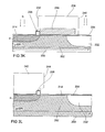
- Fig. 2H the situation is after an initial one anisotropic etching step in which part of the Layer 216 was removed. Another, isotropic The etch step, layer 216 becomes complete until the gate structure 206 away so that the one shown in FIG. 2I Semiconductor structure results.
- the photo layer 242 is then removed and the LDD region is implanted over the entire area.
- the required n-doping for the LDD region is introduced into the region between the gate structure 206 and the drain buffer 232.
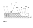
- the semiconductor structure produced in this way is then healed, so that the structure shown in FIG. 2J results.
- the source, LDD and drain regions are formed by the annealing step. As can be seen in FIG. 2J, the n + source area 246, the n-LDD area 248 and the n + drain area 250 were generated by the annealing.
- the already created drain buffer 232 is arranged between the drain region 250 and the LDD region 248.
- FIG. 2J completed semiconductor structure, and in This structure is shown in FIG. 2K, in which, compared 2J, the source region 246 a silicide contact 252, gate structure 206 a silicide surface 254, and the drain 250 comprises a silicide surface 256.
- the p-substrate 200 is doped with approximately 5 ⁇ 10 18 1 / cm 3
- the p-epitaxial layer 202 is doped in the range of 1.5 ⁇ 10 15 1 / cm 3 .
- the diffusion of the p-implantation introduced in the source region leads to p-doping in the source region and in the channel region which is between 10 15 and 10 18 1 / cm 3 .
- the implantation in the drain area and the diffusion of the drain buffer result in an n-doping in this area between 10 15 and 10 19 1 / cm 3 .
- the final annealing of the semiconductor structure leads to p-doping in the source region in the range from approximately 10 19 to 10 20 1 / cm 3 .
- the n-doping is in the range from 10 15 to 10 16 1 / cm 3 .
- the n-doping in the drain buffer is between 10 15 and 10 19 1 / cm 3 , and the drain has a doping in the range 10 19 to 10 20 1 / cm 3 .
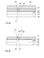
- a further exemplary embodiment is described below with reference to FIG. 3 described for the manufacture of an LDMOS transistor, which the inventive method for exposing a Includes substrate area.
- FIG. 3A shows a p-substrate 200, on which a p-epitaxial layer 202 is applied.
- An oxide layer 204 was applied to the exposed surface of the p-epitaxial layer 202, on which a thin silicon nitride layer 214 was applied.
- the masking layer 216 for example an SiO 2 layer, was applied to the exposed surface of the silicon nitride layer 214.
- a trench 258 has been etched into the masking layer or hard mask 216, which extends from the exposed surface of the hard mask 216 to the nitride layer 214.
- a subsequent, optional step can be provided be to deposit another nitride layer, so the selectivity to improve in later etching processes.
- FIG. 3B another thin nitride layer 260 is shown that is on the exposed surface of the masking layer 216 the side walls of the trench 258 as well as on that through the trench 258 exposed nitride layer 214 is arranged.
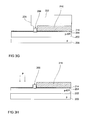
- the subsequent anisotropic etching step is the one in FIG. 3B shown another thin nitride layer 260 on the substrate facing surface of the masking layer 216 and in Bottom region of trench 258 removed.
- the etching step becomes the oxide layer 204 and the nitride layer at the same time 214 in the area of the bottom of the trench 256, so that the trench from the now exposed surface the masking layer 216 to the p-epitaxial layer 202 is sufficient, as shown in Fig. 3C.
- On the side walls of the trench 258 is the further thin one Nitride layer 260 obtained due to the anisotropic etching process remained.
- 3D is the resultant Structure shown after thermal oxidation, and in the bottom region of the trench 258 there is the gate oxide section 210 formed.
- the gate material 262 e.g. B. polysilicon on the surface of the in Fig. 3D structure shown deposited so that the trench is completely filled out.
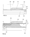
- gate material 262 is then etched back, so that 3F, the gate material is still in the trench 258 as gate material section 208, e.g. B. polysilicon, is available.
- gate material section 208 e.g. B. polysilicon
- the surface of the surface facing away from the substrate Hard mask 216 must be completely exposed, it may be no gate material 262 after the etching step are located. To achieve this, it is necessary that the etching process etches hard mask 216 more severely than that Gate material 262.
- the gate structure 206 shown in FIG. 3F was formed, essentially the gate structure shown in FIG. 2A equivalent.
- the LDD area be implanted before the gate structure is generated.
- the method according to the invention provided separation is still required to avoid that the weakly doped LDD region during a source implantation and a channel implantation is doped higher than is desired.
- the gate oxide (see Fig. 3D) and before deposition an oxide layer is deposited on the gate material (see FIG. 3E), which is then anisotropically etched back.
- This 4 results in trench 258 as shown in FIG so-called spacers 264 are generated.
- These spacers 264 effect in the subsequent step of applying the polysilicon 262 and the corresponding etching back of the same that the gate length, that is to say that lying under the gate material 208
- the area of the gate oxide 210 is shorter than the lithographic Length.
- the pre-formed thin nitride layer 260, the Protect remains on the walls of the trench 258 the spacers 264 during the isotropic etching steps the hard mask 216.
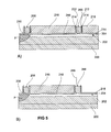
- FIGS. 5 to 7 is assumed to have a structure similar to is that shown in Fig. 2D and Fig. 3H, respectively.
- a structure is shown here in which the LDD area implanted before the gate structure is created has been.
- a procedure can also be used here can be selected as they are based on FIG. 2 and 3, namely the creation of the LDD area towards the end of the manufacturing process.
- a structure is similar to the structure shown in Figs. 2D and 3H, with the difference another structure 266 is shown, which follows is also referred to as a drain adjustment structure.
- the embodiment shown in FIG. 5 is the drain adjustment structure essentially identical to the gate structure 206 and also preferably consists of a polysilicon material. They are similar to gate structure 206 Sidewalls of the polysilicon material of the drain adjustment structure 266 covered with oxide layers 212, on which in turn Portions of the nitride layer 214 are arranged. Across from of epitaxial layer 202 is structure 266 through that Oxide layer 204 separated. As can also be seen in FIG.
- 5A was here before the masking layer was created 216 and structures 206 and 266 the LDD area 248 implanted. In contrast to those shown in Figs. 2D and 3H Situations, here becomes the masking layer 216 interrupted by the further structure 266, so that between gate structure 206 and drain adjustment structure 266 the first section of the masking layer 216 is arranged, and the remaining drain area through a second section masking layer 216 is covered.
- the structure 266 is from the layer sequence 212, 214 (oxide / nitride) Masking layer 216 separated.
- the manufacture 206 and 266 takes place on the basis of FIG. 2 described manner, that is, before the application of the masking layer 216, which according to an example after generation of structures 206 and 266 is applied to a The manner that has been described with reference to FIG. 2A.
- alternative structures 206 and 266 can be based on the 3 described in the masking layer become.
- the advantage of this approach is that the Structures 206 or 266 with a common photostructuring process are generated by means of which the distance between gate structure 206 and drain adjustment structure 266 can be adjusted well. This allows for another Photo technology for determining the edge of the masking layer on the drainage side 216 can be dispensed with, thereby simultaneously the adjustment tolerances associated with this definition of the edge be avoided.
- This etching step takes place using a photo technique by means of which between the gate structure 206 and the adjustment structure 266 lying section of the masking layer 216 and the source region of the structure to be created.
- the photoresist edge is adjusted in the same way and Way, above in connection with the generation of the gate structure 206 has been described. More specifically, one will Edge, which is indicated by dashed lines at 268 in FIG.
- an adjustment tolerance of the exposure method used spaced from the edge of the adjustment structure 266 is that of the portion of the masking layer to be removed is spaced so as to provide an actual position of the edge 268 get that either above the adjustment structure or above the portion of the masking structure to be removed lies.
- Fig. 5B The structure resulting after the etching step is shown in Fig. 5B. As can be seen, here is the future one Drain region, to the right of the further structure 266 in FIG. 5B exposed. Only the oxide layer 204 and the nitride layer 216 are available there.
- the Embodiment according to FIG. 5C the edge of the implantation area no longer defined by the photoresist edge 228, but through structure 266. As mentioned above was, this is the structure of the Photoresist layer 226 inherent adjustment tolerances and thus the uncertainty in the arrangement of the drain area avoided. It is sufficient if the one shown in Fig.
- Embodiment of the source area is safely covered, and edge 228 anywhere on the structures 206 and 266 or arranged on the masking layer 216 is, which in each case as a mask against an implantation of n material in the areas below.
- the Implantation is indicated by the arrows in FIG. 5C.
- 5D shows the situation that arises after the implanted material is driven out to the To generate drain buffer 232. This sprouting happens like already described above, for example, by a temperature step, through which a diffusion of the inserted drain buffer implantation done under the hard mask as it is in 5D is shown.
- Embodiment assumed a situation at the one before structuring the drain area Diffusion of the p-region under the gate structure 206 performed has been. Alternatively, this can be done, as in the case of the 2 and 3 described embodiment, also together with the diffusion of the drain buffer.
- the structure shown in Fig. 5D essentially corresponds the structure shown in FIG. 2F or in FIG. 3J, except for the fact that in Fig. 5 still the structure 266 is present.
- This structure 266 may, in one embodiment be removed in another embodiment can be used as a potential plate over the transition from LDD area to drain area remain. The removal of the Structure 266 is accomplished using common etching techniques a photo technique to cover the remaining area protect.
- the LDMOS transistor is processed to the end, corresponding to the process steps with reference to FIG. 2G to 2K or 3K to 3N have been described.
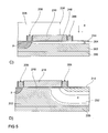
- FIG. 6A differs from that described with reference to FIG. 5A differs in that the drain adjustment structure 266 is designed such that it covers the entire future Drain area covered.
- This layer is preferably formed by a polysilicon.
- the masking layer 216 is arranged, and the same is over an oxide layer 212 as well a nitride layer 214 is separated from the further structure 266.
- the further structure 266 is through the oxide layer 204 separated from underlying layers.
- FIG. 6B shows the situation in which the already 2E known photo layer 226 on the source region, on gate 206 as well as on a portion of the masking layer 216 is arranged.
- the drain area over the edge 228 of the resist layer 226 is determined because of the selective etching the material of structure 266 does not etch the masking layer 216 is done so that the edge 228 just on masking layer 216 as shown in FIG. 6 is shown.
- the photoresist 226 is then removed and the drain buffer is diffused out, so that the one shown in FIG. 6C Structure that is similar to the structure as shown in Figures 2F and 3J, respectively.
- the drain region to be generated directly adjacent to the edge of the drain buffer can be used for the following implantation the source and drain areas are made without an additional mask, whereby the drain implantation as well as the insertion of the drain buffer material is self-adjusted. Is a Distance of the implantations from the drain buffer edge desired, so must on the photo technology described with reference to Fig. 2G be used.
- Embodiments of the method also for self-adjusted Definition of a drain contact can be used that is, the distance between a metal contact to be generated and the connection the drain area.
- the drain area oxide layer 204 and nitride layer 214 respectively the oxide layer 204 (exemplary embodiment according to FIG. 6) removed, and a corresponding contacting of the drain area is brought about.
- the oxide layer 204 and / or nitride layer 214 are removed in the source region, and a corresponding contact for the source connection is established become.
- the drain contact is more defined Distance from the gate and the source contact is sufficient up to the gate.
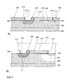
- FIG. 7A An example of a structure that is similar is shown in FIG. 7A to that in Fig. 6A, however, the illustration is further the source area (in the figure to the left of the Gate structure 206).
- source adjustment structure 270 shown, spaced from gate 206 above a source region to be generated is arranged.
- Structure 270 is similar to the other structures for example made of polysilicon and is opposite to the one below Substrate area isolated by the oxide layer 204. From one already in FIG. 7A by the inventive one Removed masking layer, this was through the oxide layer 214 and a further oxide layer 212 are insulated, similar to structure 266 of section 216 of FIG Masking layer.
- Structure 270 becomes common with the remaining structures 206 and 266 or only with the Structure 206 provided there is only an appropriate distance between Source and gate is desired, which produces what is mentioned above was, together with the gate manufacturing with high accuracy can be done.
- structural shape 270 a structural shape similar to that chosen 5A in connection with the drain adjustment structure 266 has been described.
- the structure 270 is removed, the remaining areas of the substrate with a Photoresist layer 272 are covered to prevent unwanted etching avoid other parts.
- the one shown in Fig. 7B Example is assumed that the removal of the Drain adjustment structure 266 is done, as is the diffusion the drain buffer implantation.
- the edge 274 of the Photoresist layer 272 is set to be on the polysilicon structure 270 is arranged.
- Fig. 7C The resulting structure is shown in Fig. 7C.
- the oxide layer 204 in the Area etched in which the same is not through the nitride layer 214 is protected. In the areas exposed as a result of the source section or the drain section then the metallic contact.
- the inventive method in general can be used in situations in which areas of a Substrate adjacent to a structure while maintaining minimal Structure sizes need to be edited, with others Areas adjacent to the structure must be protected.
- the production of LDMOS transistors takes place the present Invention also applied to MOS transistors with LDD range.
Landscapes
- Insulated Gate Type Field-Effect Transistor (AREA)
Abstract
Description
- 100
- Substrat
- 102
- Sourcebereich
- 104
- LDD-Bereich
- 106
- Oberfläche
- 108
- Gatestruktur
- 110
- Photoresistschicht
- 112
- Kante der Photoresistschicht 110
- 114
- Implantation
- 116
- Ist-Kante der Photoresistschicht 110
- 118
- maskierter Abschnitt des Sourcebereichs 102
- 120
- freigelegter Abschnitt des LDD-Bereichs 104
- 200
- Substrat
- 202
- Epitaxieschicht
- 204
- erste Oxidschicht
- 206
- Gatestruktur
- 208
- Gatepolysiliziumabschnitt
- 210
- Gateoxidabschnitt
- 212
- weitere Oxidschicht
- 214
- Ätzstoppschicht
- 216
- Hartmaske
- 218
- Oberkante der Hartmaske
- 220
- Oberkante der Gatestruktur 206
- 222
- Photoresistschicht
- 224
- Kante der Photoresistschicht 222
- 226
- Photoresistschicht
- 228
- Kante der Photoresistschicht 226
- 230
- Kanalbereich
- 232
- Drainpuffer
- 234
- Kante der Hartmaske 216
- 236
- Photoresistschicht
- 238
- erste Kante der Photoresistschicht 236
- 240
- zweite Kante der Photoresistschicht 236
- 242
- Photoresistschicht
- 244
- Kante der Photoresistschicht 242
- 246
- n+-Source
- 248
- n-LDD-Bereich
- 250
- n+-Drain
- 252-256
- Aluminiumanschlussflächen
- 258
- Graben
- 260
- Nitridschicht
- 262
- Gatematerial
- 264
- Spacer
- 266
- Drain-Justage-Struktur
- 268
- Photoresistkante
- 270
- Source-Justage-Struktur
- 272
- Photoresistschicht
- 274
- Kante der Photoresistschicht 272
Claims (22)
- Verfahren zum photolithographischen Festlegen eines freigelegten Substratbereichs, der direkt an eine auf dem Substrat (200, 202) angeordnete Struktur (206; 266; 270) angrenzt, mit folgenden Schritten:(a) Aufbringen einer Maskierungsschicht (216), die bis an die Struktur (206; 266; 270) heranreicht, auf dem Substrat (200, 202);(b) Aufbringen einer Photoresistschicht (222);(c) photolithographisches Festlegen einer Kante (224) der Photoresistschicht (222) in einer Solllage, die um mindestens eine Justagetoleranz eines Belichtungsverfahrens von einer Kante der Struktur (206; 266; 270) beabstandet ist, die an einen nicht zu entfernenden Abschnitt der Maskierungsschicht (216) angrenzt, um eine Istlage der Kante (224) der Photoresistschicht (222) zu erhalten, die entweder oberhalb der Struktur (206; 266; 270) oder oberhalb des zu entfernenden Abschnitts der Maskierungsschicht (216) liegt; und(d) Ätzen der Maskierungsschicht (216) unter Verwendung der im Schritt (c) strukturierten Photoresistschicht (222), um die Maskierungsschicht (216) bis zu der Struktur (206; 266; 270) zu entfernen.
- Verfahren nach Anspruch 1, mit folgendem Schritt vor dem Schritt (a):Bereitstellen des Substrats (200, 202), wobei die Struktur (206; 266; 270) auf einer Oberfläche des Substrats (200, 202) gebildet ist.
- Verfahren nach Anspruch 1, bei dem der Schritt (a) folgende Teilschritte umfasst:(a.1) Aufbringen der Maskierungsschicht (216) auf einer Oberfläche des Substrats (200, 202);(a.2) Bilden einer Ausnehmung (258) in der Maskierungsschicht (216), die von einer dem Substrat (200, 202) abgewandten Oberfläche der Maskierungsschicht (216) bis zu der Oberfläche des Substrats (200, 202) reicht; und(a.3) Einbringen eines ausgewählten Materials (208, 210) in die Ausnehmung (258), um die Struktur (206; 266; 270) zu bilden.
- Verfahren nach Anspruch 3, bei dem die Ausnehmung (258) die kleinste, lithographisch erreichbare Abmessung hat, und bei der der Schritt (a.3) folgende Schritte umfasst:Bilden einer Beabstandungsschicht (264) an den Wänden der Ausnehmung (258); undEinbringen des Strukturmaterials (262), um eine Struktur (206; 266; 270) mit einer Abmessung zu bilden, die kleiner ist als die kleinste lithographisch erreichbare Abmessung.
- Verfahren nach einem der Ansprüche 1 bis 4, bei dem die Maskierungsschicht (216) aus einem Material gebildet ist, das bezüglich dem Substratmaterial und bezüglich dem Strukturmaterial selektiv ätzbar ist.
- Verfahren nach einem der Ansprüche 1 bis 5, bei dem zwischen dem Substrat (200, 202) und der Maskierungsschicht (216) und/oder zwischen der Struktur (206; 266; 270) und der Maskierungsschicht (216) eine Ätzstoppschicht (214, 260) angeordnet ist.
- Verfahren nach einem der Ansprüche 1 bis 6, bei dem der Schritt (d) ein isotropes und/oder anisotropes Ätzen umfasst.
- Verfahren nach einem der Ansprüche 1 bis 7, bei dem die auf dem Substrat (200, 202) angeordnete Struktur ein Gate (206) eines MOS-Transistors ist, und bei dem der freigelegte Substratbereich einen Sourcebereich des MOS-Transistors in dem Substrat (200, 202) definiert.
- Verfahren nach einem der Ansprüche 1 bis 7, bei dem die auf dem Substrat (200, 202) angeordnete Struktur eine Drain-Justage-Struktur (266) ist, die an einem Übergang eines LDD-Bereichs oder Resurf-Bereichs (248) zu einem Drainbereich (250) eines LDMOS-Transistors angeordnet ist, wobei der freigelegte Substratbereich der Drainbereich (250) des MOS-Transistors ist.
- Verfahren nach Anspruch 8, das ferner folgende Schritte umfasst:(e) photolithographisches Freilegen eines Substratbereichs, der von der Maskierungsschicht (216) bedeckt und von dem Gate (206) beabstandet ist, um einen Drainbereich des MOS-Transistors in dem Substrat (200, 202) zu definieren;(f) Erzeugen der Source (246) des MOS-Transistors und der Drain (250) des MOS-Transistors in dem Sourcebereich bzw. in dem Drainbereich in dem Substrat (200, 202);(g) photolithographisches Festlegen einer weiteren Kante (244) der Photoresistschicht (242) in einer Solllage, die um eine Justagetoleranz eines Belichtungsverfahrens von einer weiteren Kante des Gates (206) beabstandet ist, die an einen Abschnitt der Maskierungsschicht (216) zwischen dem Gate (206) und der Source (246) angrenzt, um eine Istlage der Kante (244) der Photoresistschicht (242) zu erhalten, die entweder oberhalb des Gates (206) oder oberhalb des Abschnitts der Maskierungsschicht (216) zwischen dem Gate (206) und der Drain (250) liegt; und(h) Ätzen der Maskierungsschicht (216) unter Verwendung der im Schritt (g) strukturierten Photoresistschicht (242), um die Maskierungsschicht (216) bis zu dem Gate (206) zu entfernen; und(i) Erzeugen einer leicht dotierten Drain (248) in dem Substrat (200, 202), zwischen dem Gate (206) und der Drain (250).
- Verfahren nach Anspruch 10, mit folgenden Schritten vor dem Schritt (e)
Entfernen der Photoresistschicht (222);
Einbringen einer Implantation zur Erzeugung eines lateral diffundierten Kanals in den Sourcebereich; und
Aufbringen einer weiteren Photoresistschicht (226);
wobei das Verfahren folgende Schritte zwischen dem Schritt (e) und dem Schritt (f) umfasst:wobei nach dem Schritt (f) die Photoresistschicht (236) entfernt wird und eine neue Photoresistschicht (242) vollständig auf die Oberfläche aufgebracht wird.Einbringen einer Implantation zur Erzeugung eines Drainbereichs, dessen Dotierungskonzentration zwischen der Drainkontaktimplantation und der LDD-Implantation liegt (Drainbuffer) ;Eindiffundieren der in den Sourcebereich eingebrachten Implantation unter das Gate (206) und Eindiffundieren der in den Drainbereich angebrachten Implantation unter die angrenzende Maskierungsschicht (216); undAbdecken der Maskierungsschicht (216) zwischen dem Gate (206) und der Drain (250) mittels einer Photoresistschicht (236); - Verfahren nach Anspruch 8, bei dem auf dem Substrat (200; 202) eine weitere Struktur (266) angeordnet ist, die eine Drain-Justage-Struktur ist, die an einem Übergang des LDD-Bereichs (248) zu dem Drainbereich (250) des LDD-MOS-Transistors angeordnet ist, wobei ein Abschnitt der Maskierungsschicht (216) zwischen dem Gate (206) und der Drain-Justage-Struktur (266) angeordnet ist, mit folgenden Schritten:(e) photolithographisches Festlegen einer Kante (268) einer Photoresistschicht, die das Gate und die Maskierungsschicht bedeckt, in der Solllage, die um mindestens eine Justagetoleranz eines Belichtungsverfahrens von einer Kante der weiteren Struktur (266) beabstandet ist, die an einen nicht zu entfernenden Abschnitt der Maskierungsschicht (216) angrenzt, um eine Istlage der Kante (268) der Photoresistschicht zu erhalten, die entweder oberhalb der weiteren Struktur (266) oder oberhalb des zu entfernenden Abschnitts der Maskierungsschicht (216) liegt;(f) Ätzen der Maskierungsschicht (216) unter Verwendung der im Schritt (e) strukturierten Photoresistschicht, um die Maskierungsschicht (216) zu der weiteren Struktur (266) zu entfernen, um den Drainbereich freizulegen; und(g) Erzeugen der Source (246) und der Drain (250) des MOS-Transistors in dem Substrat (200, 202).
- Verfahren nach Anspruch 13, bei dem der LDD-Bereich (248) des MOS-Transistors vor dem Erzeugen der Gatestruktur (206) und der Drain-Justage-Struktur (266) erzeugt wird, oder bei dem der LDD-Bereich (248) des MOS-Transistors zusammen mit der Source (246) und der Drain (250) erzeugt wird.
- Verfahren nach Anspruch 12 oder 13, mit folgenden Schritten nach dem Schritt (e):wobei das Verfahren folgende Schritte zwischen dem Schritt (f) und dem Schritt (g) umfasst:Entfernen der Photoresistschicht; undEinbringen einer Implantation zur Erzeugung eines lateral diffundierten Kanals in den Sourcebereich;Einbringen einer Implantation zur Erzeugung eines Drainbuffers (232) in dem Drainbereich; undEindiffundieren der in den Sourcebereich eingebrachten Implantation unter das Gate (206) und Eindiffundieren der in den Drainbereich eingebrachten Implantation unter die angrenzende Maskierungsschicht (216).
- Verfahren nach einem der Ansprüche 12 bis 14, bei dem die weitere Struktur (266) entfernt wird.
- Verfahren nach Anspruch 8, bei dem auf dem Substrat eine weitere Struktur (266) angeordnet ist, die einen Drainbereich (250) des MOS-Transistors bedeckt, wobei ein Abschnitt der Maskierungsschicht (216) zwischen dem Gate (206) und der weiteren Struktur (266) angeordnet ist, mit folgenden Schritten:(e) Entfernen der weiteren Struktur (266), um einen Drainbereich freizulegen; und(f) Erzeugen der Source (246) und der Drain (250) des MOS-Transistors in dem Substrat (200, 202).
- Verfahren nach Anspruch 15, bei dem der LDD-Bereich (248) des MOS-Transistors vor dem Erzeugen der Gatestruktur (206) und der Drain-Justage-Struktur (266) implantiert wird, oder bei dem der LDD-Bereich (248) des MOS-Transistors zusammen mit der Source (246) und der Drain implantiert wird.
- Verfahren nach Anspruch 16 oder 17 mit folgendem Schritt nach dem Schritt (e):wobei das Verfahren folgende Schritte zwischen dem Schritt (e) und dem Schritt (f) umfasst:Einbringen einer Implantation zur Erzeugung eines lateral diffundierten Kanals in den Sourcebereich;Einbringen einer Implantation zur Erzeugung eines Drainbuffers in dem Drainbereich; undEindiffundieren der in den Sourcebereich eingebrachten Implantation unter das Gate (206) und Eindiffundieren der in den Drainbereich eingebrachten Implantation unter die angrenzende Maskierungsschicht (216).
- Verfahren nach einem der Ansprüche 12 bis 18, bei dem die Struktur (206) und die weitere Struktur (266) gemeinsam erzeugt werden.
- Verfahren nach einem der Ansprüche 9 bis 19, bei dem die weitere Struktur (266) eine Position eines Drainkontakts (256) auf dem Substrat (200, 202) festlegt.
- Verfahren nach einem der Ansprüche 8 bis 20, bei dem auf dem Substrat (200, 202) eine dritte Struktur (270) angeordnet ist, die beabstandet zu dem Gate (206) angeordnet ist und einen Sourcebereich des MOS-Transistors zumindest teilweise bedeckt, um eine Position eines Sourcekontakts (252), der beabstandet von dem Gate (206) angeordnet wird, festzulegen.
- Verfahren nach einem der Ansprüche 8 bis 21, mit folgenden Schritten:Ausheilen der erzeugten Halbleiterstruktur; undAufbringen von metallischen Anschlussstellen (252, 254, 256) auf dem Gate (206), der Source (246) und der Drain (250), um den Gatekontakt, den Sourcekontakt und den Drainkontakt zu bilden.
Applications Claiming Priority (2)
| Application Number | Priority Date | Filing Date | Title |
|---|---|---|---|
| DE10149028 | 2001-10-05 | ||
| DE10149028A DE10149028A1 (de) | 2001-10-05 | 2001-10-05 | Verfahren zum photolithographischen Festlegen eines freigelegten Substratbereichs |
Publications (1)
| Publication Number | Publication Date |
|---|---|
| EP1300880A2 true EP1300880A2 (de) | 2003-04-09 |
Family
ID=7701414
Family Applications (1)
| Application Number | Title | Priority Date | Filing Date |
|---|---|---|---|
| EP02019495A Withdrawn EP1300880A2 (de) | 2001-10-05 | 2002-08-30 | Verfahren zum photolithographischen Festlegen eines freigelegten Substratbereichs |
Country Status (2)
| Country | Link |
|---|---|
| EP (1) | EP1300880A2 (de) |
| DE (1) | DE10149028A1 (de) |
Cited By (1)
| Publication number | Priority date | Publication date | Assignee | Title |
|---|---|---|---|---|
| WO2005017993A1 (en) * | 2003-08-04 | 2005-02-24 | Advanced Micro Devices, Inc. | Method for asymmetric sidewall spacer formation |
-
2001
- 2001-10-05 DE DE10149028A patent/DE10149028A1/de not_active Withdrawn
-
2002
- 2002-08-30 EP EP02019495A patent/EP1300880A2/de not_active Withdrawn
Cited By (3)
| Publication number | Priority date | Publication date | Assignee | Title |
|---|---|---|---|---|
| WO2005017993A1 (en) * | 2003-08-04 | 2005-02-24 | Advanced Micro Devices, Inc. | Method for asymmetric sidewall spacer formation |
| GB2421854A (en) * | 2003-08-04 | 2006-07-05 | Advanced Micro Devices Inc | Method of asymmetric sidewall spacer formation |
| GB2421854B (en) * | 2003-08-04 | 2007-01-24 | Advanced Micro Devices Inc | Method of asymmetric sidewall spacer formation |
Also Published As
| Publication number | Publication date |
|---|---|
| DE10149028A1 (de) | 2003-05-08 |
Similar Documents
| Publication | Publication Date | Title |
|---|---|---|
| DE4344285B4 (de) | Verfahren zur Herstellung eines Transistors | |
| DE4212829C2 (de) | Verfahren zur Herstellung von Metall-Oxid-Halbleiter-Feldeffekttransistoren | |
| DE69434643T2 (de) | Struktur und Herstellung von Leistungs-MOSFET unter Einbeziehung der Struktur des Randes | |
| DE112004000872B4 (de) | Anordnung eines Trench-MOSFETs mit Selbstausrichtungsmerkmalen | |
| DE10234392B4 (de) | Halbleiterbauelement mit Gate-Elektrodenstruktur und Herstellungsverfahren hierfür | |
| EP1204992B1 (de) | Verfahren zum herstellen eines trench-mos-leistungstransistors | |
| DE102012214077A1 (de) | Integrierte Schaltungen mit abstehenden Source- und Drainbereichen und Verfahren zum Bilden integrierter Schaltungen | |
| DE112010002352T5 (de) | FinFET-Strukturen mit verspannungsinduzierenden Source/Drain-biIdenden Abstandshaltern und Verfahren zur Herstellung der FinFET-Strukturen | |
| AT504289A2 (de) | Trench-gate-feldeffekttransistoren und verfahren zum bilden derselben | |
| DE10351008B4 (de) | Verfahren zur Herstellung von Transistoren mit erhöhten Drain- und Sourcegebieten mit unterschiedlicher Höhe sowie ein Halbleiterbauelement | |
| DE10131237A1 (de) | Feldeffekttrasistor und Verfahren zu seiner Herstellung | |
| DE19750221B4 (de) | Verfahren zu Herstellung eines Halbleiterbauteils mit MOS-Gatesteuerung | |
| DE10012112C2 (de) | Steg-Feldeffekttransistor und Verfahren zum Herstellen eines Steg-Feldeffekttransistors | |
| WO2004107435A1 (de) | Nrom-halbleiterspeichervorrichtung und herstellungsverfahren | |
| DE10262313B4 (de) | Verfahren zur Herstellung eines Halbleiterbauelementes und Halbleiterbauelement | |
| DE19543859A1 (de) | Transistor und Transistorherstellungsverfahren | |
| DE10012897B4 (de) | Transistor und Verfahren zu seiner Herstellung bzw. Hestellung einer Halbleitervorrichtung | |
| DE10261600B4 (de) | Halbleiterbauteil und Verfahren zu seiner Herstellung | |
| DE4207913C2 (de) | Metall-Oxid-Halbleiter-Feldeffekttransistoren und Verfahren zu ihrer Herstellung | |
| DE10215365B4 (de) | Transistorstruktur unter Verwendung von Epitaxialschichten und Verfahren zur Herstellung derselben | |
| DE69519016T2 (de) | Hochspannungs-ldd-mosfet mit erhöhter durchbruchspannung und herstellungsverfahren | |
| DE10341359B4 (de) | Halbleitervorrichtung und Verfahren zur Herstellung derselben | |
| DE19830543B4 (de) | Halbleitereinrichtung mit Hohlraum zwischen den Isolationsseitenwandstücken und dem Halbleitersubstrat und Verfahren zu ihrer Herstellung | |
| WO2015150268A1 (de) | Verfahren zur herstellung eines substrats, substrat, metall-oxid-halbleiter-feldeffekttransistor mit einem substrat und mikroelektromechanisches system mit einem substrat | |
| DE19742181B4 (de) | Herstellungsverfahren für eine Halbleitervorrichtung |
Legal Events
| Date | Code | Title | Description |
|---|---|---|---|
| PUAI | Public reference made under article 153(3) epc to a published international application that has entered the european phase |
Free format text: ORIGINAL CODE: 0009012 |
|
| 17P | Request for examination filed |
Effective date: 20020830 |
|
| AK | Designated contracting states |
Kind code of ref document: A2 Designated state(s): AT BE BG CH CY CZ DE DK EE ES FI FR GB GR IE IT LI LU MC NL PT SE SK TR Designated state(s): AT BE BG CH CY CZ DE DK EE ES FI FR GB GR IE IT LI LU MC NL PT SE SK TR |
|
| AX | Request for extension of the european patent |
Extension state: AL LT LV MK RO SI |
|
| STAA | Information on the status of an ep patent application or granted ep patent |
Free format text: STATUS: THE APPLICATION HAS BEEN WITHDRAWN |
|
| RIC1 | Information provided on ipc code assigned before grant |
Ipc: 7H 01L 21/28 B Ipc: 7H 01L 21/311 B Ipc: 7H 01L 29/78 B Ipc: 7H 01L 21/336 A |
|
| 18W | Application withdrawn |
Effective date: 20040507 |