EP1298672A2 - Circuit de réécriture de mémoire flash, circuit intégré à semiconducteurs, carte de mémoire ayant ce circuit intégré à semiconducteurs, méthode de réécriture de mémoire flash et programme de réécriture de mémoire flash - Google Patents
Circuit de réécriture de mémoire flash, circuit intégré à semiconducteurs, carte de mémoire ayant ce circuit intégré à semiconducteurs, méthode de réécriture de mémoire flash et programme de réécriture de mémoire flash Download PDFInfo
- Publication number
- EP1298672A2 EP1298672A2 EP02021375A EP02021375A EP1298672A2 EP 1298672 A2 EP1298672 A2 EP 1298672A2 EP 02021375 A EP02021375 A EP 02021375A EP 02021375 A EP02021375 A EP 02021375A EP 1298672 A2 EP1298672 A2 EP 1298672A2
- Authority
- EP
- European Patent Office
- Prior art keywords
- flash memory
- data
- circuit
- memory
- cpu
- Prior art date
- Legal status (The legal status is an assumption and is not a legal conclusion. Google has not performed a legal analysis and makes no representation as to the accuracy of the status listed.)
- Withdrawn
Links
Images


Classifications
-
- G—PHYSICS
- G11—INFORMATION STORAGE
- G11C—STATIC STORES
- G11C16/00—Erasable programmable read-only memories
- G11C16/02—Erasable programmable read-only memories electrically programmable
- G11C16/06—Auxiliary circuits, e.g. for writing into memory
-
- G—PHYSICS
- G11—INFORMATION STORAGE
- G11C—STATIC STORES
- G11C16/00—Erasable programmable read-only memories
- G11C16/02—Erasable programmable read-only memories electrically programmable
- G11C16/06—Auxiliary circuits, e.g. for writing into memory
- G11C16/10—Programming or data input circuits
- G11C16/102—External programming circuits, e.g. EPROM programmers; In-circuit programming or reprogramming; EPROM emulators
- G11C16/105—Circuits or methods for updating contents of nonvolatile memory, especially with 'security' features to ensure reliable replacement, i.e. preventing that old data is lost before new data is reliably written
-
- G—PHYSICS
- G11—INFORMATION STORAGE
- G11C—STATIC STORES
- G11C16/00—Erasable programmable read-only memories
- G11C16/02—Erasable programmable read-only memories electrically programmable
- G11C16/06—Auxiliary circuits, e.g. for writing into memory
- G11C16/10—Programming or data input circuits
- G11C16/102—External programming circuits, e.g. EPROM programmers; In-circuit programming or reprogramming; EPROM emulators
-
- G—PHYSICS
- G11—INFORMATION STORAGE
- G11C—STATIC STORES
- G11C16/00—Erasable programmable read-only memories
- G11C16/02—Erasable programmable read-only memories electrically programmable
- G11C16/06—Auxiliary circuits, e.g. for writing into memory
- G11C16/34—Determination of programming status, e.g. threshold voltage, overprogramming or underprogramming, retention
- G11C16/3436—Arrangements for verifying correct programming or erasure
- G11C16/3454—Arrangements for verifying correct programming or for detecting overprogrammed cells
- G11C16/3459—Circuits or methods to verify correct programming of nonvolatile memory cells
-
- G—PHYSICS
- G11—INFORMATION STORAGE
- G11C—STATIC STORES
- G11C2216/00—Indexing scheme relating to G11C16/00 and subgroups, for features not directly covered by these groups
- G11C2216/12—Reading and writing aspects of erasable programmable read-only memories
- G11C2216/16—Flash programming of all the cells in an array, sector or block simultaneously
Definitions
- the present invention relates to a method for rewriting information of a memory IC card, and more particularly relates to a flash memory rewrite circuit which is used in the case of rewriting information data using a flash memory IC card, a semiconductor integrated circuit for an memory IC card, a memory IC card, a flash memory rewriting method, and a flash memory rewriting program.
- Fig. 1 illustrates the structure of a large scale integrated device (LSI) 41 for an integrated circuit card (IC card) for general use.
- flash memory 14 serving as memory on LSI 41
- an EEPROM and the like may be used in place of the flash memory 14 as illustrated in Fig. 2.
- a CPU 11 designates data and an address for a designated byte for rewriting in EEPROM 17 via a bus 10. Since the designated byte for rewriting data is directly designated by the CPU 11, data can be rewritten for each designated byte.
- EEPROM 17 increases an area, EEPROM 17 cannot respond to the need for an increase in capacity in such a system that has a determined maximum chip area such as an IC card. Accordingly, EEPROM 17 is often used in an IC card of up to about 16 Kbytes.
- the LSI 41 using flash memory 14 as shown in Fig. 1 can respond to the need of an IC card up to about 128 Kbytes.
- the flash memory 14 generally performs rewriting per block, an operation must be carried out according to a special flow in order to perform rewriting for each designated byte.
- rewriting per byte can be carried out in one step but the capacity is small, while the flash memory can deal with the large capacity but needs several steps to perform rewriting per byte.
- data and an address for a designated byte for rewriting are directly designated, so that rewriting can be carried out in one step, while the byte rewriting of flash memory needs the plurality of steps as mentioned above.
- the program developers had to create an application with consideration given to the way of handling data for all bytes corresponding to one page including rewriting portions even when designated data with several bytes was stored.
- a flash memory rewrite circuit which is capable of rewriting a flash memory per byte, a semiconductor integrated circuit for a memory IC card having the flash memory rewrite circuit, a memory IC card, a flash memory rewriting method, and a flash memory rewriting program.
- a flash memory rewrite circuit including: a rewrite data control circuit, receiving a rewrite instruction of a flash memory from a CPU to store data for a designated byte of a page for rewriting to a memory block; a wait control circuit, generating and canceling a wait instruction to the CPU; a page data control circuit, sending data of the page excluding the designated byte to the memory block from the flash memory to prepare new page data in the memory block; and a data set control circuit that writes the new page data prepared in the memory block into the flash memory.
- a flash memory rewriting method including: receiving a rewrite instruction of a flash memory from a CPU; storing data for a designated byte of a page for rewriting to a memory block; generating a wait instruction to said CPU; sending data of said page excluding the designated byte to said memory block from said flash memory to prepare new page data in said memory block; setting said new page data prepared in said memory block at an page address of said flash memory; rewriting data of said flash memory; and canceling said wait instruction to said CPU.
- Fig. 5(a) is a schematic plane view illustrating a structure of a memory IC card according to an exemplary of the present invention.
- the IC card is a card mounting memory blocks (for example, EEPROM, FLASH MEMORY, DRAM, ROM, etc) and a control circuit on card substrate.
- the IC card is used, for example, a cash card, credit card, debit card, SIM (Subscribers Identity Module) card, USIM (Universal Subscribers Identity Module) card etc. Sometimes this type of card is called 'plastic'.
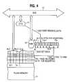
- An IC card 100 comprises a card substrate 90, an LSI 40 for an IC card mounted on the card substrate 90, a VDD terminal 61, a RST terminal 62, a CLK terminal 63, an I/O terminal 64, and a GND terminal 65. Moreover, substrate wirings 71 to 75 are formed on the card substrate 90.
- a CPU 11, a RAM 12, a ROM 13, a flash memory 14, a coprocessor 15, a RANDOM 16, and a flash memory rewrite circuit 1 are integrated on a semiconductor chip.
- a VDD terminal pad 21, a RST terminal pad 22, a CLK terminal pad 23, an I/O terminal pad24, and a GND terminal pad 25, which are bonding pads that respectively perform data exchange with terminals 61, 62, ..., 65, are arranged at the peripheral portion of the semiconductor chip.
- a spacer 91 is bonded to one surface side of the card substrate 90.
- the spacer 91 has a hollow portion to which the LSI 40 for an IC card is inserted, and the LSI 40 for an IC card is bonded to the card substrate 90 at the interior of the hollow portion of the spacer 91.
- IC card 100 both surfaces of the card substrate 90 having LSI 40 for an IC card mounted thereon are respectively covered with the upper cover film 92 and lower cover film 93 so as to sandwich spacer 91.
- Fig. 5(b) is one example of IC cards, and, of course, other structure may be used.
- CPU 11 performs control processing for providing a writing instruction to the flash memory rewrite circuit 1, and the like.
- RAM 12 is a memory for data processing.
- ROM 13 records a program, which is based on management definition, thereon.
- Flash memory 14 is nonvolatile memory, which can be electrically erased and rewritten per block, and which has larger capacity than EEPROM.
- Coprocessor 15 is a processor that handles an auxiliary function. A typical example for a coprocessor 15 is a floating point unit (FPU) that specially handles floating point operations.
- RANDOM 16 is control logic excepting CPU, RAM, ROM, etc.
- VDD terminal pad 21 is a bonding pad that supplies power, and is connected to VDD terminal 61 via a substrate wiring 71 and a bonding wire 81.
- RST terminal pad 22 is a bonding pad that receives a reset signal, which resets the respective circuit blocks 1, 11, 12, ..., 16 on the LSI to an initial state.
- the RST terminal pad 22 is connected to RST terminal 62 via a substrate wiring 72 and a bonding wire 82.
- CLK terminal pad 23 is a bonding pad that receives a periodic signal for synchronization to operate the respective circuit blocks 1, 11, 12, ..., 16 on the LSI.
- CLK terminal pad 23 is connected to CLK terminal 63 via a substrate wiring 73 and a bonding wire 83.
- I/O terminal pad 24 is a bonding pad that receives a data I/O signal. I/O terminal pad 24 is connected to the I/O terminal 64 via a substrate wiring 74 and a bonding wire 84.
- the GND terminal pad 25 is a ground bonding pad for a signal (safety) and is connected to GND terminal 65 via a substrate wiring 75 and a bonding wire 85.
- Flash memory rewrite circuit 1 comprises, as illustrated in Fig. 6, a rewriting data control circuit 31, a wait control circuit 32, a page data control circuit 33, a data set control circuit 34, a verify circuit 35, a data set end determine circuit 36, an error flag generate circuit 37, and a data storage control circuit 38.
- Rewriting data control circuit 31 receives a rewrite instruction of the flash memory 14 from CPU 11 via a bus 10 and stores data for a designated byte for rewriting to RAM 12. Rewriting data control circuit 31 also instructs the wait control circuit 32 to generate a wait instruction to the CPU 11 and notifies the page data control circuit 33 that byte data has been stored in the RAM 12. Wait control circuit 32 performs generation and cancellation of the wait instruction to CPU 11. Page data control circuit 33 sends the RAM 12 data for bytes excepting the designated byte of a page to be rewritten in the flash memory 14 via bus 10 and store the data. The data set control circuit 34 rewrites new page data prepared in RAM 12 to flash memory 14 via bus 10.
- Data set end determinate circuit 36 monitors flash memory 14, and provides a notification to the verify circuit 35 when new data corresponding to one page is set and rewriting is ended.
- Verify circuit 35 compares the value of the flash memory 14 with that of RAM 12 via bus 10. When both values are different from each other, the verify circuit 35 provides a notification to the data storage control circuit 38, and when both values are the same as each other, verify circuit 35 provides a notification to the wait control circuit 32.
- Data storage control circuit 38 notifies the error flag generate circuit 37 of occurrence of an error, and stores error data and an address of the error data to RAM 12 via bus 10. Error flag generate circuit 37 notifies CPU 11 of the error flag, and instructs the wait control circuit 32 to cancel the wait instruction to CPU 11.
- the CPU can carry out the rewriting only by providing a rewrite instruction to the flash memory rewrite circuit.
- the flash memory rewrite circuit makes it possible to store verify error data and an address of the verify error data to the RAM and to notify the CPU of occurrence of error.
- An IC card of an exemplary embodiment is one in which an ECC circuit is built in the flash memory of the IC card of the first embodiment.
- Fig. 9 illustrates a block diagram of a flash memory rewrite circuit according to the exemplary embodiment.
- the flash memory rewrite circuit 1 shown in Fig. 9 comprises a rewriting data control circuit 31, a wait control circuit 32, a page data control circuit 33, a data set control circuit 34, a verify circuit 35, a data set end determine circuit 36, an error flag generate circuit 37, and a data storage control circuit 38. Since these components are the same as those explained in the first embodiment, the explanation will be omitted.
- Flash memory 14 of the IC card has an ECC circuit 50 built-in.
- ECC circuit 50 performs memory error detection. In the case of one-bit error, ECC circuit 50 can specify a location where the error occurs and correct it to a correct value. However, in the case of two-bit error, ECC circuit 50 cannot correct it. Accordingly, ECC circuit 50 generates a signal indicative of two bit error. In the flash memory rewrite circuit 1, error flag generate circuit 37 receives this two-bit error signal.
- the error data and an address of the error data are stored and the notification of error is sent to CPU 11. This makes it possible to stop the writing when the two-bit error occurs.
- the flash memory rewrite circuit includes a plurality of circuits.
- a circuit in which functions of two or more circuits are integrated into one may be used, and conversely, the function of one circuit may be divided into two or more circuits.
- the description was provided for 64 bytes included in one page. However, various values may be taken depending on the characteristic of flash memory without limiting the number of bytes included in one page to 64 bytes.
- timing with which the wait instruction to CPU is generated and timing with which error data is stored at an error generating time are not limited to the above-explained sequence if no trouble occurs in the flow of rewriting.
- the flash memory rewriting method according to the exemplary embodiments of the present invention was explained based on the number of bytes for rewriting was one byte.
- the number of bytes for rewriting data at once may be 3 bytes or 10 bytes if the bytes are in the same page. In this case, the number of bytes for rewriting is recognized by the rewrite data control circuit.
- a flash memory rewrite circuit which is capable of rewriting flash memory in bytes in one step, an LSI for an IC card having the flash memory rewrite circuit, an IC card, a flash memory rewriting method, and a flash memory rewriting program.
Applications Claiming Priority (3)
| Application Number | Priority Date | Filing Date | Title |
|---|---|---|---|
| JP2001294024 | 2001-09-26 | ||
| JP2001294204 | 2001-09-26 | ||
| JP2001294204A JP4564215B2 (ja) | 2001-09-26 | 2001-09-26 | フラッシュメモリ書き替え回路、icカード用lsi、icカード及びフラッシュメモリ書き替え方法 |
Publications (2)
| Publication Number | Publication Date |
|---|---|
| EP1298672A2 true EP1298672A2 (fr) | 2003-04-02 |
| EP1298672A3 EP1298672A3 (fr) | 2005-01-12 |
Family
ID=19115850
Family Applications (1)
| Application Number | Title | Priority Date | Filing Date |
|---|---|---|---|
| EP02021375A Withdrawn EP1298672A3 (fr) | 2001-09-26 | 2002-09-24 | Circuit de réécriture de mémoire flash, circuit intégré à semiconducteurs, carte de mémoire ayant ce circuit intégré à semiconducteurs, méthode de réécriture de mémoire flash et programme de réécriture de mémoire flash |
Country Status (6)
| Country | Link |
|---|---|
| US (1) | US6728164B2 (fr) |
| EP (1) | EP1298672A3 (fr) |
| JP (1) | JP4564215B2 (fr) |
| KR (1) | KR100453471B1 (fr) |
| CN (1) | CN1228785C (fr) |
| TW (1) | TW594739B (fr) |
Families Citing this family (12)
| Publication number | Priority date | Publication date | Assignee | Title |
|---|---|---|---|---|
| JP3822768B2 (ja) * | 1999-12-03 | 2006-09-20 | 株式会社ルネサステクノロジ | Icカードの製造方法 |
| JP2002268905A (ja) * | 2001-03-07 | 2002-09-20 | Canon Inc | プログラム動作装置、プログラム書込制御装置、プログラム書込制御方法及び記憶媒体 |
| JP4136359B2 (ja) * | 2001-11-15 | 2008-08-20 | 株式会社ルネサステクノロジ | マイクロコンピュータ |
| DE102004040296B3 (de) * | 2004-08-19 | 2006-03-02 | Giesecke & Devrient Gmbh | Schreiben von Daten in einen nichtflüchtigen Speicher eines tragbaren Datenträgers |
| US7502916B2 (en) * | 2005-12-02 | 2009-03-10 | Infineon Technologies Flash Gmbh & Co. Kg | Processing arrangement, memory card device and method for operating and manufacturing a processing arrangement |
| US7567461B2 (en) * | 2006-08-18 | 2009-07-28 | Micron Technology, Inc. | Method and system for minimizing number of programming pulses used to program rows of non-volatile memory cells |
| KR100877609B1 (ko) * | 2007-01-29 | 2009-01-09 | 삼성전자주식회사 | 버퍼 메모리의 플래그 셀 어레이를 이용하여 데이터 오류 정정을 수행하는 반도체 메모리 시스템 및 그 구동 방법 |
| KR100854972B1 (ko) * | 2007-02-13 | 2008-08-28 | 삼성전자주식회사 | 메모리 시스템 및 그것의 데이터 읽기 방법 |
| DE102008061091A1 (de) * | 2008-12-08 | 2010-06-10 | Robert Bosch Gmbh | Verfahren zur Durchführung eines sequentiellen Datenzugriffes |
| KR101702440B1 (ko) * | 2010-07-08 | 2017-02-06 | 에스프린팅솔루션 주식회사 | 화상형성장치, 모터 제어 장치 및 그 모터 제어 방법 |
| KR101312293B1 (ko) * | 2011-10-31 | 2013-09-27 | 삼성에스디에스 주식회사 | Ic 칩 및 이에 대한 데이터 검증 방법 |
| US9612904B2 (en) * | 2015-02-02 | 2017-04-04 | Sandisk Technologies Llc | Memory system and method for securing volatile memory during sleep mode using the same ECC module used to secure non-volatile memory during active mode |
Citations (4)
| Publication number | Priority date | Publication date | Assignee | Title |
|---|---|---|---|---|
| EP0557968A2 (fr) * | 1992-02-25 | 1993-09-01 | Fuji Photo Film Co., Ltd. | Méthode de reprogrammation de données dans une EEPROM et une carte d'EEPROM |
| US5305276A (en) * | 1991-09-11 | 1994-04-19 | Rohm Co., Ltd. | Non-volatile IC memory |
| EP0715313A2 (fr) * | 1994-12-03 | 1996-06-05 | Robert Bosch Gmbh | Procédé pour la programmation d'une mémoire morte électriquement effaçable dans un appareil de calcul électronique et appareil de commande pour la mise en oeuvre de ce procédé |
| US5844845A (en) * | 1997-01-29 | 1998-12-01 | Mitsubishi Denki Kabushiki Kaisha | Data read circuit for use in semiconductor storage apparatus of CMOS memory |
Family Cites Families (7)
| Publication number | Priority date | Publication date | Assignee | Title |
|---|---|---|---|---|
| JPH07319752A (ja) * | 1994-05-20 | 1995-12-08 | Brother Ind Ltd | 記憶装置 |
| JPH09171486A (ja) * | 1995-10-16 | 1997-06-30 | Seiko Epson Corp | Pcカード |
| US5748537A (en) * | 1997-02-13 | 1998-05-05 | Garbers; Jeffrey Paul | Method and apparatus for storing items in flash memory |
| US6005810A (en) * | 1998-08-10 | 1999-12-21 | Integrated Silicon Solution, Inc. | Byte-programmable flash memory having counters and secondary storage for disturb control during program and erase operations |
| KR20000020105A (ko) * | 1998-09-17 | 2000-04-15 | 윤종용 | 플래시 메모리를 구비한 전자 장치 |
| JP2000339212A (ja) * | 1999-05-31 | 2000-12-08 | Sony Corp | 不揮発性メモリのデータ変更方法 |
| JP2001060167A (ja) * | 1999-08-24 | 2001-03-06 | Toyota Autom Loom Works Ltd | フラッシュメモリを用いた記憶媒体アクセス制御装置 |
-
2001
- 2001-09-26 JP JP2001294204A patent/JP4564215B2/ja not_active Expired - Fee Related
-
2002
- 2002-09-24 EP EP02021375A patent/EP1298672A3/fr not_active Withdrawn
- 2002-09-25 TW TW091122025A patent/TW594739B/zh not_active IP Right Cessation
- 2002-09-25 US US10/253,531 patent/US6728164B2/en not_active Expired - Lifetime
- 2002-09-25 KR KR10-2002-0058033A patent/KR100453471B1/ko not_active IP Right Cessation
- 2002-09-26 CN CNB021439478A patent/CN1228785C/zh not_active Expired - Fee Related
Patent Citations (4)
| Publication number | Priority date | Publication date | Assignee | Title |
|---|---|---|---|---|
| US5305276A (en) * | 1991-09-11 | 1994-04-19 | Rohm Co., Ltd. | Non-volatile IC memory |
| EP0557968A2 (fr) * | 1992-02-25 | 1993-09-01 | Fuji Photo Film Co., Ltd. | Méthode de reprogrammation de données dans une EEPROM et une carte d'EEPROM |
| EP0715313A2 (fr) * | 1994-12-03 | 1996-06-05 | Robert Bosch Gmbh | Procédé pour la programmation d'une mémoire morte électriquement effaçable dans un appareil de calcul électronique et appareil de commande pour la mise en oeuvre de ce procédé |
| US5844845A (en) * | 1997-01-29 | 1998-12-01 | Mitsubishi Denki Kabushiki Kaisha | Data read circuit for use in semiconductor storage apparatus of CMOS memory |
Also Published As
| Publication number | Publication date |
|---|---|
| TW594739B (en) | 2004-06-21 |
| CN1420500A (zh) | 2003-05-28 |
| KR20030027714A (ko) | 2003-04-07 |
| KR100453471B1 (ko) | 2004-10-20 |
| JP4564215B2 (ja) | 2010-10-20 |
| CN1228785C (zh) | 2005-11-23 |
| EP1298672A3 (fr) | 2005-01-12 |
| US20030058733A1 (en) | 2003-03-27 |
| US6728164B2 (en) | 2004-04-27 |
| JP2003099322A (ja) | 2003-04-04 |
Similar Documents
| Publication | Publication Date | Title |
|---|---|---|
| US6851018B2 (en) | Exchanging operation parameters between a data storage device and a controller | |
| JP3979486B2 (ja) | 不揮発性記憶装置およびデータ格納方法 | |
| US20080294838A1 (en) | Universal boot loader using programmable on-chip non-volatile memory | |
| US7640424B2 (en) | Initialization of flash storage via an embedded controller | |
| US7093064B2 (en) | Programming suspend status indicator for flash memory | |
| US7946500B2 (en) | Memory card and semiconductor device | |
| JP3639533B2 (ja) | 集積回路カードの自動回復 | |
| US6728164B2 (en) | Flash memory rewrite circuit, semiconductor integrated circuit, memory card having the semiconductor integrated circuit thereof, method of rewriting flash memory and flash memory rewriting program | |
| US6820179B2 (en) | Semiconductor device and data processing system | |
| US20060214009A1 (en) | Nonvolatile storage apparatus | |
| US20090259784A1 (en) | Peripheral device locking mechanism | |
| JP2003085508A (ja) | メモリカードおよびその初期設定方法 | |
| US20100257313A1 (en) | Semiconductor device | |
| EP0981134A2 (fr) | Dispositif de traitement de signal avec mèmoire non volatile et procede de programmation de la mèmoire | |
| KR100707308B1 (ko) | 엠엠씨 인터페이스를 갖는 플래시 메모리 장치 및 그것을포함한 메모리 시스템 | |
| JP2746801B2 (ja) | Icカード及びicカードの暗証番号照合方法 | |
| US20080114935A1 (en) | Memory Card System and Method Transmitting Host Identification Information Thereof | |
| US20080162837A1 (en) | Nonvolatile Memory System | |
| JPWO2006018925A1 (ja) | 半導体集積装置並びにそれを用いたicカード及び携帯情報端末 | |
| US7210063B2 (en) | Programmable device and method of programming | |
| EP1271551A2 (fr) | Dispositif de mémoire à semiconducteurs et dispositif d'information | |
| WO2000025208A1 (fr) | Systeme de processeur avec configuration du bios a securite integree | |
| JPH06274711A (ja) | Icカード | |
| US6826107B2 (en) | High voltage insertion in flash memory cards | |
| JP2006293706A (ja) | アプリケーションの更新機能を有するマルチアプリケーションicカード |
Legal Events
| Date | Code | Title | Description |
|---|---|---|---|
| PUAI | Public reference made under article 153(3) epc to a published international application that has entered the european phase |
Free format text: ORIGINAL CODE: 0009012 |
|
| 17P | Request for examination filed |
Effective date: 20020924 |
|
| AK | Designated contracting states |
Kind code of ref document: A2 Designated state(s): AT BE BG CH CY CZ DE DK EE ES FI FR GB GR IE IT LI LU MC NL PT SE SK TR Designated state(s): AT BE BG CH CY CZ DE DK EE ES FI FR GB GR IE IT LI LU MC NL PT SE SK TR |
|
| AX | Request for extension of the european patent |
Extension state: AL LT LV MK RO SI |
|
| PUAL | Search report despatched |
Free format text: ORIGINAL CODE: 0009013 |
|
| AK | Designated contracting states |
Kind code of ref document: A3 Designated state(s): AT BE BG CH CY CZ DE DK EE ES FI FR GB GR IE IT LI LU MC NL PT SE SK TR |
|
| AX | Request for extension of the european patent |
Extension state: AL LT LV MK RO SI |
|
| AKX | Designation fees paid |
Designated state(s): DE FR GB |
|
| 17Q | First examination report despatched |
Effective date: 20060929 |
|
| STAA | Information on the status of an ep patent application or granted ep patent |
Free format text: STATUS: THE APPLICATION IS DEEMED TO BE WITHDRAWN |
|
| 18D | Application deemed to be withdrawn |
Effective date: 20070411 |