EP1292991B1 - Verfahren zur Herstellung eines vertikalen MOS-Transistors mit vergrabenem Gate - Google Patents
Verfahren zur Herstellung eines vertikalen MOS-Transistors mit vergrabenem Gate Download PDFInfo
- Publication number
- EP1292991B1 EP1292991B1 EP01947563A EP01947563A EP1292991B1 EP 1292991 B1 EP1292991 B1 EP 1292991B1 EP 01947563 A EP01947563 A EP 01947563A EP 01947563 A EP01947563 A EP 01947563A EP 1292991 B1 EP1292991 B1 EP 1292991B1
- Authority
- EP
- European Patent Office
- Prior art keywords
- layer
- drain
- electrically insulating
- transistor
- gate
- Prior art date
- Legal status (The legal status is an assumption and is not a legal conclusion. Google has not performed a legal analysis and makes no representation as to the accuracy of the status listed.)
- Expired - Lifetime
Links
- 238000004519 manufacturing process Methods 0.000 title claims description 10
- 238000000034 method Methods 0.000 claims abstract description 23
- 229910052751 metal Inorganic materials 0.000 claims description 37
- 239000002184 metal Substances 0.000 claims description 37
- 239000000758 substrate Substances 0.000 claims description 21
- 239000004065 semiconductor Substances 0.000 claims description 16
- 229910052581 Si3N4 Inorganic materials 0.000 claims description 14
- HQVNEWCFYHHQES-UHFFFAOYSA-N silicon nitride Chemical compound N12[Si]34N5[Si]62N3[Si]51N64 HQVNEWCFYHHQES-UHFFFAOYSA-N 0.000 claims description 14
- 238000000407 epitaxy Methods 0.000 claims description 7
- 230000015572 biosynthetic process Effects 0.000 claims description 6
- 150000002500 ions Chemical class 0.000 claims description 4
- 238000005468 ion implantation Methods 0.000 claims description 3
- HBMJWWWQQXIZIP-UHFFFAOYSA-N silicon carbide Chemical compound [Si+]#[C-] HBMJWWWQQXIZIP-UHFFFAOYSA-N 0.000 claims description 2
- 229910010271 silicon carbide Inorganic materials 0.000 claims description 2
- XUIMIQQOPSSXEZ-UHFFFAOYSA-N Silicon Chemical compound [Si] XUIMIQQOPSSXEZ-UHFFFAOYSA-N 0.000 description 16
- 229910052710 silicon Inorganic materials 0.000 description 16
- 239000010703 silicon Substances 0.000 description 16
- VYPSYNLAJGMNEJ-UHFFFAOYSA-N Silicium dioxide Chemical compound O=[Si]=O VYPSYNLAJGMNEJ-UHFFFAOYSA-N 0.000 description 13
- 125000006850 spacer group Chemical group 0.000 description 9
- 239000012212 insulator Substances 0.000 description 8
- 239000000463 material Substances 0.000 description 8
- 238000002513 implantation Methods 0.000 description 7
- 239000000377 silicon dioxide Substances 0.000 description 6
- 238000005530 etching Methods 0.000 description 5
- 238000005229 chemical vapour deposition Methods 0.000 description 4
- 238000000151 deposition Methods 0.000 description 4
- 238000009413 insulation Methods 0.000 description 4
- OAICVXFJPJFONN-UHFFFAOYSA-N Phosphorus Chemical compound [P] OAICVXFJPJFONN-UHFFFAOYSA-N 0.000 description 3
- 229910000577 Silicon-germanium Inorganic materials 0.000 description 3
- RTAQQCXQSZGOHL-UHFFFAOYSA-N Titanium Chemical compound [Ti] RTAQQCXQSZGOHL-UHFFFAOYSA-N 0.000 description 3
- 239000010941 cobalt Substances 0.000 description 3
- 229910017052 cobalt Inorganic materials 0.000 description 3
- GUTLYIVDDKVIGB-UHFFFAOYSA-N cobalt atom Chemical compound [Co] GUTLYIVDDKVIGB-UHFFFAOYSA-N 0.000 description 3
- 238000002955 isolation Methods 0.000 description 3
- 238000001459 lithography Methods 0.000 description 3
- 230000003071 parasitic effect Effects 0.000 description 3
- 229910052698 phosphorus Inorganic materials 0.000 description 3
- 239000011574 phosphorus Substances 0.000 description 3
- 239000010936 titanium Substances 0.000 description 3
- 229910052719 titanium Inorganic materials 0.000 description 3
- WFKWXMTUELFFGS-UHFFFAOYSA-N tungsten Chemical compound [W] WFKWXMTUELFFGS-UHFFFAOYSA-N 0.000 description 3
- 229910052721 tungsten Inorganic materials 0.000 description 3
- 239000010937 tungsten Substances 0.000 description 3
- ZOXJGFHDIHLPTG-UHFFFAOYSA-N Boron Chemical compound [B] ZOXJGFHDIHLPTG-UHFFFAOYSA-N 0.000 description 2
- 229910052785 arsenic Inorganic materials 0.000 description 2
- RQNWIZPPADIBDY-UHFFFAOYSA-N arsenic atom Chemical compound [As] RQNWIZPPADIBDY-UHFFFAOYSA-N 0.000 description 2
- 229910052796 boron Inorganic materials 0.000 description 2
- 230000000295 complement effect Effects 0.000 description 2
- 230000008021 deposition Effects 0.000 description 2
- 238000005516 engineering process Methods 0.000 description 2
- 238000000605 extraction Methods 0.000 description 2
- 238000005498 polishing Methods 0.000 description 2
- QGZKDVFQNNGYKY-UHFFFAOYSA-N Ammonia Chemical compound N QGZKDVFQNNGYKY-UHFFFAOYSA-N 0.000 description 1
- 230000004913 activation Effects 0.000 description 1
- 238000000137 annealing Methods 0.000 description 1
- 229910052787 antimony Inorganic materials 0.000 description 1
- WATWJIUSRGPENY-UHFFFAOYSA-N antimony atom Chemical compound [Sb] WATWJIUSRGPENY-UHFFFAOYSA-N 0.000 description 1
- 229910001439 antimony ion Inorganic materials 0.000 description 1
- 230000004888 barrier function Effects 0.000 description 1
- 239000011248 coating agent Substances 0.000 description 1
- 238000000576 coating method Methods 0.000 description 1
- 230000003247 decreasing effect Effects 0.000 description 1
- 230000007547 defect Effects 0.000 description 1
- 230000001419 dependent effect Effects 0.000 description 1
- 238000010586 diagram Methods 0.000 description 1
- 238000009792 diffusion process Methods 0.000 description 1
- 239000002019 doping agent Substances 0.000 description 1
- 230000009977 dual effect Effects 0.000 description 1
- 238000010292 electrical insulation Methods 0.000 description 1
- 229910052732 germanium Inorganic materials 0.000 description 1
- GNPVGFCGXDBREM-UHFFFAOYSA-N germanium atom Chemical compound [Ge] GNPVGFCGXDBREM-UHFFFAOYSA-N 0.000 description 1
- 229910000449 hafnium oxide Inorganic materials 0.000 description 1
- WIHZLLGSGQNAGK-UHFFFAOYSA-N hafnium(4+);oxygen(2-) Chemical compound [O-2].[O-2].[Hf+4] WIHZLLGSGQNAGK-UHFFFAOYSA-N 0.000 description 1
- 238000004518 low pressure chemical vapour deposition Methods 0.000 description 1
- 239000007769 metal material Substances 0.000 description 1
- 238000004377 microelectronic Methods 0.000 description 1
- 239000000203 mixture Substances 0.000 description 1
- 229910021421 monocrystalline silicon Inorganic materials 0.000 description 1
- 239000000615 nonconductor Substances 0.000 description 1
- 230000003647 oxidation Effects 0.000 description 1
- 238000007254 oxidation reaction Methods 0.000 description 1
- 229910021420 polycrystalline silicon Inorganic materials 0.000 description 1
- 229910021332 silicide Inorganic materials 0.000 description 1
- FVBUAEGBCNSCDD-UHFFFAOYSA-N silicide(4-) Chemical compound [Si-4] FVBUAEGBCNSCDD-UHFFFAOYSA-N 0.000 description 1
Images


Classifications
-
- H—ELECTRICITY
- H01—ELECTRIC ELEMENTS
- H01L—SEMICONDUCTOR DEVICES NOT COVERED BY CLASS H10
- H01L29/00—Semiconductor devices specially adapted for rectifying, amplifying, oscillating or switching and having potential barriers; Capacitors or resistors having potential barriers, e.g. a PN-junction depletion layer or carrier concentration layer; Details of semiconductor bodies or of electrodes thereof ; Multistep manufacturing processes therefor
- H01L29/02—Semiconductor bodies ; Multistep manufacturing processes therefor
- H01L29/06—Semiconductor bodies ; Multistep manufacturing processes therefor characterised by their shape; characterised by the shapes, relative sizes, or dispositions of the semiconductor regions ; characterised by the concentration or distribution of impurities within semiconductor regions
- H01L29/0603—Semiconductor bodies ; Multistep manufacturing processes therefor characterised by their shape; characterised by the shapes, relative sizes, or dispositions of the semiconductor regions ; characterised by the concentration or distribution of impurities within semiconductor regions characterised by particular constructional design considerations, e.g. for preventing surface leakage, for controlling electric field concentration or for internal isolations regions
- H01L29/0642—Isolation within the component, i.e. internal isolation
- H01L29/0649—Dielectric regions, e.g. SiO2 regions, air gaps
- H01L29/0653—Dielectric regions, e.g. SiO2 regions, air gaps adjoining the input or output region of a field-effect device, e.g. the source or drain region
-
- H—ELECTRICITY
- H01—ELECTRIC ELEMENTS
- H01L—SEMICONDUCTOR DEVICES NOT COVERED BY CLASS H10
- H01L29/00—Semiconductor devices specially adapted for rectifying, amplifying, oscillating or switching and having potential barriers; Capacitors or resistors having potential barriers, e.g. a PN-junction depletion layer or carrier concentration layer; Details of semiconductor bodies or of electrodes thereof ; Multistep manufacturing processes therefor
- H01L29/66—Types of semiconductor device ; Multistep manufacturing processes therefor
- H01L29/66007—Multistep manufacturing processes
- H01L29/66075—Multistep manufacturing processes of devices having semiconductor bodies comprising group 14 or group 13/15 materials
- H01L29/66227—Multistep manufacturing processes of devices having semiconductor bodies comprising group 14 or group 13/15 materials the devices being controllable only by the electric current supplied or the electric potential applied, to an electrode which does not carry the current to be rectified, amplified or switched, e.g. three-terminal devices
- H01L29/66409—Unipolar field-effect transistors
- H01L29/66477—Unipolar field-effect transistors with an insulated gate, i.e. MISFET
- H01L29/66666—Vertical transistors
-
- H—ELECTRICITY
- H01—ELECTRIC ELEMENTS
- H01L—SEMICONDUCTOR DEVICES NOT COVERED BY CLASS H10
- H01L29/00—Semiconductor devices specially adapted for rectifying, amplifying, oscillating or switching and having potential barriers; Capacitors or resistors having potential barriers, e.g. a PN-junction depletion layer or carrier concentration layer; Details of semiconductor bodies or of electrodes thereof ; Multistep manufacturing processes therefor
- H01L29/66—Types of semiconductor device ; Multistep manufacturing processes therefor
- H01L29/68—Types of semiconductor device ; Multistep manufacturing processes therefor controllable by only the electric current supplied, or only the electric potential applied, to an electrode which does not carry the current to be rectified, amplified or switched
- H01L29/76—Unipolar devices, e.g. field effect transistors
- H01L29/772—Field effect transistors
- H01L29/78—Field effect transistors with field effect produced by an insulated gate
- H01L29/7827—Vertical transistors
-
- H—ELECTRICITY
- H01—ELECTRIC ELEMENTS
- H01L—SEMICONDUCTOR DEVICES NOT COVERED BY CLASS H10
- H01L29/00—Semiconductor devices specially adapted for rectifying, amplifying, oscillating or switching and having potential barriers; Capacitors or resistors having potential barriers, e.g. a PN-junction depletion layer or carrier concentration layer; Details of semiconductor bodies or of electrodes thereof ; Multistep manufacturing processes therefor
- H01L29/02—Semiconductor bodies ; Multistep manufacturing processes therefor
- H01L29/12—Semiconductor bodies ; Multistep manufacturing processes therefor characterised by the materials of which they are formed
- H01L29/16—Semiconductor bodies ; Multistep manufacturing processes therefor characterised by the materials of which they are formed including, apart from doping materials or other impurities, only elements of Group IV of the Periodic Table
- H01L29/161—Semiconductor bodies ; Multistep manufacturing processes therefor characterised by the materials of which they are formed including, apart from doping materials or other impurities, only elements of Group IV of the Periodic Table including two or more of the elements provided for in group H01L29/16, e.g. alloys
-
- H—ELECTRICITY
- H01—ELECTRIC ELEMENTS
- H01L—SEMICONDUCTOR DEVICES NOT COVERED BY CLASS H10
- H01L29/00—Semiconductor devices specially adapted for rectifying, amplifying, oscillating or switching and having potential barriers; Capacitors or resistors having potential barriers, e.g. a PN-junction depletion layer or carrier concentration layer; Details of semiconductor bodies or of electrodes thereof ; Multistep manufacturing processes therefor
- H01L29/40—Electrodes ; Multistep manufacturing processes therefor
- H01L29/43—Electrodes ; Multistep manufacturing processes therefor characterised by the materials of which they are formed
- H01L29/45—Ohmic electrodes
- H01L29/456—Ohmic electrodes on silicon
-
- H—ELECTRICITY
- H01—ELECTRIC ELEMENTS
- H01L—SEMICONDUCTOR DEVICES NOT COVERED BY CLASS H10
- H01L29/00—Semiconductor devices specially adapted for rectifying, amplifying, oscillating or switching and having potential barriers; Capacitors or resistors having potential barriers, e.g. a PN-junction depletion layer or carrier concentration layer; Details of semiconductor bodies or of electrodes thereof ; Multistep manufacturing processes therefor
- H01L29/40—Electrodes ; Multistep manufacturing processes therefor
- H01L29/43—Electrodes ; Multistep manufacturing processes therefor characterised by the materials of which they are formed
- H01L29/49—Metal-insulator-semiconductor electrodes, e.g. gates of MOSFET
- H01L29/495—Metal-insulator-semiconductor electrodes, e.g. gates of MOSFET the conductor material next to the insulator being a simple metal, e.g. W, Mo
- H01L29/4958—Metal-insulator-semiconductor electrodes, e.g. gates of MOSFET the conductor material next to the insulator being a simple metal, e.g. W, Mo with a multiple layer structure
Definitions
- the present invention relates to a method for manufacturing a vertical MOS transistor (Metal-Oxide-Semiconductor).
- MOS transistors also called “flat MOS transistors”.
- quantum well lateral MOS transistor having a structure of the pseudo-SOI type is particularly known from the document WO97 / 48135 to which we will refer.
- the figure 1 is a schematic cross sectional view of a known vertical MOS transistor.
- This vertical MOS transistor is formed on a semiconductor substrate 2 and comprises a source 4 of semiconductor material, formed on the substrate 2, a semiconductor drain 6 disposed above the source 4 and of identical doping type to that of the latter , and a semiconductor channel 8 between the source and the drain and doping type opposite to that of the source.
- the transistor of the figure 1 also comprises an electrically conductive grid composed of two zones 10 and 12 which surround the assembly formed by the drain 6 and the channel 8.
- This transistor further comprises a gate insulator which is composed of two electrically insulating thin layers 14 and 16 respectively separating the gate areas 10 and 12 from the drain 6 and the channel 8 and extending substantially at right angles to the surface of the channel. the source 4, thus isolating the latter from the grid zones 10 and 12.
- the vertical MOS transistor of the figure 1 has a disadvantage.
- the parasitic capacitance (stray capacitance) between the gate and the source of this transistor is too great. This results from the fact that this capacity is inversely proportional to the thickness T of the gate insulator.
- this capacity is inversely proportional to the thickness T of the gate insulator.
- we need a thin insulator because we want a high electric current can flow in this channel and it can be shown that this current is a decreasing function of the thickness T.
- This known vertical MOS transistor has another drawback: the distance between the gate and the drain of the transistor of the figure 1 can not be made less than a minimum distance, fixed by the alignment tolerance of the insolation machines used for the manufacture of such vertical transistors.
- Thin layers, electrically insulating, extend at least between the channel and these portions of the grid and other thick layers, electrically insulating, extend between the gate and the source.
- this vertical MOS type transistor has a buried gate.
- the gate is made of a metallic material.
- the source, the channel and the drain are made from silicon.
- the electrically insulating layers which extend at least between the channel and the portions of the gate, are made of a material chosen from silica, silicon nitride and hafnium oxide, which is more simply noted HiK (materials of high dielectric constants).
- the second layer is able to serve as a planarization barrier layer to a metal layer which is subsequently formed and which is intended for forming the gate of the transistor.
- this second layer is for example silicon nitride or silicon carbide.
- the first layer is also able to serve as a buffer layer.
- the source zone is formed by implantation, in the substrate, of ions able to lead to a doping of this substrate or by epitaxial growth, on this substrate, of a semiconductor having this doping.
- the drain is formed by epitaxy or by ion implantation.
- FIG. 2 to 9 schematically illustrate steps of an example of the method that is the subject of the invention, making it possible to obtain a vertical MOS transistor with a buried metal gate
- a problem solved by the present invention is that of the reduction, in a vertical MOS transistor, parasitic capacitances between the gate and the source and between the gate and the drain of the transistor, while having an electrical insulator thin thickness between the gate and the channel of the transistor.
- the invention proposes to minimize the areas of overlap between, on the one hand, the gate and the drain and, on the other hand, between the source and the gate.
- the drain is carried as far as possible while maintaining a cover of the grid.
- the invention uses a stack of two insulators, namely a thick insulator (formed by the thick insulating layers 66 and 67 in the example considered) and a thin insulation (formed by the thin insulating layers 70 and 72 in the example).
- the thin insulation is located at least between the gate and the channel because the transistor performance depends on the value of the capacitance between gate and channel: the thinner the gate insulator, the higher the current delivered by the transistor. .
- the thick insulation is located below and isolates the grid from the source.
- the architecture of the transistor obtained by the method which is the subject of the invention makes it possible to reduce parasitic capacitances, on the one hand at the edge of the gate, on the overlap zone between source / gate and drain / gate, which is very difficult to achieve on a vertical transistor, and secondly at the contact taken on the drain.
- a monocrystalline semiconductor substrate 18 which, in the example shown, is p-type monocrystalline silicon.
- Epitaxially deposited on this substrate 18 is a layer 20 of n + type silicon (and thus strongly doped, for example by means of phosphorus, arsenic or antimony), which is intended for the formation of the source. of the transistor.
- suitable ion implantation eg, phosphorus, arsenic or antimony ions
- suitable ion implantation eg, phosphorus, arsenic or antimony ions
- An epitaxial layer 20 is then deposited on a layer 22 of p-type silicon (or SiGe x Cy of type p, which is intended for forming the channel of the transistor.
- the drain 26 of the transistor is produced by epitaxially depositing, on this layer 22, an n-type silicon layer 24 or by an n-type implantation of the layer 22 to obtain the layer 24 of the transistor above. an area 23 of the layer 22, corresponding to the channel of this transistor. Below this zone 23, the zone 27 of the layer 20 corresponds to the source of the transistor.
- An electrically insulating assembly 28 is then formed over the drain 26 as will be explained hereinafter.
- a first silica layer 30 is deposited above the drain 26 and the layer 22 and then a second silicon nitride layer 32 on this layer 30.
- the layers 30 and 32 are then etched to form, over the drain 26, two electrically insulating zones, one of silica and the other of silicon nitride.
- the stack of these zones 34 and 36 constitutes what is called the "chimney" of the transistor.
- spacers Electrically insulating areas called "spacers" are then formed. To do this, on the structure resulting from the preceding steps and thus on the stack and the layer 22, a layer 38 of silica or silicon nitride is deposited and this layer 38 is etched until two zones are obtained. electrically insulating 42 and 44, constituting the spacers, which are on both sides of the chimney (and therefore on either side of the drain 26) and above which emerges the upper end of the zone 36 of silicon nitride.
- the structure that we see on the figure 2 also comprises two field isolation zones (not shown) which are placed on either side of this set 28 and are made before the latter, for example by the method called LOCOS. These field isolation zones are intended to electrically isolate the transistor, which is to be formed, other identical transistors (not shown), also formed from the substrate 18 and the layers 20, 22 and 24.
- two recesses 46 and 48 are then formed ( figure 3 ) between these field isolation zones and the channel zone 23. These recesses 46 and 48 extend below the spacers 42 and 44 and may even extend, if desired, under the drain 26 of the transistor.
- An implantation annealing, followed by a diffusion, makes it possible to adjust the width of the channel of the transistor that one wants to achieve.
- the exposed areas, resulting from the selective etching mentioned above, are then nitrided by means of ammonia gas for example, which leads to the production of very thin layers 56 and 58 ( figure 4 ) of silicon nitride on the flanks 46a and 48a of the recesses 46 and 48, flanks which are under the assembly 28, and the bottom of these recesses.
- a high-dose implantation of the n + type, for example by means of a beam 60 of ions As + or P + , in the layer 22, at the bottom of the recesses 46 and 48, through the layers 56 and 58.
- the zones resulting from this implantation have references 62 and 64 on the figure 4 .
- the implanted zones 62 and 64 are oxidized.
- the zones thus oxidized have the references 66 and 67 on the figure 5 .
- the source 68 of the transistor which is located under the channel 69 of this transistor, this channel being itself located under the drain 26 of the transistor.
- a grid insulator is then deposited.
- thin layers are deposited, for example silica 70 and 72 ( figure 6 ) respectively on the zones 66 and 67 which form thick insulating layers, the zones 70 and 72 extending as far as the lower part of the electrically insulating assembly 28 as seen on FIG. figure 6 .
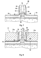
- a hole 74 is then formed ( figure 7 ) reaching the drain 26 by lithography and etching of the zones 36 and 34 of the electrically insulating assembly 28, and then growing through the hole 74, by selective epitaxy, a drain contact layer 76 made of silicon or SiGe x C y or a metal which is for example selected from cobalt, tungsten and titanium.
- the thickness of this layer is adjustable.
- the gate of the transistor is then formed on either side of the electrically insulating assembly 28 ( figure 7 ), while completing the drain contact.
- the grid is not necessarily metallic. It may be made of n + doped polycrystalline silicon (respectively p + ) for an n-channel transistor (respectively p), for example deposited by an LPCVD method.
- it may be made of a doped semiconductor material, for example silicon or germanium.
- a metal is deposited, which is for example chosen from cobalt, tungsten and titanium, on the structure obtained at figure 7 for example by chemical vapor deposition ("chemical vapor deposition").
- the metal thus deposited exceeds the upper level of the zone 36 made of silicon nitride.
- This metal is then planarized: this metal is polished, the zone 36 serving as a polishing stop layer.
- the planarized metallic layer 77 thus obtained, which extends in the hole 74 and on either side of the assembly 28.
- Zone 34 serves not only as an electrical insulation layer but also as a buffer layer.
- defects would be created if one formed silicon nitride directly on the drain 26, obtained by epitaxy and etching, and then buried silica, by thermal oxidation.
- the metal used to form the layer 77 Before depositing the metal used to form the layer 77, it is possible (but not essential) to fill the cavities 78 and 80 with metal ( figure 7 ) which exist under the spacers 42 and 44 because of the previous steps of the method.
- metal figure 7
- a chemical vapor deposition of cobalt, tungsten or titanium for example is used.
- the contacts of the transistor are then formed.
- the entire structure of the figure 8 is covered by an electrically insulating layer 86 ( figure 9 ) in silica glass doped with phosphorus or boron.
- Three openings are then formed which pass right through this layer 86 and open respectively to the two zones 77a and 77b of the metal layer 77 which correspond to the gate of the transistor and to the zone 77c of this layer 77, corresponding to the contact drain of the transistor.
- These three openings are filled with a metal, by chemical vapor deposition, to form two gate contacts 88 and 90 and a top drain contact 92.
- interconnecting metal layers 94, 96 and 98 are formed which respectively extend the contacts 88, 90 and 92.
- the source contact of the transistor is not shown. To obtain it, it is possible to according to the method of forming a metal layer on the underside of the substrate 18.
- p-type silicon was used for the substrate, but the invention naturally includes manufacturing processes that use an n-type silicon substrate. In this case, forming a p-type silicon + source, a type of n-channel silicon or SiGe x C y n-type and a p-type silicon drain. It is of course possible to use any other suitable semiconductor (n or p type) for forming the transistor.
- first gate metal for obtaining an n-channel transistor and a second gate metal, different from the first metal, for obtaining a p-channel transistor so as to obtain opposite threshold voltages.
- the figure 10 is a schematic and partial top view of an implementation diagram of an example of a vertical MOS transistor with a metal gate manufactured according to the invention.
- References 106, 108 and 110 respectively represent the drain contact, a gate contact and a source contact.
- Reference 112 represents the drain pre-contact and reference 114 represents a silicon pillar which corresponds to the set of referenced 28 including (42 and 44) on the figure 9 .
- the substrate on which this transistor is formed is not shown.
- the width of the transistor is four times greater than in the case of a conventional transistor because the gate 104 "surrounds" the silicon pillar 114 on all four sides. Guarding the grid-to-drain edge (that is, the space between the edge of the grid 104 (see figure 10 ) of that of the set 28 (see figure 9 ) is at most equal to the alignment tolerance given by the level-to-level lithography, ie the lithography that aligns the grid level with the drain level.
- the figure 11A is a schematic and partial view of a section of a transistor manufactured according to the invention. It illustrates the case where the "deposition" of the grid relative to the drain is zero.
- the invention makes it possible to admit a guard between the gate and the null drain because there will always remain a metal residue under the spacer, making it possible to produce a gate encasing the drain.
- the Figure 11B is a schematic and partial top view of the transistor of the figure 11A .
- This figure 11A corresponds to the AA cut of the Figure 11B .
- 11A and 11B 115 denotes the planarization and contact metal residues plus the gate metal.
- planarization and contact metal corresponds to reference 77b.
- the layers 82 correspond to the gate metal.
- the insulating layer 86 we also see the planarization and contact metal.
- CMOS technology with dual metal grids, this technology using an n + type extraction potential metal for the n-channel MOS transistors and a metal with an extraction potential of p + type for p-channel MOS transistors.
- the gate metal 77a, 77b and 77c, on the side where this metal is desired, is protected by a layer of silicon nitride 116.
- the silicon nitride layer referenced 116 thus serves as a stop layer for polishing the second metal, that is to say the metal referenced 77a, 77b and 77c.
Landscapes
- Engineering & Computer Science (AREA)
- Microelectronics & Electronic Packaging (AREA)
- Power Engineering (AREA)
- Physics & Mathematics (AREA)
- Ceramic Engineering (AREA)
- Condensed Matter Physics & Semiconductors (AREA)
- General Physics & Mathematics (AREA)
- Computer Hardware Design (AREA)
- Manufacturing & Machinery (AREA)
- Insulated Gate Type Field-Effect Transistor (AREA)
- Thin Film Transistor (AREA)
Claims (6)
- Verfahren zur Herstellung eines vertikalen MOS-Transistors, in welchem:- eine Struktur gebildet wird, die ein Halbleiter-Substrat (18), eine Source-Zone (27), eine Kanalzone (23) oberhalb der Source-Zone und einen Drain (26) oberhalb der Kanalzone aufweist,- oberhalb des Drain eine elektrisch isolierende Anordnung (28) gebildet wird, die elektrisch isolierende Zonen (42,44) beiderseits des Drain aufweist,- in der Struktur zwei Aussparungen (46,48) beiderseits der elektrisch isolierenden Anordnung gebildet werden, wobei die jeweiligen Flanken (46a,48a) dieser Aussparungen, die am nächsten zu der elektrisch isolierenden Anordnung gelegen sind, unterhalb letzterer beiderseits der Kanalzone angeordnet sind, um auf diese Weise Hohlräume (78, 80) zu bilden,- dünne elektrisch isolierende Schichten (70,72) mindestens an diesen Flanken der Aussparungen und andere dicke elektrisch isolierende Schichten (66,67) am Boden dieser Aussparungen gebildet werden, und- das Gate (77a, 77b) des Transistors beiderseits der elektrisch isolierenden Anordnung und bis in die Hohlräume gebildet wird,
in welchem zum Bilden der elektrisch isolierenden Anordnung- auf der Struktur eine erste Schicht (30), die elektrisch isolierend ist, und auf dieser ersten Schicht eine zweite Schicht (32), die ebenfalls elektrisch isolierend ist, gebildet werden,- diese erste und zweite Schicht geätzt werden, um so ein isolierendes Element (34,36) zu erzielen, das den Drain bedeckt,- oberhalb dieses isolierenden Elements eine dritte Schicht (38) gebildet wird, die ebenfalls elektrisch isolierend ist, und- diese dritte Schicht geätzt wird, um so die elektrisch isolierenden Zonen (42,44) zu bilden und die Bildung der elektrisch isolierenden Anordnung zu erreichen,
in welchem durch die elektrisch isolierende Anordnung hindurch ein Loch (74), das sich bis zu dem Drain erstreckt, gebildet wird und in diesem Loch eine Drainkontaktschicht (77c) gebildet wird,
und in welchem das Gate (77a, 77b) und diese Drainkontaktschicht (77c) gleichzeitig gebildet werden. - Verfahren nach Anspruch 1, in welchem die zweite Schicht (32) ferner geeignet ist, einer Metallschicht (77), die später gebildet wird und die für die Bildung des Gate (77a, 77b) des Transistors bestimmt ist, als Planarisationsstoppschicht zu dienen.
- Verfahren nach Anspruch 2, in welchem die zweite Schicht (32) aus Sliziumnitrid oder Siliziumcarbid ist.
- Verfahren nach Anspruch 3, in welchem die erste Schicht (30) ferner geeignet ist, als Pufferschicht zu dienen.
- Verfahren nach einem der Ansprüche 1 bis 4, in welchem die Source-Zone (27) gebildet wird durch Implantation von Ionen, die für eine Dotierung dieses Substrats geeignet sind, in das Substrat oder durch Epitaxie eines Halbleiters, der diese Dotierung hat, auf dieses Substrat.
- Verfahren nach einem der Ansprüche 1 bis 5, in welchem der Drain (26) mittels Epitaxie oder Ionenimplantation gebildet wird.
Applications Claiming Priority (3)
| Application Number | Priority Date | Filing Date | Title |
|---|---|---|---|
| FR0008016 | 2000-06-22 | ||
| FR0008016A FR2810792B1 (fr) | 2000-06-22 | 2000-06-22 | Transistor mos vertical a grille enterree et procede de fabrication de celui-ci |
| PCT/FR2001/001950 WO2001099197A1 (fr) | 2000-06-22 | 2001-06-21 | Transistor mos vertical a grille enterree et procede de fabrication de celui-ci |
Publications (2)
| Publication Number | Publication Date |
|---|---|
| EP1292991A1 EP1292991A1 (de) | 2003-03-19 |
| EP1292991B1 true EP1292991B1 (de) | 2011-05-11 |
Family
ID=8851568
Family Applications (1)
| Application Number | Title | Priority Date | Filing Date |
|---|---|---|---|
| EP01947563A Expired - Lifetime EP1292991B1 (de) | 2000-06-22 | 2001-06-21 | Verfahren zur Herstellung eines vertikalen MOS-Transistors mit vergrabenem Gate |
Country Status (5)
| Country | Link |
|---|---|
| US (2) | US20030132484A1 (de) |
| EP (1) | EP1292991B1 (de) |
| JP (1) | JP2003536276A (de) |
| FR (1) | FR2810792B1 (de) |
| WO (1) | WO2001099197A1 (de) |
Families Citing this family (14)
| Publication number | Priority date | Publication date | Assignee | Title |
|---|---|---|---|---|
| US8338887B2 (en) * | 2005-07-06 | 2012-12-25 | Infineon Technologies Ag | Buried gate transistor |
| JP4923543B2 (ja) * | 2005-11-30 | 2012-04-25 | トヨタ自動車株式会社 | 炭化珪素半導体装置及びその製造方法 |
| JP2009021439A (ja) * | 2007-07-12 | 2009-01-29 | Mitsubishi Electric Corp | 半導体装置及びその製造方法 |
| US9530866B1 (en) | 2016-04-13 | 2016-12-27 | Globalfoundries Inc. | Methods of forming vertical transistor devices with self-aligned top source/drain conductive contacts |
| US9799751B1 (en) | 2016-04-19 | 2017-10-24 | Globalfoundries Inc. | Methods of forming a gate structure on a vertical transistor device |
| US9640636B1 (en) | 2016-06-02 | 2017-05-02 | Globalfoundries Inc. | Methods of forming replacement gate structures and bottom and top source/drain regions on a vertical transistor device |
| US10347745B2 (en) | 2016-09-19 | 2019-07-09 | Globalfoundries Inc. | Methods of forming bottom and top source/drain regions on a vertical transistor device |
| US10170616B2 (en) | 2016-09-19 | 2019-01-01 | Globalfoundries Inc. | Methods of forming a vertical transistor device |
| US9882025B1 (en) | 2016-09-30 | 2018-01-30 | Globalfoundries Inc. | Methods of simultaneously forming bottom and top spacers on a vertical transistor device |
| US9966456B1 (en) | 2016-11-08 | 2018-05-08 | Globalfoundries Inc. | Methods of forming gate electrodes on a vertical transistor device |
| US9935018B1 (en) | 2017-02-17 | 2018-04-03 | Globalfoundries Inc. | Methods of forming vertical transistor devices with different effective gate lengths |
| US10229999B2 (en) | 2017-02-28 | 2019-03-12 | Globalfoundries Inc. | Methods of forming upper source/drain regions on a vertical transistor device |
| US10014370B1 (en) | 2017-04-19 | 2018-07-03 | Globalfoundries Inc. | Air gap adjacent a bottom source/drain region of vertical transistor device |
| US11075301B2 (en) | 2019-12-27 | 2021-07-27 | International Business Machines Corporation | Nanosheet with buried gate contact |
Citations (1)
| Publication number | Priority date | Publication date | Assignee | Title |
|---|---|---|---|---|
| EP0908938A2 (de) * | 1997-09-26 | 1999-04-14 | Siemens Aktiengesellschaft | Pufferschicht zum Verbessern der Schichtdickenkontrolle |
Family Cites Families (15)
| Publication number | Priority date | Publication date | Assignee | Title |
|---|---|---|---|---|
| US1995970A (en) * | 1931-04-04 | 1935-03-26 | Du Pont | Polymeric lactide resin |
| GB2103879B (en) * | 1981-08-19 | 1985-04-11 | Secr Defence | Method for producing a vertical channel transistor |
| NL8702563A (nl) * | 1987-10-28 | 1989-05-16 | Cca Biochem B V | Polymeer lactide, werkwijze voor het bereiden van een dergelijk polymeer lactide, alsmede een samenstelling, die een dergelijk polymeer lactide bevat. |
| JP2804539B2 (ja) * | 1989-09-28 | 1998-09-30 | 沖電気工業株式会社 | 半導体装置およびその製造方法 |
| US5087581A (en) * | 1990-10-31 | 1992-02-11 | Texas Instruments Incorporated | Method of forming vertical FET device with low gate to source overlap capacitance |
| JP3745392B2 (ja) * | 1994-05-26 | 2006-02-15 | 株式会社ルネサステクノロジ | 半導体装置 |
| US5757038A (en) * | 1995-11-06 | 1998-05-26 | International Business Machines Corporation | Self-aligned dual gate MOSFET with an ultranarrow channel |
| FR2749977B1 (fr) * | 1996-06-14 | 1998-10-09 | Commissariat Energie Atomique | Transistor mos a puits quantique et procedes de fabrication de celui-ci |
| DE19746901C2 (de) * | 1997-10-23 | 1999-08-12 | Siemens Ag | Verfahren zur Herstellung eines vertikalen MOS-Transistors |
| JPH11214684A (ja) * | 1998-01-26 | 1999-08-06 | Mitsubishi Electric Corp | 半導体装置およびその製造方法 |
| US6027975A (en) * | 1998-08-28 | 2000-02-22 | Lucent Technologies Inc. | Process for fabricating vertical transistors |
| US6107660A (en) * | 1999-05-19 | 2000-08-22 | Worldwide Semiconductor Manufacturing Corp. | Vertical thin film transistor |
| US6392271B1 (en) * | 1999-06-28 | 2002-05-21 | Intel Corporation | Structure and process flow for fabrication of dual gate floating body integrated MOS transistors |
| US6518622B1 (en) * | 2000-03-20 | 2003-02-11 | Agere Systems Inc. | Vertical replacement gate (VRG) MOSFET with a conductive layer adjacent a source/drain region and method of manufacture therefor |
| DE10020898B4 (de) * | 2000-04-20 | 2004-02-05 | Inventa-Fischer Gmbh | Verfahren zur Herstellung von Polymilchsäure und Vorrichtung hierzu |
-
2000
- 2000-06-22 FR FR0008016A patent/FR2810792B1/fr not_active Expired - Fee Related
-
2001
- 2001-06-21 WO PCT/FR2001/001950 patent/WO2001099197A1/fr active Application Filing
- 2001-06-21 US US10/311,216 patent/US20030132484A1/en not_active Abandoned
- 2001-06-21 JP JP2002503948A patent/JP2003536276A/ja active Pending
- 2001-06-21 EP EP01947563A patent/EP1292991B1/de not_active Expired - Lifetime
-
2007
- 2007-12-04 US US11/987,725 patent/US7666733B2/en not_active Expired - Fee Related
Patent Citations (1)
| Publication number | Priority date | Publication date | Assignee | Title |
|---|---|---|---|---|
| EP0908938A2 (de) * | 1997-09-26 | 1999-04-14 | Siemens Aktiengesellschaft | Pufferschicht zum Verbessern der Schichtdickenkontrolle |
Also Published As
| Publication number | Publication date |
|---|---|
| EP1292991A1 (de) | 2003-03-19 |
| FR2810792B1 (fr) | 2003-07-04 |
| WO2001099197A1 (fr) | 2001-12-27 |
| FR2810792A1 (fr) | 2001-12-28 |
| JP2003536276A (ja) | 2003-12-02 |
| US20080096354A1 (en) | 2008-04-24 |
| US7666733B2 (en) | 2010-02-23 |
| US20030132484A1 (en) | 2003-07-17 |
Similar Documents
| Publication | Publication Date | Title |
|---|---|---|
| EP1266409B1 (de) | Mos-transistor mit metallischen source- und draingebieten und dessen herstellungsverfahren | |
| EP1292991B1 (de) | Verfahren zur Herstellung eines vertikalen MOS-Transistors mit vergrabenem Gate | |
| EP1589572B1 (de) | Verfahren zur Herstellung einer integrierten Schaltung mit einem Isolationsgraben | |
| EP2323160A1 (de) | Verfahren zur Herstellung von Feldeffekttransistoren mit einer Gegenelektrode und Halbleitervorrichtung | |
| FR2593640A1 (fr) | Dispositif semi-conducteur monolithique integre comportant des transistors a jonction bipolaire, des transistors cmos et dmos, des diodes a faible fuite et procede pour sa fabrication | |
| US10276685B2 (en) | Heterojunction tunnel field effect transistor fabrication using limited lithography steps | |
| FR3047838A1 (fr) | Transistor bipolaire et son procede de fabrication | |
| US20180286946A1 (en) | Novel sti process for sdb devices | |
| FR2985089A1 (fr) | Transistor et procede de fabrication d'un transistor | |
| FR2795554A1 (fr) | Procede de gravure laterale par trous pour fabriquer des dis positifs semi-conducteurs | |
| EP1406307A1 (de) | Integrierte Schaltung mit einer hochleitenden begrabenen Schicht | |
| FR2990295A1 (fr) | Procede de formation de contacts de grille, de source et de drain sur un transistor mos | |
| EP2120258B1 (de) | Herstellungsverfahren eines Transistors mit Metallquelle und -abfluss | |
| FR3003691A1 (fr) | Finfet avec grille arriere | |
| EP3442027B1 (de) | Verfahren zur bildung von dotierten erweiterungsbereichen in einer struktur mit übereinander angeordneten nanodrähten | |
| FR2860919A1 (fr) | Structures et procedes de fabrication de regions semiconductrices sur isolant | |
| FR2806833A1 (fr) | Procede de fabrication d'un transistor mos a deux grilles, dont l'une est enterree, et transistor correspondant | |
| FR3067516A1 (fr) | Realisation de regions semiconductrices dans une puce electronique | |
| EP0522938B1 (de) | Verfahren zum Herstellen eines vertikalen Feldeffekt-Transistors und durch dieses Verfahren hergestellter Transistor | |
| FR2976401A1 (fr) | Composant electronique comportant un ensemble de transistors mosfet et procede de fabrication | |
| EP0675544A1 (de) | Verfahren zur Herstellung eines Feldeffekttransistors mit isoliertem Gatter und kurzem Kanal, und entsprechender Transistor | |
| EP1407486B1 (de) | Herstellungsverfahren für einen transistor auf einem soi-substrat | |
| WO2018007711A1 (fr) | Dispositif cascode integre monolithiquement | |
| FR3035265A1 (fr) | Procede de fabrication de transistors soi pour une densite d'integration accrue | |
| WO2007017613A1 (fr) | Procede de fabrication d'un transistor a nanodoigts semiconducteurs paralleles |
Legal Events
| Date | Code | Title | Description |
|---|---|---|---|
| PUAI | Public reference made under article 153(3) epc to a published international application that has entered the european phase |
Free format text: ORIGINAL CODE: 0009012 |
|
| 17P | Request for examination filed |
Effective date: 20021203 |
|
| AK | Designated contracting states |
Kind code of ref document: A1 Designated state(s): AT BE CH CY DE DK ES FI FR GB GR IE IT LI LU MC NL PT SE TR |
|
| RBV | Designated contracting states (corrected) |
Designated state(s): AT BE CH CY DE FR GB IT LI |
|
| RAP1 | Party data changed (applicant data changed or rights of an application transferred) |
Owner name: COMMISSARIAT A L'ENERGIE ATOMIQUE |
|
| RAP1 | Party data changed (applicant data changed or rights of an application transferred) |
Owner name: COMMISSARIAT A L'ENERGIE ATOMIQUE ET AUX ENERGIES |
|
| 17Q | First examination report despatched |
Effective date: 20100419 |
|
| RIC1 | Information provided on ipc code assigned before grant |
Ipc: H01L 29/45 20060101ALN20101018BHEP Ipc: H01L 29/49 20060101ALN20101018BHEP Ipc: H01L 29/06 20060101ALI20101018BHEP Ipc: H01L 29/78 20060101ALI20101018BHEP Ipc: H01L 21/336 20060101AFI20101018BHEP |
|
| RTI1 | Title (correction) |
Free format text: METHOD OF MAKING A VERTICAL MOS TRANSISTOR HAVING A BURIED GATE |
|
| GRAP | Despatch of communication of intention to grant a patent |
Free format text: ORIGINAL CODE: EPIDOSNIGR1 |
|
| RBV | Designated contracting states (corrected) |
Designated state(s): DE FR GB IT |
|
| GRAS | Grant fee paid |
Free format text: ORIGINAL CODE: EPIDOSNIGR3 |
|
| GRAA | (expected) grant |
Free format text: ORIGINAL CODE: 0009210 |
|
| AK | Designated contracting states |
Kind code of ref document: B1 Designated state(s): DE FR GB IT |
|
| REG | Reference to a national code |
Ref country code: GB Ref legal event code: FG4D Free format text: NOT ENGLISH |
|
| REG | Reference to a national code |
Ref country code: DE Ref legal event code: R096 Ref document number: 60144608 Country of ref document: DE Effective date: 20110622 |
|
| PLBE | No opposition filed within time limit |
Free format text: ORIGINAL CODE: 0009261 |
|
| STAA | Information on the status of an ep patent application or granted ep patent |
Free format text: STATUS: NO OPPOSITION FILED WITHIN TIME LIMIT |
|
| 26N | No opposition filed |
Effective date: 20120214 |
|
| REG | Reference to a national code |
Ref country code: DE Ref legal event code: R097 Ref document number: 60144608 Country of ref document: DE Effective date: 20120214 |
|
| PG25 | Lapsed in a contracting state [announced via postgrant information from national office to epo] |
Ref country code: IT Free format text: LAPSE BECAUSE OF NON-PAYMENT OF DUE FEES Effective date: 20120621 |
|
| PGFP | Annual fee paid to national office [announced via postgrant information from national office to epo] |
Ref country code: GB Payment date: 20130620 Year of fee payment: 13 |
|
| PGFP | Annual fee paid to national office [announced via postgrant information from national office to epo] |
Ref country code: DE Payment date: 20140610 Year of fee payment: 14 |
|
| GBPC | Gb: european patent ceased through non-payment of renewal fee |
Effective date: 20140621 |
|
| PG25 | Lapsed in a contracting state [announced via postgrant information from national office to epo] |
Ref country code: GB Free format text: LAPSE BECAUSE OF NON-PAYMENT OF DUE FEES Effective date: 20140621 |
|
| REG | Reference to a national code |
Ref country code: DE Ref legal event code: R119 Ref document number: 60144608 Country of ref document: DE |
|
| PG25 | Lapsed in a contracting state [announced via postgrant information from national office to epo] |
Ref country code: DE Free format text: LAPSE BECAUSE OF NON-PAYMENT OF DUE FEES Effective date: 20160101 |
|
| REG | Reference to a national code |
Ref country code: FR Ref legal event code: PLFP Year of fee payment: 16 |
|
| PGFP | Annual fee paid to national office [announced via postgrant information from national office to epo] |
Ref country code: FR Payment date: 20160708 Year of fee payment: 16 |
|
| REG | Reference to a national code |
Ref country code: FR Ref legal event code: ST Effective date: 20180228 |
|
| PG25 | Lapsed in a contracting state [announced via postgrant information from national office to epo] |
Ref country code: FR Free format text: LAPSE BECAUSE OF NON-PAYMENT OF DUE FEES Effective date: 20170630 |