EP1291922A1 - Kontaktstruktur auf einem in einem Halbleitersubstrat gebildeten tiefen Gebiet - Google Patents
Kontaktstruktur auf einem in einem Halbleitersubstrat gebildeten tiefen Gebiet Download PDFInfo
- Publication number
- EP1291922A1 EP1291922A1 EP02354133A EP02354133A EP1291922A1 EP 1291922 A1 EP1291922 A1 EP 1291922A1 EP 02354133 A EP02354133 A EP 02354133A EP 02354133 A EP02354133 A EP 02354133A EP 1291922 A1 EP1291922 A1 EP 1291922A1
- Authority
- EP
- European Patent Office
- Prior art keywords
- region
- type
- conductivity
- deep
- trench
- Prior art date
- Legal status (The legal status is an assumption and is not a legal conclusion. Google has not performed a legal analysis and makes no representation as to the accuracy of the status listed.)
- Pending
Links
- 239000000758 substrate Substances 0.000 title claims description 45
- 239000004065 semiconductor Substances 0.000 title claims description 4
- XUIMIQQOPSSXEZ-UHFFFAOYSA-N Silicon Chemical compound [Si] XUIMIQQOPSSXEZ-UHFFFAOYSA-N 0.000 claims abstract description 54
- 229910052710 silicon Inorganic materials 0.000 claims abstract description 52
- 239000010703 silicon Substances 0.000 claims abstract description 52
- 239000002019 doping agent Substances 0.000 claims description 17
- 238000009792 diffusion process Methods 0.000 claims description 10
- 238000000137 annealing Methods 0.000 claims description 7
- 238000000034 method Methods 0.000 claims description 7
- 238000002513 implantation Methods 0.000 claims description 5
- 239000003989 dielectric material Substances 0.000 claims description 4
- 238000005530 etching Methods 0.000 claims description 2
- 229910021421 monocrystalline silicon Inorganic materials 0.000 claims description 2
- 230000015572 biosynthetic process Effects 0.000 abstract 1
- 239000010410 layer Substances 0.000 description 20
- 238000004519 manufacturing process Methods 0.000 description 8
- 229910052698 phosphorus Inorganic materials 0.000 description 7
- 239000011574 phosphorus Substances 0.000 description 7
- OAICVXFJPJFONN-UHFFFAOYSA-N Phosphorus Chemical compound [P] OAICVXFJPJFONN-UHFFFAOYSA-N 0.000 description 6
- 230000007704 transition Effects 0.000 description 6
- 150000002500 ions Chemical class 0.000 description 5
- 230000008569 process Effects 0.000 description 5
- 229910052785 arsenic Inorganic materials 0.000 description 4
- -1 boron ions Chemical class 0.000 description 4
- 230000003071 parasitic effect Effects 0.000 description 4
- 238000009413 insulation Methods 0.000 description 3
- 230000010354 integration Effects 0.000 description 3
- 244000045947 parasite Species 0.000 description 3
- 239000011347 resin Substances 0.000 description 3
- 229920005989 resin Polymers 0.000 description 3
- RQNWIZPPADIBDY-UHFFFAOYSA-N arsenic atom Chemical compound [As] RQNWIZPPADIBDY-UHFFFAOYSA-N 0.000 description 2
- 229910052796 boron Inorganic materials 0.000 description 2
- 238000005516 engineering process Methods 0.000 description 2
- 239000007943 implant Substances 0.000 description 2
- 238000005036 potential barrier Methods 0.000 description 2
- 230000009467 reduction Effects 0.000 description 2
- ZOXJGFHDIHLPTG-UHFFFAOYSA-N Boron Chemical compound [B] ZOXJGFHDIHLPTG-UHFFFAOYSA-N 0.000 description 1
- 229910052581 Si3N4 Inorganic materials 0.000 description 1
- 230000004913 activation Effects 0.000 description 1
- 230000008859 change Effects 0.000 description 1
- 230000003247 decreasing effect Effects 0.000 description 1
- 238000000407 epitaxy Methods 0.000 description 1
- 238000010438 heat treatment Methods 0.000 description 1
- 238000005468 ion implantation Methods 0.000 description 1
- 238000002955 isolation Methods 0.000 description 1
- 230000004048 modification Effects 0.000 description 1
- 238000012986 modification Methods 0.000 description 1
- 238000000206 photolithography Methods 0.000 description 1
- 238000005498 polishing Methods 0.000 description 1
- 229910021420 polycrystalline silicon Inorganic materials 0.000 description 1
- 239000011241 protective layer Substances 0.000 description 1
- 238000011084 recovery Methods 0.000 description 1
- HQVNEWCFYHHQES-UHFFFAOYSA-N silicon nitride Chemical compound N12[Si]34N5[Si]62N3[Si]51N64 HQVNEWCFYHHQES-UHFFFAOYSA-N 0.000 description 1
- 239000000126 substance Substances 0.000 description 1
- 230000001960 triggered effect Effects 0.000 description 1
Images


Classifications
-
- H—ELECTRICITY
- H01—ELECTRIC ELEMENTS
- H01L—SEMICONDUCTOR DEVICES NOT COVERED BY CLASS H10
- H01L29/00—Semiconductor devices specially adapted for rectifying, amplifying, oscillating or switching and having potential barriers; Capacitors or resistors having potential barriers, e.g. a PN-junction depletion layer or carrier concentration layer; Details of semiconductor bodies or of electrodes thereof ; Multistep manufacturing processes therefor
- H01L29/02—Semiconductor bodies ; Multistep manufacturing processes therefor
- H01L29/06—Semiconductor bodies ; Multistep manufacturing processes therefor characterised by their shape; characterised by the shapes, relative sizes, or dispositions of the semiconductor regions ; characterised by the concentration or distribution of impurities within semiconductor regions
- H01L29/08—Semiconductor bodies ; Multistep manufacturing processes therefor characterised by their shape; characterised by the shapes, relative sizes, or dispositions of the semiconductor regions ; characterised by the concentration or distribution of impurities within semiconductor regions with semiconductor regions connected to an electrode carrying current to be rectified, amplified or switched and such electrode being part of a semiconductor device which comprises three or more electrodes
- H01L29/0821—Collector regions of bipolar transistors
Definitions
- the present invention relates to the field of circuits integrated and more particularly the creation of a structure of contact with a deep and doped region in a substrate of silicon.
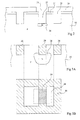
- Certain electronic components constituting the integrated circuits are made vertically. This is the case, for example, vertical bipolar transistors.
- the transmitter and base of the vertical bipolar transistor lie on the surface of the silicon wafer.
- the collector of the bipolar transistor is deep in the substrate. We must then carry out the connection between the deep collector and the integrated circuit surface interconnections.
- ions doping the substrate 1 are boron ions with a concentration of 1x10 15 at / cm 3 .
- the region 2 doping ions are arsenic ions with a concentration of 5 ⁇ 10 19 at / cm 3 .
- the ions doping the epitaxial layer 3 are phosphorus ions with a concentration of 5 ⁇ 10 15 at / cm 3 .
- This bipolar transistor has a silicon well 5, a intrinsic collector 6, a base 8 and a transmitter 9.
- the silicon well 5 is a region of silicon, of the same type of conductivity N as region 2, which connects the region buried 2 on the surface of the slice.
- the intrinsic collector 6 is a silicon region of the same type of conductivity as the buried region 2 and in electrical contact with it thanks to an implanted transition region 7 of the same type of conductivity as regions 6 and 2.
- the base 8 of the transistor bipolar is a silicon region of the conductivity type P located on the surface of the substrate. Base 8 is made at inside the epitaxial layer 3 and is located above the intrinsic collector 6.
- the emitter 9 is a region of type N conductivity, heavily doped and strictly included in the base 8. In order to isolate the various elements laterally constitutive of the bipolar transistor we use trenches 4 filled with oxide. We thus completely surround base 8 with the trench 4 in order to isolate it laterally from the silicon well 5.
- FIG. 1B top view of FIG. 1A, represents the trench 4 entirely surrounding the base 8 and the collector well 5.
- the other regions of FIG. 1A are not not shown, for reasons of clarity, in this figure 1B.
- Contacts on the transmitter, base and collector are not shown in Figure 1B.
- the capacity between the collector and the substrate of the bipolar transistor also needs to be optimized so improve the performance of the bipolar transistor.
- This capacity is proportional to the area of the junction between regions 2 and substrate 1. It is necessary to improve the bipolar transistor performance reduce the size of the region 2 without increasing any internal resistance of the device.
- An object of the present invention is to allow the decrease in internal resistance of a device using a deep doped region and decreased capacity parasite of said deep region, i.e. reduction dimensions of said deep region.
- Another object of the present invention is increase the performance of bipolar transistors vertical.
- Another object of the present invention is to significantly reduce the costs of manufacturing the devices requiring contact to a deep layer of silicon dope.
- the present invention provides a contact structure with a deep region of a first type of conductivity formed in a semiconductor substrate, having a trench adjacent to the deep region; an intermediate region of the first type of conductivity located below the trench and in electrical contact with the deep region; and a doped silicon well of the first type conductivity in electrical contact with the region intermediate and disjoint from the deep region.
- the first type of conductivity is N; the substrate is monocrystalline silicon whose type of conductivity is P; the doping of the deep region is greater than 5 ⁇ 10 18 at / cm 3 ; the doping of the intermediate region is greater than 1x10 19 at / cm 3 ; and the doping of the doped silicon well is greater than 1x10 19 at / cm 3 .
- the intermediate region partially covers the region deep and the doped silicon well.
- the deep region is bounded laterally, at least in its upper part, by a trench.
- the deep region, the intermediate region and the doped well constitute the contact of the collector of a transistor bipolar.
- the deep region forms the deep base of a transistor bipolar and the intermediate region and the doped well constitute the contact on the deep base of the transistor bipolar.
- the deep region is arranged between a box of a second type of conductivity and the substrate of a second type of conductivity to isolate the box from the substrate.
- a trench filled with at least one dielectric material delimits the implantation of the dopant of the first type of conductivity in the deep region.
- the deep region and the filled trench isolate the substrate initial substrate of a second type of conductivity of a MOS transistor.
- FIG. 2 represents an initial step in the production of a contact structure on a deep region according to the present invention.
- a protective layer 21, for example 100 nm thick silicon nitride, is deposited on a P-type silicon substrate 10.
- the layer 21 is etched and trenches are created in the upper part of the silicon substrate 10, for example according to the pattern illustrated in the top view of FIG. 1B. Three trench cuts are shown.
- a resin mask 24 creates an opening 25 in line with the central trench 27.
- Arsenic is implanted at a dose of less than 5 ⁇ 10 16 at / cm 2 and with an energy of less than 100 keV through this opening.
- the arsenic ions are then stopped by the resin 24 or the layer 21 so that only the bottom of the central trench 27 is implanted in a silicon region 26.
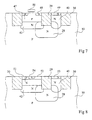
- Figures 3A and 3B show a next step of the realization of the contact structure on a region deep according to the present invention.
- Figure 3A shows part of the silicon substrate seen in section;
- Figure 3B represents a part of the silicon substrate seen from above.
- a chemical mechanical polishing step and annealing complete the process of creating insulating trenches.
- Below the central trench a intermediate region of type 28 silicon is obtained by diffusion of dopants, implanted in region 26, during said annealing.
- Figure 3B represents two entirely surrounded silicon regions of a trench 29, 30.
- FIG. 4 illustrates a next step in the method of manufacturing the contact structure on a deep region.
- High-dose phosphorus is implanted to form a doped silicon well 40 located between the central trench 29 and the right trench.
- phosphorus is implanted with a dose of between 2x10 15 and 2x10 16 at / cm 2 with an energy of 400 keV.
- Annealing for example of 950 ° C. for twenty minutes, allows the diffusion of this well 40 so that it partially covers the intermediate region 28 in a silicon region 41.
- the silicon well 40 being bounded by trenches , does not extend laterally even in the event of significant thermal diffusion of the dopants.
- High energy phosphorus is then implanted in a deep silicon region 42 located between the central trench 29 and the left trench.
- the trenches mask and laterally limit this settlement.
- phosphorus is implanted with a dose of between 5 ⁇ 10 14 and 2 ⁇ 10 16 16 at / cm 3 with an energy greater than 300 keV. Rapid annealing, for example of 1000 ° C. for 10 s, allows the electrical activation of the implanted phosphorus without causing significant diffusion.
- the deep region 42, of type N covers part of the intermediate region 28 of type N, previously diffused, in a region of silicon 43.
- the region 42 delimits a box of silicon 44 of type P whose borders are the deep region 42, the trenches and the surface of the substrate.
- the well 44 has the type and the level of doping of the initial substrate. It is then, in the case of the present example, entirely isolated from the P-type substrate 10 as well. In fact, the box 44 is isolated vertically by junctions and laterally by the trenches.
- regions 42, 28, 40 of the FIG. 4 are similar respectively to those of regions 7, 2, 5 of Figure 1A.
- the deep region 42 is like the region 7, a transition region for the current. She also has a role of vertical insulation which requires an increase in sound doping.
- the intermediate region 28 has a role similar to that of the buried layer 2: it conducts the current of the region deep 42 towards the doped silicon well 40. However the dimensions of this intermediate region are greatly reduced by compared to those of the buried layer 2. Capacities parasites and the resistances associated with this layer will also very small.
- Figure 4 allows better compromise for the integration of devices requiring buried layer. It is not limited when the dimensions devices decrease. It is all the more effective as the dimensions are small, less than 0.5 ⁇ m and preferably less than 0.1 ⁇ m.
- the process is economical because no epitaxy step, expensive in an industrial environment, has not been used.
- the doping profiles obtained by this process are reproducible because they are obtained from implantations ionic and limited thermal annealing. The yield of manufacturing of integrated circuits is improved.
- FIG. 5 represents the doping profile along the axis vertical AA ′ in FIG. 4.
- This axis AA ′ crosses the box 44 and the deep layer 42 perpendicular to the surface of the silicon.
- the abscissa axis represents the depth (d) at from the surface of substrate 10
- the ordinate axis represents the concentration (c) of doping atoms on a scale logarithmic.
- This doping profile demonstrates the isolation by vertically junctions of the silicon box 44 of P type with respect to P type substrate 10. To obtain this insulation it is necessary to reverse polarize the two N / P junctions created between regions 42 and 44 on the one hand and between the region 42 and the substrate 10 on the other hand. Positive tension must be applied to deep region 42, using the region intermediate 28 and well 40.
- Figure 6 shows the concentration c as a function of the depth d along the vertical axis BB 'of FIG. 4.
- This axis BB ' crosses the doped silicon well 40, the region 41 and region 28.
- This doping profile demonstrates continuity between regions 40 and 28 and in particular the superimposition of the concentrations of the doping atoms of the regions 40 and 28 in the region 41.
- This over-concentration of the region 41 associated with the shallow depth of the doped well 40 allows obtain minimum resistance for current flow successively crossing regions 40 and 28 in the direction of axis BB '.
- Figure 7 shows the structure of a transistor Lateral MOS according to the present invention, the box of which is fully insulated. From technological operations performed in Figure 4, an ionic implantation of boron is made in the silicon box 44 now designated by reference 47.
- This layout allows the adjustment of the doping level of the silicon substrate 47 of the future transistor MOS.
- Conventionally we grow a gate oxide, we deposit and etch polycrystalline silicon 50 which forms the gate of the MOS transistor.
- the substrate 47 of this MOS transistor is fully isolated from the initial substrate 10 as long as a positive potential difference exists between deep region 42 and silicon regions adjacent opposite doping.
- This configuration known as name of triple box was obtained without heat treatment important - which is incompatible with the processes of submicronic manufacturing - and without growth of a layer of epitaxial silicon.
- the level of doping of region 42 allows to adjust the voltage withstand of the substrate 47 of the MOS transistor with respect to the initial substrate 10 and to reduce the gain of the parasitic bipolar transistor formed by the substrate 47 of the MOS transistor, deep region 42, and the initial substrate 10.
- the parasitic thyristor generated by sources and drains 48 of the MOS transistor, the insulated box 47, the deep region 42 and the substrate 10 is also an important parameter for optimizing this structure. In particular this thyristor parasite cannot be triggered if the potential of the area deep 42 is well controlled.
- the resistance to access to the deep region 42 across the region intermediate 28 and the doped silicon well 40 is weak.
- the present invention allows easy control of all physical parameters of regions 49, 40, 28, 42, 47 so optimize this triple box structure.
- the compactness of the structure obtained allows easy integration into high integration density digital circuits using MOS transistors. This compactness also makes it possible to reduce all internal parasitic resistances and thus avoid the nuisance triggering of parasitic thyristors.
- Figure 8 shows the structure of a transistor bipolar according to the present invention. From operations shown in Figure 4, an implementation is carried out phosphorus in region 44. This location compensates the initial P-type doping level of this region and allows to locally obtain a region 51 whose doping is of type N. By current operations in bipolar technology we realize then the base 52 of the bipolar transistor, the contact point 53 of the collector and the emitter region 54. The present invention allows to obtain a low resistance between the collector intrinsic 51 of the bipolar transistor and the collector socket 53. The surface between zones 42, 28, 40 on the one hand and on the other apart the substrate 10 is minimized and circumscribed inside of the perimeter defined by the trenches surrounding the transistor bipolar. The capacity of the collector of the bipolar transistor is low. The two features above allow significantly increase the dynamic performance of the component, in particular the maximum operating frequency (Furax) as well as the transition frequency (Ft).
- Furax maximum operating frequency
- Ft transition frequency
- the present invention is capable of various variations and modifications that will appear to humans art.
- any type of substrate can be used. departure as long as there is a weakly layer on its surface doped.
- the epitaxial substrates used in MOS technology are suitable for the present invention. These silicon substrates, very strongly doped in volume, have a layer of epitaxial silicon on their front face 10 to 20 ⁇ m thick and lightly doped.
- any device operating vertically, the current to be collected in volume, can advantageously be made from the present invention.
Landscapes
- Engineering & Computer Science (AREA)
- Microelectronics & Electronic Packaging (AREA)
- Power Engineering (AREA)
- Physics & Mathematics (AREA)
- Ceramic Engineering (AREA)
- Condensed Matter Physics & Semiconductors (AREA)
- General Physics & Mathematics (AREA)
- Computer Hardware Design (AREA)
- Bipolar Transistors (AREA)
Applications Claiming Priority (2)
| Application Number | Priority Date | Filing Date | Title |
|---|---|---|---|
| FR0111556 | 2001-09-06 | ||
| FR0111556A FR2829288A1 (fr) | 2001-09-06 | 2001-09-06 | Structure de contact sur une region profonde formee dans un substrat semiconducteur |
Publications (1)
| Publication Number | Publication Date |
|---|---|
| EP1291922A1 true EP1291922A1 (de) | 2003-03-12 |
Family
ID=8867040
Family Applications (1)
| Application Number | Title | Priority Date | Filing Date |
|---|---|---|---|
| EP02354133A Pending EP1291922A1 (de) | 2001-09-06 | 2002-09-04 | Kontaktstruktur auf einem in einem Halbleitersubstrat gebildeten tiefen Gebiet |
Country Status (3)
| Country | Link |
|---|---|
| US (1) | US6847094B2 (de) |
| EP (1) | EP1291922A1 (de) |
| FR (1) | FR2829288A1 (de) |
Cited By (1)
| Publication number | Priority date | Publication date | Assignee | Title |
|---|---|---|---|---|
| EP1702349A2 (de) * | 2003-12-31 | 2006-09-20 | Freescale Semiconductor Inc. | Verfahren zur herstellung einer halbleiterkomponente und dadurch gebildete halbleiterkomponente |
Families Citing this family (3)
| Publication number | Priority date | Publication date | Assignee | Title |
|---|---|---|---|---|
| US6812486B1 (en) * | 2003-02-20 | 2004-11-02 | National Semiconductor Corporation | Conductive structure and method of forming the structure |
| US6815714B1 (en) * | 2003-02-20 | 2004-11-09 | National Semiconductor Corporation | Conductive structure in a semiconductor material |
| US7994536B2 (en) * | 2008-02-19 | 2011-08-09 | Qimonda Ag | Integrated circuit including U-shaped access device |
Citations (3)
| Publication number | Priority date | Publication date | Assignee | Title |
|---|---|---|---|---|
| EP0004292A2 (de) * | 1978-03-27 | 1979-10-03 | International Business Machines Corporation | Verfahren zum Herstellen eines MESA bipolaren Transistors mit selbstausgerichteten Emitter- und Basisbereichen |
| US6184102B1 (en) * | 1996-12-10 | 2001-02-06 | Sgs-Thomson Microelectronics S.A. | Method for manufacturing a well isolation bipolar transistor |
| US6265275B1 (en) * | 1998-06-05 | 2001-07-24 | Stmicroelectronics S.A. | Method of selectively doping the intrinsic collector of a vertical bipolar transistor with epitaxial base |
Family Cites Families (13)
| Publication number | Priority date | Publication date | Assignee | Title |
|---|---|---|---|---|
| JPS5226182A (en) * | 1975-08-25 | 1977-02-26 | Hitachi Ltd | Manufacturing method of semi-conductor unit |
| US4392149A (en) * | 1980-03-03 | 1983-07-05 | International Business Machines Corporation | Bipolar transistor |
| JPS61164262A (ja) * | 1985-01-17 | 1986-07-24 | Toshiba Corp | 半導体装置 |
| US4851362A (en) * | 1987-08-25 | 1989-07-25 | Oki Electric Industry Co., Ltd. | Method for manufacturing a semiconductor device |
| US5006476A (en) * | 1988-09-07 | 1991-04-09 | North American Philips Corp., Signetics Division | Transistor manufacturing process using three-step base doping |
| US5124775A (en) * | 1990-07-23 | 1992-06-23 | National Semiconductor Corporation | Semiconductor device with oxide sidewall |
| JPH04105325A (ja) * | 1990-08-24 | 1992-04-07 | Hitachi Ltd | 半導体集積回路装置 |
| JPH04209540A (ja) * | 1990-12-04 | 1992-07-30 | Takehide Shirato | バイポーラトランジスタ |
| US5187109A (en) * | 1991-07-19 | 1993-02-16 | International Business Machines Corporation | Lateral bipolar transistor and method of making the same |
| JPH07106412A (ja) * | 1993-10-07 | 1995-04-21 | Toshiba Corp | 半導体装置およびその製造方法 |
| JP2679639B2 (ja) * | 1994-09-12 | 1997-11-19 | 日本電気株式会社 | 半導体装置及びその製造方法 |
| US5869881A (en) * | 1994-12-20 | 1999-02-09 | Electronics And Telecommunications Research Institute | Pillar bipolar transistor |
| EP0818829A1 (de) * | 1996-07-12 | 1998-01-14 | Hitachi, Ltd. | Bipolartransistor und dessen Herstellungsverfahren |
-
2001
- 2001-09-06 FR FR0111556A patent/FR2829288A1/fr active Pending
-
2002
- 2002-09-04 EP EP02354133A patent/EP1291922A1/de active Pending
- 2002-09-06 US US10/236,082 patent/US6847094B2/en not_active Expired - Lifetime
Patent Citations (3)
| Publication number | Priority date | Publication date | Assignee | Title |
|---|---|---|---|---|
| EP0004292A2 (de) * | 1978-03-27 | 1979-10-03 | International Business Machines Corporation | Verfahren zum Herstellen eines MESA bipolaren Transistors mit selbstausgerichteten Emitter- und Basisbereichen |
| US6184102B1 (en) * | 1996-12-10 | 2001-02-06 | Sgs-Thomson Microelectronics S.A. | Method for manufacturing a well isolation bipolar transistor |
| US6265275B1 (en) * | 1998-06-05 | 2001-07-24 | Stmicroelectronics S.A. | Method of selectively doping the intrinsic collector of a vertical bipolar transistor with epitaxial base |
Cited By (2)
| Publication number | Priority date | Publication date | Assignee | Title |
|---|---|---|---|---|
| EP1702349A2 (de) * | 2003-12-31 | 2006-09-20 | Freescale Semiconductor Inc. | Verfahren zur herstellung einer halbleiterkomponente und dadurch gebildete halbleiterkomponente |
| EP1702349A4 (de) * | 2003-12-31 | 2010-09-15 | Freescale Semiconductor Inc | Verfahren zur herstellung einer halbleiterkomponente und dadurch gebildete halbleiterkomponente |
Also Published As
| Publication number | Publication date |
|---|---|
| US20030042574A1 (en) | 2003-03-06 |
| US6847094B2 (en) | 2005-01-25 |
| FR2829288A1 (fr) | 2003-03-07 |
Similar Documents
| Publication | Publication Date | Title |
|---|---|---|
| EP0057126B1 (de) | Verfahren zur Herstellung einer Transistorstruktur | |
| FR2652448A1 (fr) | Procede de fabrication d'un circuit integre mis haute tension. | |
| EP0820637A1 (de) | VERFAHREN ZUR EINFÜHRUNG EINER IN SiC DOTIERENDER VERUNREINIGUNG; DADURCH HERGESTELLTES HALBLEITERBAUELEMENT UND GEBRAUCH EINER HOCHDOTIERTEN AMORPHEN SCHICHT ALS DOTIERSTOFFQUELLE ZUR DIFFUNDIERUNG IN SiC | |
| EP0462882A1 (de) | Dünnfilm-Feldeffekttransistor mit vergrabenem Gate und Verfahren zur Herstellung | |
| FR2530867A1 (fr) | Dispositifs mos a barriere de schottky et leur procede de fabrication | |
| US20050215024A1 (en) | Methods for forming super-steep diffusion region profiles in MOS devices and resulting semiconductor topographies | |
| FR2649831A1 (fr) | Dispositif soi-mos presentant une structure de paroi laterale conductrice et procede pour sa fabrication | |
| EP2325893A2 (de) | Bidirektionale Schutzdiode für niedrige Spannungen | |
| EP1214737B1 (de) | Verfahren zur herstellung einer schottky varicap diode | |
| US8476143B2 (en) | Deep contacts of integrated electronic devices based on regions implanted through trenches | |
| US5147809A (en) | Method of producing a bipolar transistor with a laterally graded emitter (LGE) employing a refill method of polycrystalline silicon | |
| EP1146561A1 (de) | Herstellungverfahren für einen Bipolartransistor | |
| EP1291922A1 (de) | Kontaktstruktur auf einem in einem Halbleitersubstrat gebildeten tiefen Gebiet | |
| FR2482368A1 (fr) | Operateur logique a injection par le substrat et son procede de fabrication | |
| FR2742583A1 (fr) | Transistor a effet de champ a grille isolee et a canal diffuse | |
| KR20000062635A (ko) | 상보형 금속 산화 반도체 장치용 2중 게이트 구조 제조 방법 | |
| JP3361842B2 (ja) | 半導体素子、システム及び方法 | |
| US6599817B1 (en) | Semiconductor constructions, and methods of forming semiconductor constructions | |
| US7479438B2 (en) | Method to improve performance of a bipolar device using an amorphizing implant | |
| EP0037764B1 (de) | Unipolar funktionierende Halbleiterbauelementenstruktur mit Schutzring | |
| TW201924060A (zh) | 具有減小的橫向電場之電晶體元件 | |
| EP1146554A1 (de) | Verfahren zur Herstellung vergrabener Schichten | |
| EP0948038B1 (de) | Herstellungsverfahren für eine Avalanche-Diode mit steuerbarem Schwellwert | |
| FR2784503A1 (fr) | Composant elementaire micro-electronique conjuguant l'effet bipolaire et l'effet mos, procede de fabrication d'un tel composant | |
| JP3216287B2 (ja) | 半導体装置 |
Legal Events
| Date | Code | Title | Description |
|---|---|---|---|
| PUAI | Public reference made under article 153(3) epc to a published international application that has entered the european phase |
Free format text: ORIGINAL CODE: 0009012 |
|
| AK | Designated contracting states |
Kind code of ref document: A1 Designated state(s): AT BE BG CH CY CZ DE DK EE ES FI FR GB GR IE IT LI LU MC NL PT SE SK TR Designated state(s): AT BE BG CH CY CZ DE DK EE ES FI FR GB GR IE IT LI LU MC NL PT SE SK TR |
|
| AX | Request for extension of the european patent |
Extension state: AL LT LV MK RO SI |
|
| 17P | Request for examination filed |
Effective date: 20030905 |
|
| AKX | Designation fees paid |
Designated state(s): DE FR GB IT |
|
| STAA | Information on the status of an ep patent application or granted ep patent |
Free format text: STATUS: THE APPLICATION IS DEEMED TO BE WITHDRAWN |