EP1291840A2 - Anzeige mit Alterungs-Korrekturschaltung - Google Patents
Anzeige mit Alterungs-Korrekturschaltung Download PDFInfo
- Publication number
- EP1291840A2 EP1291840A2 EP02078399A EP02078399A EP1291840A2 EP 1291840 A2 EP1291840 A2 EP 1291840A2 EP 02078399 A EP02078399 A EP 02078399A EP 02078399 A EP02078399 A EP 02078399A EP 1291840 A2 EP1291840 A2 EP 1291840A2
- Authority
- EP
- European Patent Office
- Prior art keywords
- display
- age
- circuit
- light emitting
- electroluminescent display
- Prior art date
- Legal status (The legal status is an assumption and is not a legal conclusion. Google has not performed a legal analysis and makes no representation as to the accuracy of the status listed.)
- Withdrawn
Links
Images




Classifications
-
- H—ELECTRICITY
- H05—ELECTRIC TECHNIQUES NOT OTHERWISE PROVIDED FOR
- H05B—ELECTRIC HEATING; ELECTRIC LIGHT SOURCES NOT OTHERWISE PROVIDED FOR; CIRCUIT ARRANGEMENTS FOR ELECTRIC LIGHT SOURCES, IN GENERAL
- H05B45/00—Circuit arrangements for operating light-emitting diodes [LED]
- H05B45/60—Circuit arrangements for operating LEDs comprising organic material, e.g. for operating organic light-emitting diodes [OLED] or polymer light-emitting diodes [PLED]
-
- G—PHYSICS
- G09—EDUCATION; CRYPTOGRAPHY; DISPLAY; ADVERTISING; SEALS
- G09G—ARRANGEMENTS OR CIRCUITS FOR CONTROL OF INDICATING DEVICES USING STATIC MEANS TO PRESENT VARIABLE INFORMATION
- G09G3/00—Control arrangements or circuits, of interest only in connection with visual indicators other than cathode-ray tubes
- G09G3/20—Control arrangements or circuits, of interest only in connection with visual indicators other than cathode-ray tubes for presentation of an assembly of a number of characters, e.g. a page, by composing the assembly by combination of individual elements arranged in a matrix no fixed position being assigned to or needed to be assigned to the individual characters or partial characters
- G09G3/22—Control arrangements or circuits, of interest only in connection with visual indicators other than cathode-ray tubes for presentation of an assembly of a number of characters, e.g. a page, by composing the assembly by combination of individual elements arranged in a matrix no fixed position being assigned to or needed to be assigned to the individual characters or partial characters using controlled light sources
- G09G3/30—Control arrangements or circuits, of interest only in connection with visual indicators other than cathode-ray tubes for presentation of an assembly of a number of characters, e.g. a page, by composing the assembly by combination of individual elements arranged in a matrix no fixed position being assigned to or needed to be assigned to the individual characters or partial characters using controlled light sources using electroluminescent panels
- G09G3/32—Control arrangements or circuits, of interest only in connection with visual indicators other than cathode-ray tubes for presentation of an assembly of a number of characters, e.g. a page, by composing the assembly by combination of individual elements arranged in a matrix no fixed position being assigned to or needed to be assigned to the individual characters or partial characters using controlled light sources using electroluminescent panels semiconductive, e.g. using light-emitting diodes [LED]
- G09G3/3208—Control arrangements or circuits, of interest only in connection with visual indicators other than cathode-ray tubes for presentation of an assembly of a number of characters, e.g. a page, by composing the assembly by combination of individual elements arranged in a matrix no fixed position being assigned to or needed to be assigned to the individual characters or partial characters using controlled light sources using electroluminescent panels semiconductive, e.g. using light-emitting diodes [LED] organic, e.g. using organic light-emitting diodes [OLED]
- G09G3/3216—Control arrangements or circuits, of interest only in connection with visual indicators other than cathode-ray tubes for presentation of an assembly of a number of characters, e.g. a page, by composing the assembly by combination of individual elements arranged in a matrix no fixed position being assigned to or needed to be assigned to the individual characters or partial characters using controlled light sources using electroluminescent panels semiconductive, e.g. using light-emitting diodes [LED] organic, e.g. using organic light-emitting diodes [OLED] using a passive matrix
-
- G—PHYSICS
- G09—EDUCATION; CRYPTOGRAPHY; DISPLAY; ADVERTISING; SEALS
- G09G—ARRANGEMENTS OR CIRCUITS FOR CONTROL OF INDICATING DEVICES USING STATIC MEANS TO PRESENT VARIABLE INFORMATION
- G09G3/00—Control arrangements or circuits, of interest only in connection with visual indicators other than cathode-ray tubes
- G09G3/20—Control arrangements or circuits, of interest only in connection with visual indicators other than cathode-ray tubes for presentation of an assembly of a number of characters, e.g. a page, by composing the assembly by combination of individual elements arranged in a matrix no fixed position being assigned to or needed to be assigned to the individual characters or partial characters
- G09G3/22—Control arrangements or circuits, of interest only in connection with visual indicators other than cathode-ray tubes for presentation of an assembly of a number of characters, e.g. a page, by composing the assembly by combination of individual elements arranged in a matrix no fixed position being assigned to or needed to be assigned to the individual characters or partial characters using controlled light sources
- G09G3/30—Control arrangements or circuits, of interest only in connection with visual indicators other than cathode-ray tubes for presentation of an assembly of a number of characters, e.g. a page, by composing the assembly by combination of individual elements arranged in a matrix no fixed position being assigned to or needed to be assigned to the individual characters or partial characters using controlled light sources using electroluminescent panels
-
- G—PHYSICS
- G09—EDUCATION; CRYPTOGRAPHY; DISPLAY; ADVERTISING; SEALS
- G09G—ARRANGEMENTS OR CIRCUITS FOR CONTROL OF INDICATING DEVICES USING STATIC MEANS TO PRESENT VARIABLE INFORMATION
- G09G3/00—Control arrangements or circuits, of interest only in connection with visual indicators other than cathode-ray tubes
- G09G3/20—Control arrangements or circuits, of interest only in connection with visual indicators other than cathode-ray tubes for presentation of an assembly of a number of characters, e.g. a page, by composing the assembly by combination of individual elements arranged in a matrix no fixed position being assigned to or needed to be assigned to the individual characters or partial characters
- G09G3/22—Control arrangements or circuits, of interest only in connection with visual indicators other than cathode-ray tubes for presentation of an assembly of a number of characters, e.g. a page, by composing the assembly by combination of individual elements arranged in a matrix no fixed position being assigned to or needed to be assigned to the individual characters or partial characters using controlled light sources
- G09G3/30—Control arrangements or circuits, of interest only in connection with visual indicators other than cathode-ray tubes for presentation of an assembly of a number of characters, e.g. a page, by composing the assembly by combination of individual elements arranged in a matrix no fixed position being assigned to or needed to be assigned to the individual characters or partial characters using controlled light sources using electroluminescent panels
- G09G3/32—Control arrangements or circuits, of interest only in connection with visual indicators other than cathode-ray tubes for presentation of an assembly of a number of characters, e.g. a page, by composing the assembly by combination of individual elements arranged in a matrix no fixed position being assigned to or needed to be assigned to the individual characters or partial characters using controlled light sources using electroluminescent panels semiconductive, e.g. using light-emitting diodes [LED]
- G09G3/3208—Control arrangements or circuits, of interest only in connection with visual indicators other than cathode-ray tubes for presentation of an assembly of a number of characters, e.g. a page, by composing the assembly by combination of individual elements arranged in a matrix no fixed position being assigned to or needed to be assigned to the individual characters or partial characters using controlled light sources using electroluminescent panels semiconductive, e.g. using light-emitting diodes [LED] organic, e.g. using organic light-emitting diodes [OLED]
- G09G3/3225—Control arrangements or circuits, of interest only in connection with visual indicators other than cathode-ray tubes for presentation of an assembly of a number of characters, e.g. a page, by composing the assembly by combination of individual elements arranged in a matrix no fixed position being assigned to or needed to be assigned to the individual characters or partial characters using controlled light sources using electroluminescent panels semiconductive, e.g. using light-emitting diodes [LED] organic, e.g. using organic light-emitting diodes [OLED] using an active matrix
-
- G—PHYSICS
- G09—EDUCATION; CRYPTOGRAPHY; DISPLAY; ADVERTISING; SEALS
- G09G—ARRANGEMENTS OR CIRCUITS FOR CONTROL OF INDICATING DEVICES USING STATIC MEANS TO PRESENT VARIABLE INFORMATION
- G09G3/00—Control arrangements or circuits, of interest only in connection with visual indicators other than cathode-ray tubes
- G09G3/20—Control arrangements or circuits, of interest only in connection with visual indicators other than cathode-ray tubes for presentation of an assembly of a number of characters, e.g. a page, by composing the assembly by combination of individual elements arranged in a matrix no fixed position being assigned to or needed to be assigned to the individual characters or partial characters
- G09G3/22—Control arrangements or circuits, of interest only in connection with visual indicators other than cathode-ray tubes for presentation of an assembly of a number of characters, e.g. a page, by composing the assembly by combination of individual elements arranged in a matrix no fixed position being assigned to or needed to be assigned to the individual characters or partial characters using controlled light sources
- G09G3/30—Control arrangements or circuits, of interest only in connection with visual indicators other than cathode-ray tubes for presentation of an assembly of a number of characters, e.g. a page, by composing the assembly by combination of individual elements arranged in a matrix no fixed position being assigned to or needed to be assigned to the individual characters or partial characters using controlled light sources using electroluminescent panels
- G09G3/32—Control arrangements or circuits, of interest only in connection with visual indicators other than cathode-ray tubes for presentation of an assembly of a number of characters, e.g. a page, by composing the assembly by combination of individual elements arranged in a matrix no fixed position being assigned to or needed to be assigned to the individual characters or partial characters using controlled light sources using electroluminescent panels semiconductive, e.g. using light-emitting diodes [LED]
- G09G3/3208—Control arrangements or circuits, of interest only in connection with visual indicators other than cathode-ray tubes for presentation of an assembly of a number of characters, e.g. a page, by composing the assembly by combination of individual elements arranged in a matrix no fixed position being assigned to or needed to be assigned to the individual characters or partial characters using controlled light sources using electroluminescent panels semiconductive, e.g. using light-emitting diodes [LED] organic, e.g. using organic light-emitting diodes [OLED]
- G09G3/3275—Details of drivers for data electrodes
-
- H—ELECTRICITY
- H05—ELECTRIC TECHNIQUES NOT OTHERWISE PROVIDED FOR
- H05B—ELECTRIC HEATING; ELECTRIC LIGHT SOURCES NOT OTHERWISE PROVIDED FOR; CIRCUIT ARRANGEMENTS FOR ELECTRIC LIGHT SOURCES, IN GENERAL
- H05B45/00—Circuit arrangements for operating light-emitting diodes [LED]
- H05B45/20—Controlling the colour of the light
- H05B45/24—Controlling the colour of the light using electrical feedback from LEDs or from LED modules
-
- G—PHYSICS
- G09—EDUCATION; CRYPTOGRAPHY; DISPLAY; ADVERTISING; SEALS
- G09G—ARRANGEMENTS OR CIRCUITS FOR CONTROL OF INDICATING DEVICES USING STATIC MEANS TO PRESENT VARIABLE INFORMATION
- G09G2320/00—Control of display operating conditions
- G09G2320/02—Improving the quality of display appearance
- G09G2320/0233—Improving the luminance or brightness uniformity across the screen
-
- G—PHYSICS
- G09—EDUCATION; CRYPTOGRAPHY; DISPLAY; ADVERTISING; SEALS
- G09G—ARRANGEMENTS OR CIRCUITS FOR CONTROL OF INDICATING DEVICES USING STATIC MEANS TO PRESENT VARIABLE INFORMATION
- G09G2320/00—Control of display operating conditions
- G09G2320/02—Improving the quality of display appearance
- G09G2320/0285—Improving the quality of display appearance using tables for spatial correction of display data
-
- G—PHYSICS
- G09—EDUCATION; CRYPTOGRAPHY; DISPLAY; ADVERTISING; SEALS
- G09G—ARRANGEMENTS OR CIRCUITS FOR CONTROL OF INDICATING DEVICES USING STATIC MEANS TO PRESENT VARIABLE INFORMATION
- G09G2320/00—Control of display operating conditions
- G09G2320/02—Improving the quality of display appearance
- G09G2320/029—Improving the quality of display appearance by monitoring one or more pixels in the display panel, e.g. by monitoring a fixed reference pixel
-
- G—PHYSICS
- G09—EDUCATION; CRYPTOGRAPHY; DISPLAY; ADVERTISING; SEALS
- G09G—ARRANGEMENTS OR CIRCUITS FOR CONTROL OF INDICATING DEVICES USING STATIC MEANS TO PRESENT VARIABLE INFORMATION
- G09G2320/00—Control of display operating conditions
- G09G2320/04—Maintaining the quality of display appearance
- G09G2320/043—Preventing or counteracting the effects of ageing
-
- G—PHYSICS
- G09—EDUCATION; CRYPTOGRAPHY; DISPLAY; ADVERTISING; SEALS
- G09G—ARRANGEMENTS OR CIRCUITS FOR CONTROL OF INDICATING DEVICES USING STATIC MEANS TO PRESENT VARIABLE INFORMATION
- G09G2320/00—Control of display operating conditions
- G09G2320/04—Maintaining the quality of display appearance
- G09G2320/043—Preventing or counteracting the effects of ageing
- G09G2320/048—Preventing or counteracting the effects of ageing using evaluation of the usage time
-
- G—PHYSICS
- G09—EDUCATION; CRYPTOGRAPHY; DISPLAY; ADVERTISING; SEALS
- G09G—ARRANGEMENTS OR CIRCUITS FOR CONTROL OF INDICATING DEVICES USING STATIC MEANS TO PRESENT VARIABLE INFORMATION
- G09G2320/00—Control of display operating conditions
- G09G2320/06—Adjustment of display parameters
- G09G2320/0626—Adjustment of display parameters for control of overall brightness
-
- G—PHYSICS
- G09—EDUCATION; CRYPTOGRAPHY; DISPLAY; ADVERTISING; SEALS
- G09G—ARRANGEMENTS OR CIRCUITS FOR CONTROL OF INDICATING DEVICES USING STATIC MEANS TO PRESENT VARIABLE INFORMATION
- G09G2360/00—Aspects of the architecture of display systems
- G09G2360/14—Detecting light within display terminals, e.g. using a single or a plurality of photosensors
- G09G2360/145—Detecting light within display terminals, e.g. using a single or a plurality of photosensors the light originating from the display screen
-
- Y—GENERAL TAGGING OF NEW TECHNOLOGICAL DEVELOPMENTS; GENERAL TAGGING OF CROSS-SECTIONAL TECHNOLOGIES SPANNING OVER SEVERAL SECTIONS OF THE IPC; TECHNICAL SUBJECTS COVERED BY FORMER USPC CROSS-REFERENCE ART COLLECTIONS [XRACs] AND DIGESTS
- Y02—TECHNOLOGIES OR APPLICATIONS FOR MITIGATION OR ADAPTATION AGAINST CLIMATE CHANGE
- Y02B—CLIMATE CHANGE MITIGATION TECHNOLOGIES RELATED TO BUILDINGS, e.g. HOUSING, HOUSE APPLIANCES OR RELATED END-USER APPLICATIONS
- Y02B20/00—Energy efficient lighting technologies, e.g. halogen lamps or gas discharge lamps
- Y02B20/30—Semiconductor lamps, e.g. solid state lamps [SSL] light emitting diodes [LED] or organic LED [OLED]
Definitions
- This invention relates generally to color flat panel displays and, more particularly, to an electroluminescent flat panel display with aging correction.
- Electroluminescent displays are flat panel displays that emit light from pixel locations based on the level of signal applied to each pixel location.
- Organic electroluminescent displays employ organic thin films deposited at pixel locations to emit light. The intensity of the emitted light is proportional to current passing through the organic thin films. The color of the emitted light and the efficiency of the energy conversion from current to light are determined by the composition of the organic thin films.
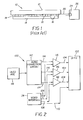
- Fig. 1 shows a cross section view of a typical prior art active matrix bottom emitting electroluminescent display such as an organic light emitting diode (OLED) flat panel display 10 of the type shown in US Patent 5,937,272, issued August 10, 1999 to Tang.
- the OLED display 10 includes a transparent substrate 12 that provides mechanical support for the display device, a transistor switching matrix layer 14, a light emission layer 18 containing materials forming organic light emitting diodes, and a cable 20 for connecting circuitry within the flat panel display to video interface circuit 24 , located on printed circuit board 26 .
- the transparent substrate 12 is typically glass, but other materials, such as plastic, may be used.
- the transistor switching matrix layer 14 contains a two-dimensional matrix of thin film transistors (TFTs) 16 that are used to select which pixel in the OLED display receives image data at a given time.
- TFTs thin film transistors
- the thin film transistors 16 are manufactured using conventional semiconductor manufacturing processes, and therefore extra thin film transistors 16 may be used to form circuitry for a variety of uses.
- the presence of TFTs within an active matrix flat panel display allows functions other than display to be implemented on the same substrate as the display function, producing a system-on-panel.
- the OLED display is responsive to digital control signals and analog video signals generated by video interface circuit 24 .
- organic light emitting materials undergo an aging process, where changes in the materials cause the light output of a given material for a constant input current stimulus to change with age. This causes a given image signal to produce a different image as the materials age.
- users of organic electroluminescent displays expect a given image signal to produce the same image, regardless of the ages of the organic light emitting materials.
- users may expect a given image signal to produce a pleasing image, although not necessarily the same image, regardless of the ages of the organic light emitting materials. For example, a dimmer image, but with proper color balance, may be acceptable, rather than the same, brighter image.
- the signal from the light sensor undergoes analog-to-digital conversion, and a processor calculates the measured light value and stores it.
- the display controller utilizes this stored luminance information to correct for non-uniformities in the light outputs from the pixels, which may occur due to aging.
- This method is complex because it requires a "pixel luminance map" that must store information regarding each pixel, or each area of pixels, which may require a lot of memory. This can be expensive to implement, particularly for portable devices, which are often price sensitive.
- the "pixel luminance map” memories must be updated periodically, and therefore must be either a volatile or a rewritable volatile memory. Volatile memories typically consume more power than non-volatile memories, in order to maintain their contents. Non-volatile memories such as FLASH consume less power when not being written, but have a limited number of update cycles prior to failure. Therefore, a "pixel luminance map" may be costly, power inefficient, and have limited life.
- a display that includes an electroluminescent display panel containing a light emitting material; a video interface circuit for producing an analog video signal for driving the display; an age circuit for supplying a signal representing the age of the light emitting material; an aging correction circuit responsive to the age signal for forming an analog aging correction signal, the aging correction circuit including, controller means responsive to the age signal for producing a digital correction value, and a digital to analog converter for converting the digital correction value to an analog correction signal; and a summing amplifier for summing the analog aging correction signal with the video signal.
- the display according to the present invention is advantageous in that it exhibits a near constant luminance and/or color balance for given analog video voltages as the light emitting materials of an electroluminescent display age.
- the circuit is optimized for compensating analog video channels, and therefore is simpler, more cost efficient, and benefits from higher manufacturing yields than previous methods.
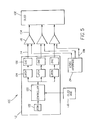
- an electroluminescent display system generally designated 100 includes an electroluminescent display panel 102 driven by one or more aging corrected analog video signals 104 .
- a video interface circuit 24 produces analog video signals 108 and control signals 110 .
- An aging correction circuit 112 is responsive to an electroluminescent display age input from an age circuit 118 , to produce analog correction signals 114.
- the analog correction signals are combined with the analog video signals 108 within summing amplifiers 116 .
- the electroluminescent display panel 102 contains light emitting materials. For multicolor displays, the light emitting materials that emit the different colors of light may age at different rates.
- an age for each color of light emitting materials is provided, since the light emitting materials for different colors age at different rates.
- a single overall age signal may be presented to a multiplicity of video channels when the light emitting materials of these video channels age similarly.
- the age circuit 118 may supply one average age of the light emitting materials, an average age of each light emitting material in a multicolor electroluminescent display, an average age of the light emitting material for subset areas of the active area, an average age of each light emitting material for subset areas of the active area, an average age of the light emitting materials for each pixel within the active area, or the age of each light emitting material at each pixel of the active area.
- the granularity of age measurement depends on a tradeoff between design complexity, cost, the profiles of the aging of the light emitting materials, and power consumption.
- age may be measured by counting the time the OLED has been driven.
- age may be indirectly measured by using a light detector to measure the actual light output of the electroluminescent display, and comparing it to the expected light output for the given drive conditions, as described in US Patent 6,081,073, referenced above. This light output may be taken from the display of normal images, or from test patterns displayed during inactive periods, as described by Salam, in his paper "OLED and LED Displays with Autonomous Pixel Matching," referenced above.
- Age may also be indirectly measured by using a reference pixel. In one method, the light output of a reference pixel formed within the electroluminescent display panel 102 emits light, and the light output is sensed, as described in US Patent 6,320,325, issued November 20, 2001 to Cok et al.
- the electrical characteristics of a reference pixel are measured.
- the measured electrical characteristic must change proportionally to the OLED material's age. This method is described in EP Application No. 01201792.7, filed May 14, 2001 by Cok et al.
- the age circuit 118 may produce a measured value that is related to age, rather than an actual chronological age.
- the aging correction circuit 112 then converts this measured value into a chronological actual age via a functional relationship.
- the aging correction circuit 112 contains a controller 120 , one or more memories 122 , one or more latches 124 , and one or more digital-to-analog converters 126 .
- the controller 120 may be implemented as custom digital logic, a programmed microprocessor, a microcontroller, or digital signal processor, and is responsive to age input from age circuit 118 .
- the memories 122 hold age correction information, where each memory address corresponds to a predetermined age, and the contents of each memory location contain a digital voltage difference based on the predetermined age. Thus, the memories 122 are used as correction value look-up tables.
- these memories 122 do not contain a "pixel luminance map," the size of the memories used in the current embodiment are typically much smaller than those used to store a pixel luminance map.
- the memories may be volatile or non-volatile. Volatile memories are useful for use with different electroluminescent display panels 102 having different aging characteristics, which occurs relatively often. However, volatile memories require initialization prior to use in aging correction. Alternatively, non-volatile memories are useful when the aging correction circuit 112 is normally operated with a single electroluminescent display, and therefore does not need initialization prior to every use.
- Non-volatile memories may be read-only memory (ROM), electrically programmable read-only memory (EPROM), electrically erasable programmable read-only memory (EEPROM), or FLASH memory.
- ROM read-only memory
- EPROM electrically programmable read-only memory
- EEPROM electrically erasable programmable read-only memory
- FLASH memory FLASH memory.
- the latter two types of memory are reprogrammable, and therefore allow for updates to the lookup table for better accuracy in the future, or for re-use of the circuitry with different devices or organic light emitting materials.
- the frequency of update is relatively low compared to the frequency of update of a "pixel luminance map," and therefore the number of write cycles for a FLASH device will usually not be a concern.
- Latches 124 are used to synchronize the digital aging correction value to the clock controlling the digital-to-analog converters 126 .
- the latches 124 may be omitted if this synchronization occurs inherently as a part of circuit operation, or if the memories 122 contain a latching function.
- the controller 120 Utilizing the input age, the controller 120 produces a corresponding memory address for the memories 122 .
- the address is sent to the memories 122, and corresponding digital aging correction values are read from these memories 122.
- latches 124 When present, latches 124 then latch these digital aging correction values.
- the digital-to-analog converters 126 then convert these digital aging correction values to analog form.
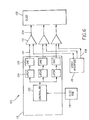
- Fig. 4 shows an embodiment of the present invention where the aging correction circuit 112 contains only one memory 122 , one latch 124 , and one digital-to-analog converter 126 .
- the output of the aging correction circuit 112 is combined with more than one video channel using summing amplifiers 116 .
- This embodiment is useful where two different light emitting materials exhibit the same, or relatively close, aging profiles, or where reduced complexity of the aging correction circuit 112 is desired.
- This embodiment has the advantages of being simple, thereby reducing cost, using fewer materials, and improving circuit yields.
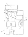
- Fig. 5 shows an embodiment of the present invention where the aging correction circuit 112 contains a single memory 122 , a controller 120 , one or more latches 124 , and one or more digital-to-analog converters 126 .
- Controller 120 is responsive to organic electroluminescent display age input 118 and reads appropriate aging-to-voltage correction data from memory 122 . When multiple color channels are present, the controller 120 computes the appropriate aging-to-voltage correction value for one color channel at a time, and stores this value in the appropriate latch 124. Once a new value is stored in latch 124, the corresponding digital-to-analog converter 126 converts this digital value to analog.
- Controller 120 synchronizes the look-up operation, latching, and the digital-to-analog conversion. Because the light emitting materials aging process is relatively slow (measured in hours) as compared to the look-up, computation, latching, and digital-to-analog conversion process using conventional clock periods (measured in hundreds of microseconds), this embodiment may be utilized to reduce the parts count in the circuit. Therefore, this embodiment reduces materials and cost, and improves yields over more complex embodiments.
- Fig. 6 shows an embodiment of the present invention where the aging correction circuit 112 contains controller 120 , one or more latches 124 , and one or more digital-to-analog converters 126 .
- This embodiment does not use a memory look-up table, but instead relies on a mathematical relationship to directly calculate an aging-to-voltage correction value via computations performed by controller 120 . Different mathematical relationships may be used for different light emitting materials within the organic electroluminescent display 102 .
- the digital age-to-voltage correction values are stored in latches 124 , and converted to analog voltages by digital-to-analog converters 126 .
- This embodiment is useful where the mathematical relationship between the age of the light emitting materials and light output is relatively simple and therefore does not require a very powerful controller for computation. Likewise, this embodiment is useful when the aging process of the materials is slow enough so that complex calculations may be performed over a relatively long period of time.
- This embodiment has the advantage of eliminating the memories associated with look-up tables, and therefore requires fewer materials, reduces cost, improves yields, and reduces manufacturing steps, since manufacturing processes associated with memories are often different from those associated with digital logic.
- Fig. 7 shows the conventional placement of the various elements of the electroluminescent display system 100 .
- OLED age circuit 118 the aging correction circuit 112 , the video interface circuit 24 , and the summing amplifiers 116 would be components mounted on a circuit board 30 .
- the aging corrected analog video signals 104 are then supplied to the organic electroluminescent display panel 102 via a cable 20 .
- the cable 20 connects to the printed circuit board 26 at connector 28 .
- circuitry may be integrated on the same substrate as an active matrix electroluminescent display. Therefore, all, or a part of the circuitry described herein with respect to aging correction may be implemented on the electroluminescent display's substrate.
- Fig. 8 shows the basic structure of such an electroluminescent display system 100 .
- Electroluminescent display panel 102 includes an active area 130 in which the light emitting materials and pixels of the electroluminescent display panel 102 are located. Additionally, since thin film transistors are located within the active area 130 , it is relatively simple to form additional circuitry 132 including additional thin film transistors around the periphery of the active area 130 .
- this circuitry 132 may be placed close to cable 20 , if it is responsive to signals carried over the cable 20 , and the output of the circuitry 132 is used to control circuitry within the active area 130.
- existing circuitry within active area 130 may be modified to include all of, or portion of, additional circuitry 132.
- Fig. 9 shows an embodiment of the present invention where the summing amplifiers 116 are physically located on the electroluminescent display panel 102 within circuitry 132 .
- the summing amplifiers 116 are placed around the periphery of the active area 130 .
- One or more analog correction signals 114, along with analog video signals 108 are transmitted over cable 20 to the electroluminescent display 102 .
- the summing amplifiers 116 easily integrate into the manufacturing process of the electroluminescent display panel 102 , since such analog circuitry is already formed within the electroluminescent display itself to accommodate the analog video channels.
- This embodiment has the advantage of reducing parts count on the printed circuit board 26, utilizing high density integration technology on the electroluminescent display panel 102, reducing overall system cost.
- Fig. 10 shows a further embodiment of the present invention where the latches 124 , the digital-to-analog converters 126 and the summing amplifiers 116 are physically located on the electroluminescent display 102 within circuitry 132 .
- the latches 124 , the digital-to-analog converters 126 , and the summing amplifiers 116 are placed around the periphery of the active area 130.
- the digital aging-to-color voltage correction output by the memories 122 on the printed circuit board 26 , along with analog video signals 108 are transmitted over cable 20 to the electroluminescent display panel 102 .
- a digital transmission circuit 136 performs a conversion of the digital aging-to-color voltage correction value to the transmission format.
- a digital receiver circuit 140 located within circuitry added to the electroluminescent display panel 102 , receives these transmitted correction values, and stores them in the appropriate latch 124 on the electroluminescent display panel 102.
- the digital aging-to-color voltage correction values are transmitted digitally over cable 20 .
- This digital transmission can utilize serial or parallel transmission format. Serial transmission is preferred, since fewer conductors are required, minimizing materials and therefore cost. Serial transmission is often slower than parallel transmission. However, since the aging rate of the light emitting materials is very slow in comparison to conventional serial transmission rates, it is normally acceptable to transmit at this lower rate.
- This embodiment has the advantage of reducing parts count on the printed circuit board 26 , utilizing high density integration technology on the electroluminescent display panel 102 , reducing overall system cost.
- Fig. 11 shows a further embodiment of the present invention where the memories 122 , latches 124 , the digital-to-analog converters 126 and the summing amplifiers 116 are physically located on the electroluminescent display panel 102 within circuitry 132.
- the memories 122, the latches 124 , the digital-to-analog converters 126 and the summing amplifiers 116 are placed around the periphery of the active area 130 .
- Controller 120 on the printed circuit board 26 computes the digital memory address values. These digital memory address values, along with analog video signals 108 , are transmitted over cable 20 to the electroluminescent display panel 102 .
- a digital transmission circuit 136 performs a conversion of the digital memory address values to the transmission format.
- a digital receiver circuit 140 located within circuitry added to the electroluminescent display panel 102 , receives these transmitted correction values, and routes them to the appropriate memories 122 on the electroluminescent display panel 102.
- This embodiment has the advantage of further reducing parts count on the printed circuit board 26 , utilizing high density integration technology on the electroluminescent display panel 102 , reducing overall system cost.
- Fig. 12 shows a further embodiment of the present invention where the entire aging correction circuit 112 , the electroluminescent display age input 118 , and the summing amplifiers 116 are physically located on the electroluminescent display panel 102 within circuitry 132 .
- aging correction circuit 112 , the organic electroluminescent display age input 118 , and the summing amplifiers 116 are placed around the periphery of the active area 130.
- the video interface circuit 24 remains on the printed circuit board 26 .
- This embodiment places the entire aging correction functionality on the electroluminescent display panel 102 itself, making the aging correction operation and manufacturing independent of the system designer.
- the integration of the aging correction circuit 112 , the electroluminescent display age input 118 , and the summing amplifiers 116 on the electroluminescent display panel 102 requires fewer components to be placed on the printed circuit board 26 , reducing circuit board materials and cost. Since no additional signals must be transmitted over connector 28 and cable 20, the same pinout may be used for an electroluminescent display with and without aging correction. This increases the flexibility of the electroluminescent display system 100 , and allows electroluminescent displays with and without aging correction to be used in the electroluminescent display system interchangeably.
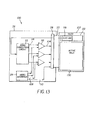
- Fig. 13 shows a further embodiment of the present invention where circuitry 132 on the electroluminescent display panel 102 includes the age circuit 118 .
- the age of the light emitting materials of the electroluminescent display panel 102 is supplied to the age correction circuit 112 located on printed circuit board 26 via one or more conductors in cable 20 .
- the placement of the age circuit 118 on the electroluminescent display panel 102 allows the measurement of materials age to be coupled to the electroluminescent display panel 102 , and not physically a part of circuitry external to the electroluminescent display panel 102 .
- a different electroluminescent display panel 102 can be plugged in to connector 28, and the age correction circuit 112 would operate correctly for this new display, within the need for reprogramming. This increases the usability of the electroluminescent display system 100 , decreasing integration costs, and allowing complex aging correction circuitry 112 to be implemented off of the display substrate and in integrated circuitry, where manufacturing yields are currently higher.
Landscapes
- Engineering & Computer Science (AREA)
- Physics & Mathematics (AREA)
- Computer Hardware Design (AREA)
- General Physics & Mathematics (AREA)
- Theoretical Computer Science (AREA)
- Electroluminescent Light Sources (AREA)
- Control Of Indicators Other Than Cathode Ray Tubes (AREA)
- Control Of El Displays (AREA)
Applications Claiming Priority (2)
| Application Number | Priority Date | Filing Date | Title |
|---|---|---|---|
| US940192 | 1992-09-02 | ||
| US09/940,192 US6501230B1 (en) | 2001-08-27 | 2001-08-27 | Display with aging correction circuit |
Publications (2)
| Publication Number | Publication Date |
|---|---|
| EP1291840A2 true EP1291840A2 (de) | 2003-03-12 |
| EP1291840A3 EP1291840A3 (de) | 2006-05-10 |
Family
ID=25474399
Family Applications (1)
| Application Number | Title | Priority Date | Filing Date |
|---|---|---|---|
| EP02078399A Withdrawn EP1291840A3 (de) | 2001-08-27 | 2002-08-15 | Anzeige mit Alterungs-Korrekturschaltung |
Country Status (5)
| Country | Link |
|---|---|
| US (1) | US6501230B1 (de) |
| EP (1) | EP1291840A3 (de) |
| JP (1) | JP2003151765A (de) |
| KR (1) | KR20030019103A (de) |
| TW (1) | TW591942B (de) |
Cited By (3)
| Publication number | Priority date | Publication date | Assignee | Title |
|---|---|---|---|---|
| EP1355289A3 (de) * | 2002-04-15 | 2005-06-08 | Pioneer Corporation | Steuervorrichtung mit Verschlechterungsfeststellung für eine selbstleuchtende Anzeigevorrichtung |
| EP2469505A1 (de) * | 2010-12-23 | 2012-06-27 | Research In Motion Limited | Tragbare elektronische Kommunikationsvorrichtung mit altersausgleichender Anzeige |
| US8514179B2 (en) | 2010-12-23 | 2013-08-20 | Research In Motion Limited | Handheld electronic communication device having an age compensating display |
Families Citing this family (68)
| Publication number | Priority date | Publication date | Assignee | Title |
|---|---|---|---|---|
| SG107573A1 (en) * | 2001-01-29 | 2004-12-29 | Semiconductor Energy Lab | Light emitting device |
| TWI248319B (en) | 2001-02-08 | 2006-01-21 | Semiconductor Energy Lab | Light emitting device and electronic equipment using the same |
| US6963321B2 (en) * | 2001-05-09 | 2005-11-08 | Clare Micronix Integrated Systems, Inc. | Method of providing pulse amplitude modulation for OLED display drivers |
| US6836260B2 (en) * | 2001-07-31 | 2004-12-28 | Eastman Kodak Company | Light emitting flat-panel display |
| AU2002326068A1 (en) * | 2001-08-23 | 2003-03-10 | Koninklijke Philips Electronics N.V. | Method and drive means for color correction in an organic electroluminescent device |
| US7027015B2 (en) * | 2001-08-31 | 2006-04-11 | Intel Corporation | Compensating organic light emitting device displays for color variations |
| SG120889A1 (en) * | 2001-09-28 | 2006-04-26 | Semiconductor Energy Lab | A light emitting device and electronic apparatus using the same |
| SG120888A1 (en) * | 2001-09-28 | 2006-04-26 | Semiconductor Energy Lab | A light emitting device and electronic apparatus using the same |
| US20030071821A1 (en) * | 2001-10-11 | 2003-04-17 | Sundahl Robert C. | Luminance compensation for emissive displays |
| JP2003255900A (ja) * | 2002-02-27 | 2003-09-10 | Sanyo Electric Co Ltd | カラー有機el表示装置 |
| US7170478B2 (en) * | 2002-03-26 | 2007-01-30 | Semiconductor Energy Laboratory Co., Ltd. | Method of driving light-emitting device |
| US6911781B2 (en) * | 2002-04-23 | 2005-06-28 | Semiconductor Energy Laboratory Co., Ltd. | Light emitting device and production system of the same |
| JP2003330419A (ja) * | 2002-05-15 | 2003-11-19 | Semiconductor Energy Lab Co Ltd | 表示装置 |
| US20040150594A1 (en) * | 2002-07-25 | 2004-08-05 | Semiconductor Energy Laboratory Co., Ltd. | Display device and drive method therefor |
| KR100528692B1 (ko) * | 2002-08-27 | 2005-11-15 | 엘지.필립스 엘시디 주식회사 | 유기전계발광소자용 에이징 회로 및 그 구동방법 |
| JP4865986B2 (ja) * | 2003-01-10 | 2012-02-01 | グローバル・オーエルイーディー・テクノロジー・リミテッド・ライアビリティ・カンパニー | 有機el表示装置 |
| EP1814100A3 (de) * | 2003-05-23 | 2008-03-05 | Barco, naamloze vennootschap. | Verfahren zur Anzeige von Bildern auf einer Grossbildschirmanzeige aus organischen Leuchtdioden sowie die dazu verwendete Anzeige |
| US20040257352A1 (en) * | 2003-06-18 | 2004-12-23 | Nuelight Corporation | Method and apparatus for controlling |
| WO2004111984A1 (en) * | 2003-06-19 | 2004-12-23 | Koninklijke Philips Electronics N.V. | Display system with impending failure indicator |
| JP4804711B2 (ja) * | 2003-11-21 | 2011-11-02 | 株式会社 日立ディスプレイズ | 画像表示装置 |
| DE10354820A1 (de) * | 2003-11-24 | 2005-06-02 | Ingenieurbüro Kienhöfer GmbH | Verfahren und Vorrichtung zum Betrieb eines verschleißbehafteten Displays |
| US7224332B2 (en) * | 2003-11-25 | 2007-05-29 | Eastman Kodak Company | Method of aging compensation in an OLED display |
| JP4855648B2 (ja) * | 2004-03-30 | 2012-01-18 | グローバル・オーエルイーディー・テクノロジー・リミテッド・ライアビリティ・カンパニー | 有機el表示装置 |
| US20050243023A1 (en) * | 2004-04-06 | 2005-11-03 | Damoder Reddy | Color filter integrated with sensor array for flat panel display |
| CN1981318A (zh) * | 2004-04-12 | 2007-06-13 | 彩光公司 | 用于有源矩阵发光显示器的低功耗电路及其控制方法 |
| US20050248515A1 (en) * | 2004-04-28 | 2005-11-10 | Naugler W E Jr | Stabilized active matrix emissive display |
| WO2005114630A1 (en) * | 2004-05-21 | 2005-12-01 | Semiconductor Energy Laboratory Co., Ltd. | Display device and electronic device |
| US7482629B2 (en) * | 2004-05-21 | 2009-01-27 | Semiconductor Energy Laboratory Co., Ltd. | Display device and electronic device |
| US7245297B2 (en) * | 2004-05-22 | 2007-07-17 | Semiconductor Energy Laboratory Co., Ltd. | Display device and electronic device |
| TWI238374B (en) * | 2004-06-17 | 2005-08-21 | Au Optronics Corp | Organic light emitting diode display, display luminance compensating device thereof, and compensating method thereof |
| JP4705764B2 (ja) * | 2004-07-14 | 2011-06-22 | 株式会社半導体エネルギー研究所 | ビデオデータ補正回路及び表示装置の制御回路並びにそれを内蔵した表示装置・電子機器 |
| US20060017669A1 (en) * | 2004-07-20 | 2006-01-26 | Eastman Kodak Company | Method and apparatus for uniformity and brightness correction in an OLED display |
| KR101246642B1 (ko) * | 2004-07-23 | 2013-03-25 | 가부시키가이샤 한도오따이 에네루기 켄큐쇼 | 표시 장치 및 이의 구동 방법 |
| US7540978B2 (en) | 2004-08-05 | 2009-06-02 | Novaled Ag | Use of an organic matrix material for producing an organic semiconductor material, organic semiconductor material and electronic component |
| JP4822387B2 (ja) * | 2004-08-31 | 2011-11-24 | 東北パイオニア株式会社 | 有機elパネルの駆動装置 |
| US20060044299A1 (en) * | 2004-08-31 | 2006-03-02 | Jian Wang | System and method for compensating for a fabrication artifact in an electronic device |
| US20060061292A1 (en) * | 2004-09-17 | 2006-03-23 | Samsung Electronics Co., Ltd. | Display device and driving method thereof |
| WO2006037363A1 (de) * | 2004-10-06 | 2006-04-13 | Fraunhofer-Gesellschaft zur Förderung der angewandten Forschung e.V. | Vorrichtung und verfahren zum ansteuern einer organischen leuchtdiode |
| DE602004006275T2 (de) | 2004-10-07 | 2007-12-20 | Novaled Ag | Verfahren zur Dotierung von einem Halbleitermaterial mit Cäsium |
| US7400345B2 (en) * | 2004-10-22 | 2008-07-15 | Eastman Kodak Company | OLED display with aspect ratio compensation |
| JP4934963B2 (ja) * | 2005-01-21 | 2012-05-23 | ソニー株式会社 | 焼き付き現象補正方法、自発光装置、焼き付き現象補正装置及びプログラム |
| US7450095B2 (en) * | 2005-03-24 | 2008-11-11 | Ownway Tech Corporation | Single-cluster lamp drive device |
| DE502005009415D1 (de) * | 2005-05-27 | 2010-05-27 | Novaled Ag | Transparente organische Leuchtdiode |
| EP1734793B1 (de) * | 2005-06-14 | 2008-04-16 | Novaled AG | Verfahren zum Betreiben eines organischen lichtemittierenden Bauteils und organisches lichtemittierendes Bauteil |
| KR100625642B1 (ko) * | 2005-06-30 | 2006-09-20 | 엘지.필립스 엘시디 주식회사 | 유기전계발광 표시장치 |
| JP5010814B2 (ja) * | 2005-07-07 | 2012-08-29 | グローバル・オーエルイーディー・テクノロジー・リミテッド・ライアビリティ・カンパニー | 有機el表示装置の製造方法 |
| DE102005042704A1 (de) * | 2005-09-01 | 2007-03-08 | Ingenieurbüro Kienhöfer GmbH | Verfahren zum Betreiben einer Anzeigevorrichtung mit einer Mehrzahl von verschleißbehafteten Bildelementen und Anzeigevorrichtung |
| US20070052632A1 (en) * | 2005-09-06 | 2007-03-08 | Chih-Liang Wu | Driving method which drives display units of different frequency spectra with respective sweep signals and apparatus based on the same |
| KR101166585B1 (ko) * | 2005-12-01 | 2012-07-18 | 엘지디스플레이 주식회사 | 정전기 방지를 위한 에이징패드를 구비한 평판표시소자 |
| US20080048951A1 (en) * | 2006-04-13 | 2008-02-28 | Naugler Walter E Jr | Method and apparatus for managing and uniformly maintaining pixel circuitry in a flat panel display |
| US20070290947A1 (en) * | 2006-06-16 | 2007-12-20 | Cok Ronald S | Method and apparatus for compensating aging of an electroluminescent display |
| US7696965B2 (en) * | 2006-06-16 | 2010-04-13 | Global Oled Technology Llc | Method and apparatus for compensating aging of OLED display |
| WO2008047271A2 (en) * | 2006-10-20 | 2008-04-24 | Philips Intellectual Property & Standards Gmbh | Organic light emitting diode device |
| US7928936B2 (en) * | 2006-11-28 | 2011-04-19 | Global Oled Technology Llc | Active matrix display compensating method |
| JP5317419B2 (ja) * | 2007-03-07 | 2013-10-16 | 株式会社ジャパンディスプレイ | 有機el表示装置 |
| US8077123B2 (en) * | 2007-03-20 | 2011-12-13 | Leadis Technology, Inc. | Emission control in aged active matrix OLED display using voltage ratio or current ratio with temperature compensation |
| JP2009025735A (ja) * | 2007-07-23 | 2009-02-05 | Hitachi Displays Ltd | 画像表示装置 |
| DE102007000881A1 (de) | 2007-11-12 | 2009-05-14 | Bundesdruckerei Gmbh | Dokument mit einer integrierten Anzeigevorrichtung, Verfahren zur Herstellung eines Dokuments und Lesegerät |
| US7679951B2 (en) * | 2007-12-21 | 2010-03-16 | Palo Alto Research Center Incorporated | Charge mapping memory array formed of materials with mutable electrical characteristics |
| ES2338962B1 (es) * | 2008-01-11 | 2011-04-04 | Senia Technologies S.L. | Configuracion de reguladores de corriente para pantallas de video flexibles a base de led's. |
| TW201006256A (en) * | 2008-07-16 | 2010-02-01 | Acer Inc | Automatic color adjustment method and automatic color adjustment device |
| CN103280188B (zh) * | 2013-06-14 | 2015-09-02 | 电子科技大学 | Oled器件老化补偿系统及方法 |
| US10839734B2 (en) * | 2013-12-23 | 2020-11-17 | Universal Display Corporation | OLED color tuning by driving mode variation |
| EP3067857A1 (de) * | 2015-03-13 | 2016-09-14 | Thomson Licensing | Verfahren und vorrichtung zur verarbeitung eines peripheriebildes |
| CA2886862A1 (en) * | 2015-04-01 | 2016-10-01 | Ignis Innovation Inc. | Adjusting display brightness for avoiding overheating and/or accelerated aging |
| CN106373535A (zh) * | 2016-08-26 | 2017-02-01 | 深圳市金立通信设备有限公司 | 一种屏幕颜色矫正方法及终端 |
| US10235962B2 (en) | 2016-12-23 | 2019-03-19 | Microsoft Technology Licensing, Llc | Techniques for robust reliability operation of a thin-film transistor (TFT) display |
| US10455653B1 (en) * | 2018-08-09 | 2019-10-22 | Innolux Corporation | LED driving circuits |
Family Cites Families (8)
| Publication number | Priority date | Publication date | Assignee | Title |
|---|---|---|---|---|
| US5093654A (en) * | 1989-05-17 | 1992-03-03 | Eldec Corporation | Thin-film electroluminescent display power supply system for providing regulated write voltages |
| JPH05260386A (ja) * | 1992-03-16 | 1993-10-08 | Sony Corp | 固体撮像素子の欠陥画素検出回路 |
| US6081073A (en) | 1995-12-19 | 2000-06-27 | Unisplay S.A. | Matrix display with matched solid-state pixels |
| JP4050802B2 (ja) * | 1996-08-02 | 2008-02-20 | シチズン電子株式会社 | カラー表示装置 |
| DE69825402T2 (de) * | 1997-03-12 | 2005-08-04 | Seiko Epson Corp. | Pixelschaltung, anzeigevorrichtung und elektronische apparatur mit stromgesteuerter lichtemittierender vorrichtung |
| US5937272A (en) | 1997-06-06 | 1999-08-10 | Eastman Kodak Company | Patterned organic layers in a full-color organic electroluminescent display array on a thin film transistor array substrate |
| US6897855B1 (en) | 1998-02-17 | 2005-05-24 | Sarnoff Corporation | Tiled electronic display structure |
| US6359398B1 (en) * | 1999-11-29 | 2002-03-19 | Mitsubishi Digital Electronics America Inc. | Method to control CRT phosphor aging |
-
2001
- 2001-08-27 US US09/940,192 patent/US6501230B1/en not_active Expired - Lifetime
-
2002
- 2002-07-10 TW TW091115339A patent/TW591942B/zh not_active IP Right Cessation
- 2002-08-15 EP EP02078399A patent/EP1291840A3/de not_active Withdrawn
- 2002-08-26 JP JP2002245711A patent/JP2003151765A/ja not_active Withdrawn
- 2002-08-26 KR KR1020020050452A patent/KR20030019103A/ko not_active Withdrawn
Cited By (4)
| Publication number | Priority date | Publication date | Assignee | Title |
|---|---|---|---|---|
| EP1355289A3 (de) * | 2002-04-15 | 2005-06-08 | Pioneer Corporation | Steuervorrichtung mit Verschlechterungsfeststellung für eine selbstleuchtende Anzeigevorrichtung |
| US7215307B2 (en) | 2002-04-15 | 2007-05-08 | Pioneer Corporation | Drive unit of self-luminous device with degradation detection function |
| EP2469505A1 (de) * | 2010-12-23 | 2012-06-27 | Research In Motion Limited | Tragbare elektronische Kommunikationsvorrichtung mit altersausgleichender Anzeige |
| US8514179B2 (en) | 2010-12-23 | 2013-08-20 | Research In Motion Limited | Handheld electronic communication device having an age compensating display |
Also Published As
| Publication number | Publication date |
|---|---|
| TW591942B (en) | 2004-06-11 |
| EP1291840A3 (de) | 2006-05-10 |
| JP2003151765A (ja) | 2003-05-23 |
| KR20030019103A (ko) | 2003-03-06 |
| US6501230B1 (en) | 2002-12-31 |
Similar Documents
| Publication | Publication Date | Title |
|---|---|---|
| US6501230B1 (en) | Display with aging correction circuit | |
| TWI415077B (zh) | 用以補償發光裝置顯示器之不均勻性的方法和系統 | |
| JP4865986B2 (ja) | 有機el表示装置 | |
| JP4855648B2 (ja) | 有機el表示装置 | |
| US10325554B2 (en) | OLED luminance degradation compensation | |
| US7262753B2 (en) | Method and system for measuring and controlling an OLED display element for improved lifetime and light output | |
| US7064733B2 (en) | Flat-panel display with luminance feedback | |
| US7164417B2 (en) | Dynamic controller for active-matrix displays | |
| EP2483885B1 (de) | Alterungskompensation eines elektrolumineszenzbauelements mit referenzsubpixeln | |
| US7986317B2 (en) | Organic light emitting display and driving method thereof, including compensating to display images of desired luminance | |
| US7321348B2 (en) | OLED display with aging compensation | |
| TWI385622B (zh) | 電致發光次像素補償驅動信號 | |
| US8077123B2 (en) | Emission control in aged active matrix OLED display using voltage ratio or current ratio with temperature compensation | |
| KR100885966B1 (ko) | 유기 발광 표시 장치 및 그 구동 방법 | |
| EP2453433B1 (de) | System und Verfahren zum Ausgleich von Ungleichförmigkeit in lichtemittierenden Vorrichtungsanzeigen | |
| JP2001092412A (ja) | アクティブマトリクス型表示装置 | |
| EP1260959A2 (de) | Anzeigetafel mit aktiver Matrix mit organischen Leuchtdioden | |
| KR20140083680A (ko) | 유기 발광 표시 장치 및 이의 구동 방법 | |
| KR20080090879A (ko) | 유기 전계 발광 표시 장치 및 그 구동 방법 | |
| JP2004348132A (ja) | 大画面有機発光ダイオードディスプレイに画像を表示する方法と該方法で使用するディスプレイ | |
| KR20080060146A (ko) | 액정 표시 장치 | |
| US20080231557A1 (en) | Emission control in aged active matrix oled display using voltage ratio or current ratio | |
| US20050023986A1 (en) | Organic EL display device with GAMMA correction | |
| CN101663697A (zh) | 用于有机电致发光面板的显示调整电路、显示调整电路和显示装置 | |
| KR20140026225A (ko) | 표시 장치 및 그 구동 방법 |
Legal Events
| Date | Code | Title | Description |
|---|---|---|---|
| PUAI | Public reference made under article 153(3) epc to a published international application that has entered the european phase |
Free format text: ORIGINAL CODE: 0009012 |
|
| AK | Designated contracting states |
Kind code of ref document: A2 Designated state(s): AT BE BG CH CY CZ DE DK EE ES FI FR GB GR IE IT LI LU MC NL PT SE SK TR Designated state(s): AT BE BG CH CY CZ DE DK EE ES FI FR GB GR IE IT LI LU MC NL PT SE SK TR |
|
| AX | Request for extension of the european patent |
Extension state: AL LT LV MK RO SI |
|
| PUAL | Search report despatched |
Free format text: ORIGINAL CODE: 0009013 |
|
| AK | Designated contracting states |
Kind code of ref document: A3 Designated state(s): AT BE BG CH CY CZ DE DK EE ES FI FR GB GR IE IT LI LU MC NL PT SE SK TR |
|
| AX | Request for extension of the european patent |
Extension state: AL LT LV MK RO SI |
|
| 17P | Request for examination filed |
Effective date: 20061009 |
|
| AKX | Designation fees paid |
Designated state(s): DE FR GB |
|
| 17Q | First examination report despatched |
Effective date: 20080519 |
|
| STAA | Information on the status of an ep patent application or granted ep patent |
Free format text: STATUS: THE APPLICATION IS DEEMED TO BE WITHDRAWN |
|
| 18D | Application deemed to be withdrawn |
Effective date: 20080930 |