EP1288846A2 - Leistungsverwaltung und Überstromdetektion für eine Fingeradruckerfassungsvorrichtung - Google Patents
Leistungsverwaltung und Überstromdetektion für eine Fingeradruckerfassungsvorrichtung Download PDFInfo
- Publication number
- EP1288846A2 EP1288846A2 EP02254952A EP02254952A EP1288846A2 EP 1288846 A2 EP1288846 A2 EP 1288846A2 EP 02254952 A EP02254952 A EP 02254952A EP 02254952 A EP02254952 A EP 02254952A EP 1288846 A2 EP1288846 A2 EP 1288846A2
- Authority
- EP
- European Patent Office
- Prior art keywords
- fingerprint sensor
- sensor circuitry
- heartbeat signal
- power management
- set forth
- Prior art date
- Legal status (The legal status is an assumption and is not a legal conclusion. Google has not performed a legal analysis and makes no representation as to the accuracy of the status listed.)
- Granted
Links
Images



Classifications
-
- G—PHYSICS
- G06—COMPUTING OR CALCULATING; COUNTING
- G06V—IMAGE OR VIDEO RECOGNITION OR UNDERSTANDING
- G06V40/00—Recognition of biometric, human-related or animal-related patterns in image or video data
- G06V40/10—Human or animal bodies, e.g. vehicle occupants or pedestrians; Body parts, e.g. hands
- G06V40/12—Fingerprints or palmprints
- G06V40/13—Sensors therefor
- G06V40/1329—Protecting the fingerprint sensor against damage caused by the finger
Definitions
- the present invention is directed, in general, to power management for integrated circuits and, more specifically, to power management with electrostatic discharge latchup event recovery for fingerprint sensor devices.
- Electrostatic discharge techniques normally employed for integrated circuits are often not entirely suitable or satisfactory for fingerprint sensor devices. Because such sensor devices must, of necessity, allow contact in proximity to the sensor circuitry, electrostatic discharge (ESD) protection to prevent latchup, circuit damage and other problems must be implemented in a different manner.
- ESD electrostatic discharge
- a primary requirement of power management for fingerprint sensor devices is the ability to restore operation of the fingerprint sensor circuitry following a latch-up condition triggered by an electrostatic discharge event.
- the same electrostatic discharge event occurring on the fingerprint sensor device and propagating inside the power management unit should not affect functionality of the power management unit.
- Fingerprint sensor devices may be required to operate at a nominal 5V supply), although optional operation at 3.3 volts supply may also be desired. Whether the dual power supply voltage capability accomplished by a charge pump receiving 3.3 volts and generating the 5 volt power supply voltage level or by a power regulator running out of 5 volts to produce both voltage levels, the power management unit should control the power of the charge pump or power regulator, if present, as well as shutting down the power supply of the fingerprint sensor device at will.
- a primary object of the present invention to provide, for use in a fingerprint detection system, a power management unit which monitors current drawn by a fingerprint sensor circuit and generates a "heartbeat" signal during normal operation. If a latchup event occurs, with attendant increase in current drawn by the fingerprint sensor circuitry, the heartbeat signal terminates and an interrupt is subsequently triggered to start a latchup recovery routine. Power to the fingerprint sensor circuitry is switched off and the interrupt is then cleared by writing appropriate values to control bits within the power management register.
- controller means any device, system or part thereof that controls at least one operation, whether such a device is implemented in hardware, firmware, software or some combination of at least two of the same. It should be noted that the functionality associated with any particular controller may be centralized or distributed, whether locally or remotely. Definitions for certain words and phrases are provided throughout this patent document, and those of ordinary skill in the art will understand that such definitions apply in many, if not most, instances to prior as well as future uses of such defined words and phrases.
- FIGURES 1 through 4 discussed below, and the various embodiments used to describe the principles of the present invention in this patent document are by way of illustration only and should not be construed in any way to limit the scope of the invention. Those skilled in the art will understand that the principles of the present invention may be implemented in any suitably arranged device.
- FIGURE 1 depicts a power management system for a fingerprint sensor device according to one embodiment of the present invention.
- Power management unit 100 an error check and correction (ECC) device, controls power flow from a power supply HV through an internal power switch 101.
- Power supply HV may be either a 5 volt or 3.3 volt power source.
- ECC error check and correction
- heartbeat unit ECG detects the attendant voltage drop increase between nodes P2 and P3.
- heartbeat unit ECG outputs a square wave synchronous with the system clock (the "heartbeat") when the fingerprint sensor device is powered and draws only the nominal current associated with normal operation.
- This heartbeat signal is rectified by diode D and filtered through a low pass filter LPF to provide a logical high or 1 signal at node P4 during normal operation.
- the heartbeat unit ECG output stops "beating,” providing, eventually, a logical low or zero output.
- node P4 gradually discharges to the ground voltage, asserting the interrupt signal INT output at logic gate 103, assuming the interrupt enable bit X is- on (a logical 1) and the power switch bit Y is also on.
- the interrupt signal is passed to the fingerprint sensor device 102 and/or any processor or controller controlling operation of the fingerprint sensor device 102 to initiate a reset or latchup recovery routine.
- Grounding of node P4 also causes a bus interface 104 for the fingerprint sensing device 102, , to ground the data bus 105 coupled to the fingerprint sensing device.
- the signal at node P4 may also be optionally routed, through the interrupt signal INT, to drive directly an ECC reset input for the fingerprint sensing device 102 and/or any associated processor or controller, starting a latchup recovery routine.
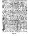
- FIGURES 2 and 3 are each a series of related plots illustrating operation of a power management system for a fingerprint sensor device according to one embodiment of the present invention, and specifically the power management unit 100 depicted in FIGURE 1.
- the top graph represents current through the sensing resistor R.
- ns nanoseconds
- 600 ns a latchup event is simulated, causing the current through sensing resistor R to increase to a high direct current (DC) value of 120 milliamps (mA) in the example shown.
- DC direct current
- mA milliamps
- the middle graph shows the corresponding output of the heartbeat unit ECG at node P1, as well as the signal at node P4. Activity at node P1 stops as soon as a latchup event occurs. After approximately 400 ns, node P4--which is the signal used to recover from the latchup event--goes to zero. The bottom graph shows the corresponding power supply voltage signal.
- FIGURE 3 shows a complete sequence of latchup and recovery.
- the top graph shows current through the sensing resistor R, with a latchup event occurring at about 600 ns with peak current of 80 mA.
- the bottom graph illustrates the corresponding signal at node P4, while the middle graph illustrates the voltages across sensing resistor R (at nodes P2 and P3) and the power control bit Y command to open the power switch 101.
- nodes P2 and P3 gradually discharge, causing a false transition to logic state 1 for node P4 but not affecting the operation since the interrupt signal INT has already been asserted.
- the latchup recovery routine triggered by the interrupt signal INT includes the following sequence of events, programmed into a read-only memory (ROM) within the ECC unit: (1) the fingerprint sensor power switch 101 is turned off by the power switch control bit Y within the power management unit 100; (2) the fingerprint sensor data lines are automatically grounded by the bus interface 104; and (3) after an appropriate delay, the startup sequence is launched.
- ROM read-only memory
- the startup sequence in the exemplary embodiment is controlled by a boot program and includes a zero logic state for the power control bit Y, leaving power control switch 101 temporarily open, with the interrupt signal INT being disabled through the enable interrupt control bit X.
- These states are necessary since the heartbeat unit ECG would not produce a heartbeat while there is no power supplied to nodes P2 and P3.
- the power switch 101 is closed and, after an appropriate delay, the interrupt signal INT is enabled by writing a logic one to the interrupt enable control bit X.
- FIGURE 4 depicts in greater detail control of an interrupt signal within a power management system for a fingerprint sensor device according to one embodiment of the present invention.
- Logic gate 103 receives the inverted state of node P4 and the pwr_switch_en signal corresponding to the power switch enable bit Y within the power management register.
- Logic gate 110 receives the raw_interrupt signal output of logic gate 103 and an early_interrupt signal from the output of a first flip-flop 112.
- Logic gate 111 receives the set_interrupt signal output by logic gate 110 and an interrupt_enable signal corresponding to interrupt enable bit X within th power management register.
- Logic gate 113 also receives the interrupt_enable signal and the output of edge-triggered flip-flop 112 reflecting whether node P4 has discharged to ground (before transitioning to a false logic one as described above).
- Edge-triggered flip-flop 114 generates the power management interrupt signal pwr_mgmt_int.
- the system reset clears the pwr_mgmt_int signal by writing zeros to the X and Y control bits of the power management register.
- the power switch 101 When the power switch 101 is turned on by writing a logical 1 into control bit Y and subsequently enabling the interrupt by writing a logical 1 into control bit X, the circuit is ready to detect a change from high to low of node P4, caused by a latchup event in the fingerprint sensor device.
- this transition is latched into pwr_mgmt_int.
- the routine responding to the interrupt after taking care to ground the data bus lines, will turn the power switch 101 off by writing a zero into control bit Y, and will eventually clear the interrupt by writing a zero in control bit X.
Landscapes
- Engineering & Computer Science (AREA)
- Human Computer Interaction (AREA)
- Physics & Mathematics (AREA)
- General Physics & Mathematics (AREA)
- Multimedia (AREA)
- Theoretical Computer Science (AREA)
- Image Input (AREA)
- Measurement Of The Respiration, Hearing Ability, Form, And Blood Characteristics Of Living Organisms (AREA)
- Measurement Of Length, Angles, Or The Like Using Electric Or Magnetic Means (AREA)
Applications Claiming Priority (2)
| Application Number | Priority Date | Filing Date | Title |
|---|---|---|---|
| US920530 | 2001-07-31 | ||
| US09/920,530 US6597289B2 (en) | 2001-07-31 | 2001-07-31 | Fingerprint sensor power management detection of overcurrent |
Publications (3)
| Publication Number | Publication Date |
|---|---|
| EP1288846A2 true EP1288846A2 (de) | 2003-03-05 |
| EP1288846A3 EP1288846A3 (de) | 2006-11-29 |
| EP1288846B1 EP1288846B1 (de) | 2007-10-31 |
Family
ID=25443901
Family Applications (1)
| Application Number | Title | Priority Date | Filing Date |
|---|---|---|---|
| EP02254952A Expired - Lifetime EP1288846B1 (de) | 2001-07-31 | 2002-07-15 | Leistungsverwaltung und Überstromdetektion für eine Fingeradruckerfassungsvorrichtung |
Country Status (4)
| Country | Link |
|---|---|
| US (1) | US6597289B2 (de) |
| EP (1) | EP1288846B1 (de) |
| JP (1) | JP4469127B2 (de) |
| DE (1) | DE60223207T2 (de) |
Families Citing this family (52)
| Publication number | Priority date | Publication date | Assignee | Title |
|---|---|---|---|---|
| US7474772B2 (en) | 2003-06-25 | 2009-01-06 | Atrua Technologies, Inc. | System and method for a miniature user input device |
| US7587072B2 (en) | 2003-08-22 | 2009-09-08 | Authentec, Inc. | System for and method of generating rotational inputs |
| US7697729B2 (en) | 2004-01-29 | 2010-04-13 | Authentec, Inc. | System for and method of finger initiated actions |
| US8131026B2 (en) | 2004-04-16 | 2012-03-06 | Validity Sensors, Inc. | Method and apparatus for fingerprint image reconstruction |
| US8229184B2 (en) | 2004-04-16 | 2012-07-24 | Validity Sensors, Inc. | Method and algorithm for accurate finger motion tracking |
| US8165355B2 (en) | 2006-09-11 | 2012-04-24 | Validity Sensors, Inc. | Method and apparatus for fingerprint motion tracking using an in-line array for use in navigation applications |
| US8358815B2 (en) | 2004-04-16 | 2013-01-22 | Validity Sensors, Inc. | Method and apparatus for two-dimensional finger motion tracking and control |
| US8175345B2 (en) | 2004-04-16 | 2012-05-08 | Validity Sensors, Inc. | Unitized ergonomic two-dimensional fingerprint motion tracking device and method |
| US8447077B2 (en) | 2006-09-11 | 2013-05-21 | Validity Sensors, Inc. | Method and apparatus for fingerprint motion tracking using an in-line array |
| WO2005106774A2 (en) | 2004-04-23 | 2005-11-10 | Validity Sensors, Inc. | Methods and apparatus for acquiring a swiped fingerprint image |
| DE602005022900D1 (de) * | 2004-10-04 | 2010-09-23 | Validity Sensors Inc | Fingerabdruckerfassende konstruktionen mit einem substrat |
| US7831070B1 (en) | 2005-02-18 | 2010-11-09 | Authentec, Inc. | Dynamic finger detection mechanism for a fingerprint sensor |
| JP2006301817A (ja) * | 2005-04-18 | 2006-11-02 | Toshiba Corp | 情報処理装置および制御方法 |
| US7660711B2 (en) * | 2006-04-28 | 2010-02-09 | Saudi Arabian Oil Company | Automated event monitoring system for online reservoir simulation |
| US8107212B2 (en) | 2007-04-30 | 2012-01-31 | Validity Sensors, Inc. | Apparatus and method for protecting fingerprint sensing circuitry from electrostatic discharge |
| US8276816B2 (en) | 2007-12-14 | 2012-10-02 | Validity Sensors, Inc. | Smart card system with ergonomic fingerprint sensor and method of using |
| US8204281B2 (en) | 2007-12-14 | 2012-06-19 | Validity Sensors, Inc. | System and method to remove artifacts from fingerprint sensor scans |
| US8116540B2 (en) | 2008-04-04 | 2012-02-14 | Validity Sensors, Inc. | Apparatus and method for reducing noise in fingerprint sensing circuits |
| EP2321764A4 (de) | 2008-07-22 | 2012-10-10 | Validity Sensors Inc | System, vorrichtung und verfahren zur sicherung einer gerätekomponente |
| US8391568B2 (en) | 2008-11-10 | 2013-03-05 | Validity Sensors, Inc. | System and method for improved scanning of fingerprint edges |
| US8278946B2 (en) | 2009-01-15 | 2012-10-02 | Validity Sensors, Inc. | Apparatus and method for detecting finger activity on a fingerprint sensor |
| US8600122B2 (en) | 2009-01-15 | 2013-12-03 | Validity Sensors, Inc. | Apparatus and method for culling substantially redundant data in fingerprint sensing circuits |
| US8374407B2 (en) | 2009-01-28 | 2013-02-12 | Validity Sensors, Inc. | Live finger detection |
| US9336428B2 (en) | 2009-10-30 | 2016-05-10 | Synaptics Incorporated | Integrated fingerprint sensor and display |
| US9400911B2 (en) | 2009-10-30 | 2016-07-26 | Synaptics Incorporated | Fingerprint sensor and integratable electronic display |
| US9274553B2 (en) | 2009-10-30 | 2016-03-01 | Synaptics Incorporated | Fingerprint sensor and integratable electronic display |
| US8866347B2 (en) | 2010-01-15 | 2014-10-21 | Idex Asa | Biometric image sensing |
| US8421890B2 (en) | 2010-01-15 | 2013-04-16 | Picofield Technologies, Inc. | Electronic imager using an impedance sensor grid array and method of making |
| US8791792B2 (en) | 2010-01-15 | 2014-07-29 | Idex Asa | Electronic imager using an impedance sensor grid array mounted on or about a switch and method of making |
| US9666635B2 (en) | 2010-02-19 | 2017-05-30 | Synaptics Incorporated | Fingerprint sensing circuit |
| US8716613B2 (en) | 2010-03-02 | 2014-05-06 | Synaptics Incoporated | Apparatus and method for electrostatic discharge protection |
| US9001040B2 (en) | 2010-06-02 | 2015-04-07 | Synaptics Incorporated | Integrated fingerprint sensor and navigation device |
| US8331096B2 (en) | 2010-08-20 | 2012-12-11 | Validity Sensors, Inc. | Fingerprint acquisition expansion card apparatus |
| EP2625649B1 (de) | 2010-10-08 | 2014-07-16 | Apple Inc. | Fingerabtastvorrichtung mit differenzmessungsschaltung und zugehörige verfahren |
| US8594393B2 (en) | 2011-01-26 | 2013-11-26 | Validity Sensors | System for and method of image reconstruction with dual line scanner using line counts |
| US8538097B2 (en) | 2011-01-26 | 2013-09-17 | Validity Sensors, Inc. | User input utilizing dual line scanner apparatus and method |
| GB2489100A (en) | 2011-03-16 | 2012-09-19 | Validity Sensors Inc | Wafer-level packaging for a fingerprint sensor |
| US10043052B2 (en) | 2011-10-27 | 2018-08-07 | Synaptics Incorporated | Electronic device packages and methods |
| US9195877B2 (en) | 2011-12-23 | 2015-11-24 | Synaptics Incorporated | Methods and devices for capacitive image sensing |
| US9785299B2 (en) | 2012-01-03 | 2017-10-10 | Synaptics Incorporated | Structures and manufacturing methods for glass covered electronic devices |
| US9137438B2 (en) | 2012-03-27 | 2015-09-15 | Synaptics Incorporated | Biometric object sensor and method |
| US9268991B2 (en) | 2012-03-27 | 2016-02-23 | Synaptics Incorporated | Method of and system for enrolling and matching biometric data |
| US9251329B2 (en) | 2012-03-27 | 2016-02-02 | Synaptics Incorporated | Button depress wakeup and wakeup strategy |
| US9600709B2 (en) | 2012-03-28 | 2017-03-21 | Synaptics Incorporated | Methods and systems for enrolling biometric data |
| US9152838B2 (en) | 2012-03-29 | 2015-10-06 | Synaptics Incorporated | Fingerprint sensor packagings and methods |
| WO2013155224A1 (en) | 2012-04-10 | 2013-10-17 | Picofield Technologies Inc. | Biometric sensing |
| US9665762B2 (en) | 2013-01-11 | 2017-05-30 | Synaptics Incorporated | Tiered wakeup strategy |
| KR102126816B1 (ko) | 2013-09-09 | 2020-07-08 | 삼성전자주식회사 | 지문 인식 장치 및 방법 |
| CN109359571B (zh) * | 2014-11-14 | 2022-08-12 | 深圳市汇顶科技股份有限公司 | 基于状态监视和握手的指纹传感器的闩锁恢复机制 |
| US10162996B2 (en) * | 2014-11-14 | 2018-12-25 | Shenzhen GOODIX Technology Co., Ltd. | Latchup recovery mechanism for fingerprint sensor based on state monitor and handshake |
| CN105302278B (zh) | 2015-10-19 | 2018-08-03 | 广东欧珀移动通信有限公司 | 指纹传感器串行外设接口的控制方法及装置和移动终端 |
| CN117175498B (zh) * | 2023-11-03 | 2024-03-22 | 深圳贝特莱电子科技股份有限公司 | 一种智能门锁指纹传感器保护电路及方法 |
Family Cites Families (6)
| Publication number | Priority date | Publication date | Assignee | Title |
|---|---|---|---|---|
| US6098330A (en) * | 1997-05-16 | 2000-08-08 | Authentec, Inc. | Machine including vibration and shock resistant fingerprint sensor and related methods |
| US6408087B1 (en) * | 1998-01-13 | 2002-06-18 | Stmicroelectronics, Inc. | Capacitive semiconductor user input device |
| US6091082A (en) * | 1998-02-17 | 2000-07-18 | Stmicroelectronics, Inc. | Electrostatic discharge protection for integrated circuit sensor passivation |
| US6346739B1 (en) * | 1998-12-30 | 2002-02-12 | Stmicroelectronics, Inc. | Static charge dissipation pads for sensors |
| US6628812B1 (en) * | 1999-05-11 | 2003-09-30 | Authentec, Inc. | Fingerprint sensor package having enhanced electrostatic discharge protection and associated methods |
| GB9922572D0 (en) * | 1999-09-24 | 1999-11-24 | Koninkl Philips Electronics Nv | Capacitive sensing array devices |
-
2001
- 2001-07-31 US US09/920,530 patent/US6597289B2/en not_active Expired - Lifetime
-
2002
- 2002-07-15 EP EP02254952A patent/EP1288846B1/de not_active Expired - Lifetime
- 2002-07-15 DE DE60223207T patent/DE60223207T2/de not_active Expired - Lifetime
- 2002-07-31 JP JP2002223040A patent/JP4469127B2/ja not_active Expired - Fee Related
Also Published As
| Publication number | Publication date |
|---|---|
| JP4469127B2 (ja) | 2010-05-26 |
| EP1288846A3 (de) | 2006-11-29 |
| US6597289B2 (en) | 2003-07-22 |
| JP2003175018A (ja) | 2003-06-24 |
| DE60223207D1 (de) | 2007-12-13 |
| US20030025606A1 (en) | 2003-02-06 |
| DE60223207T2 (de) | 2008-08-14 |
| EP1288846B1 (de) | 2007-10-31 |
Similar Documents
| Publication | Publication Date | Title |
|---|---|---|
| EP1288846B1 (de) | Leistungsverwaltung und Überstromdetektion für eine Fingeradruckerfassungsvorrichtung | |
| JP5977920B2 (ja) | パワーコンバータの入力端子電圧放電回路を実現する方法および装置 | |
| CA2210024C (en) | Method and apparatus for power supply switching with logic integrity protection | |
| US7295051B2 (en) | System and method for monitoring a power supply level | |
| US6664792B1 (en) | Method and apparatus for battery power pre-check at system power-on | |
| CA1162648A (en) | Low-power battery backup circuit for semiconductor memory | |
| US6274949B1 (en) | Back-up power accessory for a computer | |
| KR19990043981A (ko) | 파워-다운 리셋회로 | |
| US4337524A (en) | Backup power circuit for biasing bit lines of a static semiconductor memory | |
| US20080012603A1 (en) | Brown out detector | |
| JPH05173674A (ja) | グローバル・リセット回路 | |
| JP2002218645A (ja) | 電源保護回路及びリムーバブルディスク装置 | |
| US20150381164A9 (en) | Method for operating a backup circuit and circuit therefor | |
| CN100409369C (zh) | 电压检测电路控制设备及其存储器控制设备和存储卡 | |
| JP4077524B2 (ja) | パッド・ドライバ回路及びパッド・ドライバ回路を備えた電子回路 | |
| CN112269463A (zh) | 一种掉电保护电路、方法及电能表 | |
| EP4280031A1 (de) | Robustes ausfallsicheres system zur verlängerung der reservebatterielebensdauer in echtzeit-mcu-systemen mit niedriger leistung | |
| CN100413216C (zh) | 监控电源电压的电路装置 | |
| JP2002233079A (ja) | 無停電性スイッチングレギュレータ | |
| JP2780567B2 (ja) | 集積回路の給電装置 | |
| US20030039085A1 (en) | ESD protection circuit for multi-power and mixed-voltage integrated circuit | |
| JP2003318271A (ja) | 半導体集積回路 | |
| CN119154222A (zh) | 用于外置功率管的保护电路、实现方法及充电芯片 | |
| KR101802177B1 (ko) | 소형 셀에서의 프로세서 부팅을 위한 장치 및 방법 | |
| KR950007110B1 (ko) | 노트북 컴퓨터와 도킹 시스템의 전원 공급 장치 |
Legal Events
| Date | Code | Title | Description |
|---|---|---|---|
| PUAI | Public reference made under article 153(3) epc to a published international application that has entered the european phase |
Free format text: ORIGINAL CODE: 0009012 |
|
| AK | Designated contracting states |
Kind code of ref document: A2 Designated state(s): AT BE BG CH CY CZ DE DK EE ES FI FR GB GR IE IT LI LU MC NL PT SE SK TR |
|
| AX | Request for extension of the european patent |
Extension state: AL LT LV MK RO SI |
|
| RAP1 | Party data changed (applicant data changed or rights of an application transferred) |
Owner name: UPEK INC., |
|
| PUAL | Search report despatched |
Free format text: ORIGINAL CODE: 0009013 |
|
| AK | Designated contracting states |
Kind code of ref document: A3 Designated state(s): AT BE BG CH CY CZ DE DK EE ES FI FR GB GR IE IT LI LU MC NL PT SE SK TR |
|
| AX | Request for extension of the european patent |
Extension state: AL LT LV MK RO SI |
|
| 17P | Request for examination filed |
Effective date: 20070215 |
|
| GRAP | Despatch of communication of intention to grant a patent |
Free format text: ORIGINAL CODE: EPIDOSNIGR1 |
|
| RIC1 | Information provided on ipc code assigned before grant |
Ipc: G06K 9/00 20060101AFI20070531BHEP |
|
| RAP1 | Party data changed (applicant data changed or rights of an application transferred) |
Owner name: UPEK, INC. |
|
| AKX | Designation fees paid |
Designated state(s): DE FR GB IT |
|
| GRAS | Grant fee paid |
Free format text: ORIGINAL CODE: EPIDOSNIGR3 |
|
| GRAA | (expected) grant |
Free format text: ORIGINAL CODE: 0009210 |
|
| AK | Designated contracting states |
Kind code of ref document: B1 Designated state(s): DE FR GB IT |
|
| REG | Reference to a national code |
Ref country code: GB Ref legal event code: FG4D |
|
| REF | Corresponds to: |
Ref document number: 60223207 Country of ref document: DE Date of ref document: 20071213 Kind code of ref document: P |
|
| ET | Fr: translation filed | ||
| PLBE | No opposition filed within time limit |
Free format text: ORIGINAL CODE: 0009261 |
|
| STAA | Information on the status of an ep patent application or granted ep patent |
Free format text: STATUS: NO OPPOSITION FILED WITHIN TIME LIMIT |
|
| 26N | No opposition filed |
Effective date: 20080801 |
|
| REG | Reference to a national code |
Ref country code: FR Ref legal event code: CA |
|
| PGFP | Annual fee paid to national office [announced via postgrant information from national office to epo] |
Ref country code: IT Payment date: 20100714 Year of fee payment: 9 |
|
| PG25 | Lapsed in a contracting state [announced via postgrant information from national office to epo] |
Ref country code: IT Free format text: LAPSE BECAUSE OF NON-PAYMENT OF DUE FEES Effective date: 20110715 |
|
| REG | Reference to a national code |
Ref country code: GB Ref legal event code: 732E Free format text: REGISTERED BETWEEN 20120913 AND 20120919 |
|
| REG | Reference to a national code |
Ref country code: FR Ref legal event code: TP Owner name: AUTHENTEC, INC., US Effective date: 20121001 |
|
| REG | Reference to a national code |
Ref country code: DE Ref legal event code: R082 Ref document number: 60223207 Country of ref document: DE Representative=s name: SCHWABE SANDMAIR MARX, DE |
|
| REG | Reference to a national code |
Ref country code: DE Ref legal event code: R081 Ref document number: 60223207 Country of ref document: DE Owner name: AUTHENTEC, INC. (N.D.GES.D.STAATES DELAWARE), , US Free format text: FORMER OWNER: UPEK, INC., EMERYVILLE, CALIF., US Effective date: 20130528 Ref country code: DE Ref legal event code: R082 Ref document number: 60223207 Country of ref document: DE Representative=s name: BARDEHLE PAGENBERG PARTNERSCHAFT MBB PATENTANW, DE Effective date: 20130528 Ref country code: DE Ref legal event code: R081 Ref document number: 60223207 Country of ref document: DE Owner name: APPLE INC., CUPERTINO, US Free format text: FORMER OWNER: UPEK, INC., EMERYVILLE, CALIF., US Effective date: 20130528 Ref country code: DE Ref legal event code: R081 Ref document number: 60223207 Country of ref document: DE Owner name: AUTHENTEC, INC. (N.D.GES.D.STAATES DELAWARE), US Free format text: FORMER OWNER: UPEK, INC., EMERYVILLE, US Effective date: 20130528 Ref country code: DE Ref legal event code: R082 Ref document number: 60223207 Country of ref document: DE Representative=s name: SCHWABE SANDMAIR MARX, DE Effective date: 20130528 |
|
| REG | Reference to a national code |
Ref country code: FR Ref legal event code: PLFP Year of fee payment: 14 |
|
| REG | Reference to a national code |
Ref country code: FR Ref legal event code: PLFP Year of fee payment: 15 |
|
| REG | Reference to a national code |
Ref country code: FR Ref legal event code: TP Owner name: APPLE INC., US Effective date: 20160531 |
|
| REG | Reference to a national code |
Ref country code: DE Ref legal event code: R082 Ref document number: 60223207 Country of ref document: DE Representative=s name: BARDEHLE PAGENBERG PARTNERSCHAFT MBB PATENTANW, DE Ref country code: DE Ref legal event code: R081 Ref document number: 60223207 Country of ref document: DE Owner name: APPLE INC., CUPERTINO, US Free format text: FORMER OWNER: AUTHENTEC, INC. (N.D.GES.D.STAATES DELAWARE), MELBOURNE, FLA., US |
|
| REG | Reference to a national code |
Ref country code: GB Ref legal event code: 732E Free format text: REGISTERED BETWEEN 20160901 AND 20160907 |
|
| REG | Reference to a national code |
Ref country code: FR Ref legal event code: PLFP Year of fee payment: 16 |
|
| PGFP | Annual fee paid to national office [announced via postgrant information from national office to epo] |
Ref country code: FR Payment date: 20170613 Year of fee payment: 16 |
|
| PGFP | Annual fee paid to national office [announced via postgrant information from national office to epo] |
Ref country code: GB Payment date: 20170712 Year of fee payment: 16 Ref country code: DE Payment date: 20170711 Year of fee payment: 16 |
|
| REG | Reference to a national code |
Ref country code: DE Ref legal event code: R119 Ref document number: 60223207 Country of ref document: DE |
|
| GBPC | Gb: european patent ceased through non-payment of renewal fee |
Effective date: 20180715 |
|
| PG25 | Lapsed in a contracting state [announced via postgrant information from national office to epo] |
Ref country code: GB Free format text: LAPSE BECAUSE OF NON-PAYMENT OF DUE FEES Effective date: 20180715 Ref country code: FR Free format text: LAPSE BECAUSE OF NON-PAYMENT OF DUE FEES Effective date: 20180731 Ref country code: DE Free format text: LAPSE BECAUSE OF NON-PAYMENT OF DUE FEES Effective date: 20190201 |