EP1283662A1 - It laminating double-side circuit board and production method therefor and multi-layer printed circuit board using - Google Patents
It laminating double-side circuit board and production method therefor and multi-layer printed circuit board using Download PDFInfo
- Publication number
- EP1283662A1 EP1283662A1 EP02710365A EP02710365A EP1283662A1 EP 1283662 A1 EP1283662 A1 EP 1283662A1 EP 02710365 A EP02710365 A EP 02710365A EP 02710365 A EP02710365 A EP 02710365A EP 1283662 A1 EP1283662 A1 EP 1283662A1
- Authority
- EP
- European Patent Office
- Prior art keywords
- side circuit
- circuit board
- prepreg
- laminating double
- insulated substrate
- Prior art date
- Legal status (The legal status is an assumption and is not a legal conclusion. Google has not performed a legal analysis and makes no representation as to the accuracy of the status listed.)
- Withdrawn
Links
Images


Classifications
-
- H—ELECTRICITY
- H05—ELECTRIC TECHNIQUES NOT OTHERWISE PROVIDED FOR
- H05K—PRINTED CIRCUITS; CASINGS OR CONSTRUCTIONAL DETAILS OF ELECTRIC APPARATUS; MANUFACTURE OF ASSEMBLAGES OF ELECTRICAL COMPONENTS
- H05K3/00—Apparatus or processes for manufacturing printed circuits
- H05K3/46—Manufacturing multilayer circuits
- H05K3/4611—Manufacturing multilayer circuits by laminating two or more circuit boards
- H05K3/4614—Manufacturing multilayer circuits by laminating two or more circuit boards the electrical connections between the circuit boards being made during lamination
- H05K3/462—Manufacturing multilayer circuits by laminating two or more circuit boards the electrical connections between the circuit boards being made during lamination characterized by laminating only or mainly similar double-sided circuit boards
-
- H—ELECTRICITY
- H05—ELECTRIC TECHNIQUES NOT OTHERWISE PROVIDED FOR
- H05K—PRINTED CIRCUITS; CASINGS OR CONSTRUCTIONAL DETAILS OF ELECTRIC APPARATUS; MANUFACTURE OF ASSEMBLAGES OF ELECTRICAL COMPONENTS
- H05K3/00—Apparatus or processes for manufacturing printed circuits
- H05K3/0011—Working of insulating substrates or insulating layers
- H05K3/0017—Etching of the substrate by chemical or physical means
- H05K3/0026—Etching of the substrate by chemical or physical means by laser ablation
- H05K3/0032—Etching of the substrate by chemical or physical means by laser ablation of organic insulating material
- H05K3/0038—Etching of the substrate by chemical or physical means by laser ablation of organic insulating material combined with laser drilling through a metal layer
-
- H—ELECTRICITY
- H05—ELECTRIC TECHNIQUES NOT OTHERWISE PROVIDED FOR
- H05K—PRINTED CIRCUITS; CASINGS OR CONSTRUCTIONAL DETAILS OF ELECTRIC APPARATUS; MANUFACTURE OF ASSEMBLAGES OF ELECTRICAL COMPONENTS
- H05K2201/00—Indexing scheme relating to printed circuits covered by H05K1/00
- H05K2201/03—Conductive materials
- H05K2201/0332—Structure of the conductor
- H05K2201/0388—Other aspects of conductors
- H05K2201/0394—Conductor crossing over a hole in the substrate or a gap between two separate substrate parts
-
- H—ELECTRICITY
- H05—ELECTRIC TECHNIQUES NOT OTHERWISE PROVIDED FOR
- H05K—PRINTED CIRCUITS; CASINGS OR CONSTRUCTIONAL DETAILS OF ELECTRIC APPARATUS; MANUFACTURE OF ASSEMBLAGES OF ELECTRICAL COMPONENTS
- H05K2201/00—Indexing scheme relating to printed circuits covered by H05K1/00
- H05K2201/10—Details of components or other objects attached to or integrated in a printed circuit board
- H05K2201/10227—Other objects, e.g. metallic pieces
- H05K2201/10378—Interposers
-
- H—ELECTRICITY
- H05—ELECTRIC TECHNIQUES NOT OTHERWISE PROVIDED FOR
- H05K—PRINTED CIRCUITS; CASINGS OR CONSTRUCTIONAL DETAILS OF ELECTRIC APPARATUS; MANUFACTURE OF ASSEMBLAGES OF ELECTRICAL COMPONENTS
- H05K2203/00—Indexing scheme relating to apparatus or processes for manufacturing printed circuits covered by H05K3/00
- H05K2203/05—Patterning and lithography; Masks; Details of resist
- H05K2203/0548—Masks
- H05K2203/0554—Metal used as mask for etching vias, e.g. by laser ablation
-
- H—ELECTRICITY
- H05—ELECTRIC TECHNIQUES NOT OTHERWISE PROVIDED FOR
- H05K—PRINTED CIRCUITS; CASINGS OR CONSTRUCTIONAL DETAILS OF ELECTRIC APPARATUS; MANUFACTURE OF ASSEMBLAGES OF ELECTRICAL COMPONENTS
- H05K2203/00—Indexing scheme relating to apparatus or processes for manufacturing printed circuits covered by H05K3/00
- H05K2203/07—Treatments involving liquids, e.g. plating, rinsing
- H05K2203/0703—Plating
- H05K2203/0733—Method for plating stud vias, i.e. massive vias formed by plating the bottom of a hole without plating on the walls
-
- H—ELECTRICITY
- H05—ELECTRIC TECHNIQUES NOT OTHERWISE PROVIDED FOR
- H05K—PRINTED CIRCUITS; CASINGS OR CONSTRUCTIONAL DETAILS OF ELECTRIC APPARATUS; MANUFACTURE OF ASSEMBLAGES OF ELECTRICAL COMPONENTS
- H05K2203/00—Indexing scheme relating to apparatus or processes for manufacturing printed circuits covered by H05K3/00
- H05K2203/10—Using electric, magnetic and electromagnetic fields; Using laser light
- H05K2203/107—Using laser light
- H05K2203/108—Using a plurality of lasers or laser light with a plurality of wavelengths
-
- H—ELECTRICITY
- H05—ELECTRIC TECHNIQUES NOT OTHERWISE PROVIDED FOR
- H05K—PRINTED CIRCUITS; CASINGS OR CONSTRUCTIONAL DETAILS OF ELECTRIC APPARATUS; MANUFACTURE OF ASSEMBLAGES OF ELECTRICAL COMPONENTS
- H05K2203/00—Indexing scheme relating to apparatus or processes for manufacturing printed circuits covered by H05K3/00
- H05K2203/14—Related to the order of processing steps
- H05K2203/1461—Applying or finishing the circuit pattern after another process, e.g. after filling of vias with conductive paste, after making printed resistors
-
- H—ELECTRICITY
- H05—ELECTRIC TECHNIQUES NOT OTHERWISE PROVIDED FOR
- H05K—PRINTED CIRCUITS; CASINGS OR CONSTRUCTIONAL DETAILS OF ELECTRIC APPARATUS; MANUFACTURE OF ASSEMBLAGES OF ELECTRICAL COMPONENTS
- H05K3/00—Apparatus or processes for manufacturing printed circuits
- H05K3/0011—Working of insulating substrates or insulating layers
- H05K3/0017—Etching of the substrate by chemical or physical means
- H05K3/0026—Etching of the substrate by chemical or physical means by laser ablation
- H05K3/0032—Etching of the substrate by chemical or physical means by laser ablation of organic insulating material
- H05K3/0035—Etching of the substrate by chemical or physical means by laser ablation of organic insulating material of blind holes, i.e. having a metal layer at the bottom
-
- H—ELECTRICITY
- H05—ELECTRIC TECHNIQUES NOT OTHERWISE PROVIDED FOR
- H05K—PRINTED CIRCUITS; CASINGS OR CONSTRUCTIONAL DETAILS OF ELECTRIC APPARATUS; MANUFACTURE OF ASSEMBLAGES OF ELECTRICAL COMPONENTS
- H05K3/00—Apparatus or processes for manufacturing printed circuits
- H05K3/38—Improvement of the adhesion between the insulating substrate and the metal
- H05K3/382—Improvement of the adhesion between the insulating substrate and the metal by special treatment of the metal
- H05K3/384—Improvement of the adhesion between the insulating substrate and the metal by special treatment of the metal by plating
-
- H—ELECTRICITY
- H05—ELECTRIC TECHNIQUES NOT OTHERWISE PROVIDED FOR
- H05K—PRINTED CIRCUITS; CASINGS OR CONSTRUCTIONAL DETAILS OF ELECTRIC APPARATUS; MANUFACTURE OF ASSEMBLAGES OF ELECTRICAL COMPONENTS
- H05K3/00—Apparatus or processes for manufacturing printed circuits
- H05K3/38—Improvement of the adhesion between the insulating substrate and the metal
- H05K3/382—Improvement of the adhesion between the insulating substrate and the metal by special treatment of the metal
- H05K3/385—Improvement of the adhesion between the insulating substrate and the metal by special treatment of the metal by conversion of the surface of the metal, e.g. by oxidation, whether or not followed by reaction or removal of the converted layer
-
- H—ELECTRICITY
- H05—ELECTRIC TECHNIQUES NOT OTHERWISE PROVIDED FOR
- H05K—PRINTED CIRCUITS; CASINGS OR CONSTRUCTIONAL DETAILS OF ELECTRIC APPARATUS; MANUFACTURE OF ASSEMBLAGES OF ELECTRICAL COMPONENTS
- H05K3/00—Apparatus or processes for manufacturing printed circuits
- H05K3/40—Forming printed elements for providing electric connections to or between printed circuits
- H05K3/4038—Through-connections; Vertical interconnect access [VIA] connections
- H05K3/4053—Through-connections; Vertical interconnect access [VIA] connections by thick-film techniques
- H05K3/4069—Through-connections; Vertical interconnect access [VIA] connections by thick-film techniques for via connections in organic insulating substrates
-
- H—ELECTRICITY
- H05—ELECTRIC TECHNIQUES NOT OTHERWISE PROVIDED FOR
- H05K—PRINTED CIRCUITS; CASINGS OR CONSTRUCTIONAL DETAILS OF ELECTRIC APPARATUS; MANUFACTURE OF ASSEMBLAGES OF ELECTRICAL COMPONENTS
- H05K3/00—Apparatus or processes for manufacturing printed circuits
- H05K3/40—Forming printed elements for providing electric connections to or between printed circuits
- H05K3/42—Plated through-holes or plated via connections
- H05K3/423—Plated through-holes or plated via connections characterised by electroplating method
-
- H—ELECTRICITY
- H05—ELECTRIC TECHNIQUES NOT OTHERWISE PROVIDED FOR
- H05K—PRINTED CIRCUITS; CASINGS OR CONSTRUCTIONAL DETAILS OF ELECTRIC APPARATUS; MANUFACTURE OF ASSEMBLAGES OF ELECTRICAL COMPONENTS
- H05K3/00—Apparatus or processes for manufacturing printed circuits
- H05K3/46—Manufacturing multilayer circuits
- H05K3/4611—Manufacturing multilayer circuits by laminating two or more circuit boards
- H05K3/4623—Manufacturing multilayer circuits by laminating two or more circuit boards the circuit boards having internal via connections between two or more circuit layers before lamination, e.g. double-sided circuit boards
-
- Y—GENERAL TAGGING OF NEW TECHNOLOGICAL DEVELOPMENTS; GENERAL TAGGING OF CROSS-SECTIONAL TECHNOLOGIES SPANNING OVER SEVERAL SECTIONS OF THE IPC; TECHNICAL SUBJECTS COVERED BY FORMER USPC CROSS-REFERENCE ART COLLECTIONS [XRACs] AND DIGESTS
- Y10—TECHNICAL SUBJECTS COVERED BY FORMER USPC
- Y10T—TECHNICAL SUBJECTS COVERED BY FORMER US CLASSIFICATION
- Y10T29/00—Metal working
- Y10T29/49—Method of mechanical manufacture
- Y10T29/49002—Electrical device making
- Y10T29/49117—Conductor or circuit manufacturing
- Y10T29/49124—On flat or curved insulated base, e.g., printed circuit, etc.
- Y10T29/49155—Manufacturing circuit on or in base
Definitions
- the present invention relates to a laminating double-side circuit board used to manufacture a multilayer printed wiring board having an interstitial via hole (IVH) structure. It also relates to a manufacturing method of the circuit board and a multilayer printed wiring board using the circuit boards.
- IVH interstitial via hole
- a conventional multilayer printed wiring board is made by alternately placing copper-clad laminates and sheets of prepreg one on another and integrating them.
- Such a multilayer printed wiring board has circuit patterns having outer layer pads formed therein, on the surfaces of the wiring board, and circuit patterns having inner layer pads formed therein, on the interlayer insulating layers of the wiring board.
- circuit patterns having these pads formed therein are electrically connected with each other via through holes drilled between each wiring layer in the direction of the thickness of the laminate.
- IVH structure multilayer printed wiring board having an interstitial via hole structure throughout layers
- This multilayer printed wiring board having the IVH structure is structured so that each interlayer insulating layer constituting the laminate has via holes for electrically connecting circuits having pads formed therein.
- Such a printed wiring board has the features in that the circuit patterns, each having inner layer pads formed therein, or the circuit pattern having inner layer pads and the circuit pattern having outer layer pads are electrically connected with each other by via holes that do not penetrate through the wiring board (buried via hole or blind via hole). Because of this structure, the multilayer printed wiring board having the IVH structure need not have the areas for forming through holes and each wiring layer can be connected by micro-via-holes only. This structure facilitates the miniaturization, higher-density packaging, and high-speed propagation of signals of electronic equipment.
- Such a multilayer printed wiring board having the IVH structure is manufactured by the process shown in Figs. 3A to 3E, for example.
- prepreg 51 used as prepreg 51 is a material made of aramid unwoven cloth impregnated with epoxy resin. First, this prepreg 51 is drilled using carbon dioxide gas laser. Then, this opening 52 is filled with electro-conductive paste 53.
- copper foils 54 are laminated on both sides of prepreg 51 and the laminate is heated and pressed using a hot press. Then, the epoxy resin and electro-conductive paste 53 in prepreg 51 are cured and copper foils 54 on both sides are electrically connected.
- copper foils 54 are patterned by etching to provide a hard double-side printed wiring board having a via hole as shown in Fig. 3C.
- This double-side printed wiring board is used as a core layer.
- sheets of prepreg having electro-conductive paste filled therein and copper foils are positioned and successively laminated on both sides of the core layer. Then, the laminate is hot-pressed again and the copper foils 54 of the outermost layers are etched to provide a multilayer printed wiring board having a four-layer wiring structure, as shown in Fig. 3E.
- repeating the above-mentioned steps can provide a multilayer printed wiring board of six layers or eight layers.
- the present invention addresses such problems. Therefore, it is an object of the present invention to provide a laminating double-side circuit board that is suitable for production of a high-density multilayer printed wiring board having the IVH structure and capable of providing excellent electrical connection reliability of via holes for connecting wiring layers. It is another object of the present invention to provide a manufacturing method of the circuit board and a multilayer printed wiring board using the circuit boards.
- the present invention comprises laminating double-side circuit boards and sheets of prepreg for interlayer connection placed one on another.
- Each of the laminating double-side circuit boards has circuits having pads formed therein, on both sides of an insulated substrate. Via holes extend from the circuit on one side to the another circuit on the other side. The via holes are filled with electro-conductive material to connect the circuits on both sides.
- the via hole in the laminating double-side circuit board is formed by any one of the following three means:
- a plating-resistant tape is adhered to the surface of one of the metal layers formed on both sides of the insulated substrate that has no holes formed therethrough, except for a power supply portion. Power is supplied via the power supply portion and electrolytic copper plating is performed to form via holes for connection. Then, circuit patterns are formed by etching to provide a laminating double-side circuit board.
- a sheet of prepreg for interlayer connection is made by the steps of: preparing a sheet of an uncured prepreg of aramid unwoven cloth impregnated with epoxy resin; drilling the uncured prepreg, using carbon dioxide gas laser; and filling the opening with electro-conductive material.
- the multilayer printed wiring board of the present invention has the following structure.
- the pad on a laminating double-side circuit board and the pad on another laminating double-side circuit board are laminated via a sheet of prepreg for interlayer connection so that the respective pads on the laminating double-side circuit boards are opposed to each other via a through hole filled with the electro-conductive material through the prepreg.
- the respective pads on both sides of the laminating double-side wiring circuit boards are electrically connected with one another.
- the present invention can provide a multilayer printed wiring board that has a reliable laminated board structure, simplified manufacturing process, shorter lead time, and higher yield.
- the insulated substrate is made of an insulating material selected from epoxy resin impregnated glass-cloth substrate , epoxy resin impregnated aramid-unwoven cloth substrate, polyimide resin impregnated glass-cloth substrate, polyimide resin impregnated aramid-unwoven cloth substrate, bismaleimide-triazine resin laminate, and the like.
- Copper foils can be used as metal layers 1a and 1b adhered to both sides of insulated substrate 2.
- copper foils are treated to have roughened surfaces to improve adhesive properties thereof.
- metal layers 1a and 1b can be copper deposit formed on the surfaces of insulated substrate 2 by electroless copper plating followed by electrolytic copper plating.
- the thickness of insulated substrate 2 ranges 50 to 100 ⁇ m. With a thickness less than 50 ⁇ m, the substrate is too weak to be handled and mass-produced. With a thickness exceeding 100 ⁇ m, it is difficult to form micro-via-hole-forming openings and such a substrate hardly suits to electronic equipment where lightness and thinness are required.
- the thickness of metal layer 1b on the side to be drilled ranges 3 to 18 ⁇ m and the thickness of metal layer 1a on the side not to be drilled ranges 5 to 18 ⁇ m.
- a double-side copper-clad laminate of glass-cloth-substrate epoxy resin is used as insulated substrate 2 and metal layers 1a and 1b.
- the double-side copper-clad laminate is obtained by interposing a sheet of B-staged prepreg made of a glass cloth impregnated with epoxy resin between copper foils and hot-pressing these materials.
- laser radiation is performed in a desired position on one side of double-side copper-clad laminate 3 to form via-hole-forming opening 4 that penetrates through metal layer 1b and insulated substrate 2 and extends to the other metal layer 1a.
- a first method is irradiating the side of metal layer 1b on insulated substrate 2 with UV-YAG laser, to form via-hole-forming opening 4.
- a second method is irradiating metal layer 1b on insulated substrate 2 with YAG laser to drill a hole, and thereafter irradiating insulated substrate 2 with carbon dioxide gas laser, to form via-hole-forming opening 4.
- a third method is irradiating the side of metal layer 1b on insulated substrate 2 with carbon dioxide gas laser and drilling metal layer 1b and the insulated substrate layer, while controlling the energy of the laser, to form via-hole-forming opening 4.
- the carbon dioxide gas laser pulse energy to metal layer 1b is at least 19mJ and that to insulated substrate 2 is 0.5 to 5mJ.
- metal layer 1b is drilled with a laser pulse energy less than 19 mJ, burrs are generated and obtaining smooth drilled surfaces is difficult.
- insulated substrate 2 it is difficult to drill with a laser pulse energy less than 0.5 mJ. With a laser pulse energy exceeding 5 mJ, the drilled surface is rough, the cut surface of the glass cloth has glass-bead-like slug, or metal layer 1a at the bottom of the via hole tends to severely be damaged.
- the diameter of via-hole-forming opening 4 formed in double-side copper-clad laminate 3 of this embodiment ranges 30 to 250 ⁇ m. With a diameter of the opening less than 30 ⁇ m, the opening is difficult to be filled with electro-conductive material, and moreover, connection reliability decreases. With a diameter of the opening exceeding 250 ⁇ m, it is difficult to fill the opening with electro-conductive material completely.
- desmear treatment e.g. chemical treatment, oxygen plasma treatment, corona discharge, for removing resin remaining on the inner wall of via-hole-forming opening 4.
- plating-resistant tape 6 is adhered to the surface of metal layer 1a on double-side copper-clad laminate 3 that has no via-hole-forming opening 4 formed therethrough, except for power supply portion 5 for electrolytic plating.
- This plating-resistant tape 6 is used to inhibit metallic deposit formed on metal layer 1a in electrolytic plating process, which is described later.
- Such tapes include a polyethylene terephthalate (PET) film having an adhesive layer formed on the surface thereof.
- via post 8 is deposited by electrolytic plating process, using power supply portion for electrolytic plating 5 of metal layer 1a as plating lead 7, and thereby via hole conductor 9 is formed.
- Metals used for electrolytic plating include copper, gold, nickel, and solder. It is preferable to use electrolytic copper plating.
- the electrolytic plating process of this embodiment is performed using metal layer 1a as plating lead 7. Since metal layer 1a is formed over the entire surface of one side of double-side copper-clad laminate 3, the density of the electric field is substantially uniform. This allows the formation of electrolytic metallic deposit of a substantially equal height in each via-hole-forming opening 4. Moreover, since no power is supplied to metal layer 1b on double-side copper-clad laminate 3, metal does not build up on metal layer 1b and the copper foil can keep the original thickness thereof.
- each via post has substantially an equal height.
- plating-resistant tape 6 adhered to metal layer 1a is delaminated, etching resists 10 are adhered onto metal layers 1a and 1 on double-side copper-clad laminate 3, and metal layers 1a and 1b are etched via masks having predetermined patterns. Thus, circuits 11 are formed.
- etching process first, photosensitive dry film resists are adhered onto respective surfaces of metal layers 1a and 1b or liquid photo resist is applied thereto. Subsequently, the resists are exposed to light and developed according to the predetermined circuit patterns, and thus etching resist patterns are formed. Then, part of metal layers 1a and 1b where no etching resist patterns have formed is etched and circuits 11 are provided.
- Preferably used chemical solutions for etching is at least one kind selected from solutions of ferric chloride, cupric chloride, pursulfate, and sulfuric acid-hydrogen peroxide.
- etching resists 10 After delamination of etching resists 10, the surfaces of circuits 11 are roughened to form roughened surfaces 12, as shown in Fig. 1H.
- This roughening process is performed to improve the adhesion of the circuit boards to a plurality sheets of prepreg for interlayer connection, which will be described later, and to prevent delamination in multilayering.
- the roughening methods include soft etching treatment, blackening (oxidation and reduction) treatment, and formation of acicular alloy plating of copper-nickel-phosphorous. After such a roughening process, Sn-layer or the like is formed over roughened surface 12 to prevent oxidation.
- the via hole formed in the laminating double-side circuit board of the present invention can be filled with electro-conductive paste.
- deposit of conductive metal formed by electrolytic plating is preferable to ensure connection reliability, especially when the thickness of insulated substrate 2 is less than 100 ⁇ m.
- a prepreg for interlayer connection of the present invention used to bond a plurality of laminating double-side circuit boards and connect the circuits thereof.
- An uncured resin layer usable for the prepreg is made of at least one kind of heat-resistant organic resin selected from epoxy resins, polyimide resins, composite resins of epoxy resin and thermoplastic resin, composite resins of epoxy resin and silicone resin, and BT resin.
- the prepreg is produced by curing a resin to the B stage (semicured state of resin)
- the above-mentioned resins may be impregnated in at least one substrate selected from aramid unwoven cloth, glass unwoven cloth, glass cloth and the like, and cured to the B stage.
- the diameter of the via holes for interlayer connection made by filling through holes 26 for interlayer connection drilled through sheets of prepreg 25 and 33 with electro-conductive material 27 ranges 50 to 500 ⁇ m.
- the diameter of the via holes for interlayer connection is less than 50 ⁇ m, ensuring connection reliability is difficult.
- the diameter exceeds 500 ⁇ m, high-density wiring is difficult.
- electro-conductive material 27 charged into through holes 26 formed through the sheets of prepreg 25 and 33 for interlayer connection is electro-conductive paste for the following reason.
- the resin in the prepreg i.e. a substrate material, shrinks, and thus the electro-conductive paste portion is compressed. As a result, a multilayer printed wiring board having excellent connection reliability can be obtained.
- electro-conductive paste 27 is formed to protrude from through holes 26 through the sheets of prepreg 25 and 33, further connection reliability can be ensured.
- the prepreg is drilled using laser, electro-conductive paste is charged into the through hole, and the PET films are delaminated, the electro-conductive paste having the thickness of the PTE film remains in the form of protrusions.
- laminating press copper particles are tightly charged into the through hole. As a result, the reliability is improved.
- the multilayer printed wiring board of the present invention is structured so that a plurality of laminating double-side circuit boards of the above-mentioned embodiment and a plurality sheets of prepreg for interlayer connection (hereinafter referred to simply as "prepreg") are alternately placed one on another and collectively laminated.
- prepreg a plurality sheets of prepreg for interlayer connection
- Laminating double-side circuit board 21 is placed so that surface 24 having pads formed of a copper foil thereon forms an outermost layer of the multilayer printed wiring board.
- Prepreg 25 is positioned so that pad 23 on the opposite side of the circuit board is opposed to pad 28 on the prepreg, and placed on the circuit board.
- laminating double-side circuit board 30 is positioned and placed so that pad 31 thereon is opposed to pad 29 on prepreg 25.
- prepreg 33 is positioned and placed so that pad 34 thereon is opposed to pad 32 on laminating double-side circuit board 30.
- laminating double-side circuit board 36 is placed so that surface 38 having pads formed of a copper foil thereon forms another outermost layer of the multilayer printed wiring board.
- Prepreg 33 and circuit board 36 are positioned and placed so that pad 37 on the opposite side of the circuit board is opposed to pad 35 on prepreg 33.
- This positioning can be made by inserting guide pins into guide holes for lamination (not shown) provided around each of the laminating circuit boards and the sheets of prepreg or by image processing.
- Laminating press is performed on the laminating double-side circuit boards and the sheets of prepreg laminated in the above-mentioned manner at a temperature of 180 °C, using a vacuum hot press.
- a multilayer printed wiring board having the IVH structure throughout layers as shown in Fig. 2B can be obtained.
- the circuits and via holes thereof can be inspected prior to lamination. This can drastically improve the yields and reliability of connection between each layer.
- blind via holes are drilled from one side of a double-side copper-clad glass-clothepoxy resin substrate, using UV-YAG laser, the insulating-resin substrate is wetted by a solvent and desmear treatment is performed on the blind via holes, using potassium permanganate.
- plating-resistant tape is laminated on the other side having no blind via holes formed therethrough, except for the power supply portion, and power is supplied from the power supply portion for electrolytic copper plating.
- the blind via holes are filled with copper deposit.
- the copper foils are etched via photosensitive dry film resists. Thereby, wiring patterns are formed and a laminating double-side circuit board is produced.
- openings are drilled through an uncured prepreg made of aramid unwoven cloth impregnated with epoxy resin, and then the openings are filled with conductive copper paste.
- Three laminating double-side circuit boards and two sheets of prepreg obtained in these manners are alternately placed one on another.
- the laminate is pressed at a temperature of 180 °C, using a vacuum hot press, to provide a multilayer printed wiring board having the IVH structure throughout layers.
- L/S 50 ⁇ m/50 ⁇ m
- the diameter of each pad is 200 ⁇ m
- the diameter of each via hole is 100 ⁇ m
- the thickness of each conductor layer is 12 ⁇ m
- the thickness of the insulated substrate is 100 ⁇ m.
- the laminating double-side circuit board of the present invention is suitable for production of a multilayer printed wiring board having the IVH structure throughout layers.
- circuits are formed on both sides of an insulated substrate, via holes are formed through one side, and the via hole openings are filled with deposit of a conductor.
- This structure allows connection of the circuits formed on both sides of the insulated substrate with high reliability.
- the diameter of the via holes provided in a laminating double-side circuit board of the present invention is smaller than that of the via holes provided through a prepreg. This structure ensures connection between each of double-side circuit board layers even when the laminating double-side circuit boards are slightly displaced with one another in positioning process during production of a multilayer printed wiring board.
- PET films are laminated on both sides of the prepreg, holes are drilled using laser and filled with electro-conductive paste, and the PET films are delaminated.
- the electro-conductive paste protrudes from the surfaces by the thickness of the PET film. Therefore, copper particles are further closely charged by laminating press. This process further improves the reliability.
- the multilayer printed wiring board of the present invention is formed so that the via holes under the wiring patterns of the outermost layers are covered with the copper foils. This structure eliminates breakage of wire between the via holes and the pads even when the resin substrate is rapidly expanded or shrunk by thermal shocks or the like. Thus, the wiring board of the present invention has excellent connection reliability.
- the laminating double-side circuit board can be inspected in the process of production. Therefore, the yield can drastically be improved and production time of the multilayer printed wiring board can be reduced. In this manner, this invention has large industrial value.
Landscapes
- Engineering & Computer Science (AREA)
- Manufacturing & Machinery (AREA)
- Microelectronics & Electronic Packaging (AREA)
- Physics & Mathematics (AREA)
- Optics & Photonics (AREA)
- Production Of Multi-Layered Print Wiring Board (AREA)
- Printing Elements For Providing Electric Connections Between Printed Circuits (AREA)
- Manufacturing Of Printed Wiring (AREA)
Abstract
The present invention comprises a plurality of laminating
double-side circuit boards and a plurality sheets of prepreg for
interlayer connection that are placed one on another. Via holes extend
from the circuit on one side of each laminating double-side circuit board
to the circuit on the other side thereof. Each via hole is filled with
electro-conductive material to connect the circuits on both sides of the
laminating double-side circuit board. The pad on a laminating
double-side circuit board and the pad on another laminating double-side
circuit board are laminated via a sheet of prepreg for interlayer
connection so that the respective pads are opposed to each other via the
through hole filled with electro-conductive material formed through the
sheet of prepreg for interlayer connection. Thereby, the respective
pads on the laminating double-side wiring circuit boards are
electrically connected with one another. Thus, the present invention
can provide a multilayer printed wiring board having shorter
production time, excellent reliability, and high yield.
Description
The present invention relates to a laminating double-side circuit
board used to manufacture a multilayer printed wiring board having an
interstitial via hole (IVH) structure. It also relates to a
manufacturing method of the circuit board and a multilayer printed
wiring board using the circuit boards.
Commonly, a conventional multilayer printed wiring board is
made by alternately placing copper-clad laminates and sheets of
prepreg one on another and integrating them. Such a multilayer
printed wiring board has circuit patterns having outer layer pads
formed therein, on the surfaces of the wiring board, and circuit patterns
having inner layer pads formed therein, on the interlayer insulating
layers of the wiring board.
These circuit patterns having these pads formed therein are
electrically connected with each other via through holes drilled between
each wiring layer in the direction of the thickness of the laminate.
However, for the above-mentioned multilayer printed wiring
board having the through hole structure, areas for forming through
holes need to be ensured. This imposes limitation to high-density
packaging of electronic components. Thus, this poses problem that
such a wiring board cannot sufficiently meet the requirements of
microminiaturization of portable electronic equipment, and commercial
use of a narrow pitch package and a multi chip module (MCM), for
example.
For this reason, instead of such a multilayer printed wiring
board having the through hole structure, a multilayer printed wiring
board having an interstitial via hole structure throughout layers
(hereinafter simply referred to as "IVH structure") suitable for high-density
packaging of electronic circuits has recently been drawing
attention.
This multilayer printed wiring board having the IVH structure is
structured so that each interlayer insulating layer constituting the
laminate has via holes for electrically connecting circuits having pads
formed therein.
Such a printed wiring board has the features in that the circuit
patterns, each having inner layer pads formed therein, or the circuit
pattern having inner layer pads and the circuit pattern having outer
layer pads are electrically connected with each other by via holes that
do not penetrate through the wiring board (buried via hole or blind via
hole). Because of this structure, the multilayer printed wiring board
having the IVH structure need not have the areas for forming through
holes and each wiring layer can be connected by micro-via-holes only.
This structure facilitates the miniaturization, higher-density
packaging, and high-speed propagation of signals of electronic
equipment.
Such a multilayer printed wiring board having the IVH structure
is manufactured by the process shown in Figs. 3A to 3E, for example.
As shown in Fig. 3A, used as prepreg 51 is a material made of
aramid unwoven cloth impregnated with epoxy resin. First, this
prepreg 51 is drilled using carbon dioxide gas laser. Then, this
opening 52 is filled with electro-conductive paste 53.
Next, as shown in Fig. 3B, copper foils 54 are laminated on both
sides of prepreg 51 and the laminate is heated and pressed using a hot
press. Then, the epoxy resin and electro-conductive paste 53 in
prepreg 51 are cured and copper foils 54 on both sides are electrically
connected.
Next, copper foils 54 are patterned by etching to provide a hard
double-side printed wiring board having a via hole as shown in Fig. 3C.
This double-side printed wiring board is used as a core layer. As
shown in Fig. 3D, sheets of prepreg having electro-conductive paste
filled therein and copper foils are positioned and successively
laminated on both sides of the core layer. Then, the laminate is hot-pressed
again and the copper foils 54 of the outermost layers are
etched to provide a multilayer printed wiring board having a four-layer
wiring structure, as shown in Fig. 3E.
For further multi-layered wiring, repeating the above-mentioned
steps can provide a multilayer printed wiring board of six layers or
eight layers.
However, the above-mentioned conventional technique has the
following problems.
The present invention addresses such problems. Therefore, it is
an object of the present invention to provide a laminating double-side
circuit board that is suitable for production of a high-density
multilayer printed wiring board having the IVH structure and capable
of providing excellent electrical connection reliability of via holes for
connecting wiring layers. It is another object of the present invention
to provide a manufacturing method of the circuit board and a
multilayer printed wiring board using the circuit boards.
The present invention comprises laminating double-side circuit
boards and sheets of prepreg for interlayer connection placed one on
another. Each of the laminating double-side circuit boards has
circuits having pads formed therein, on both sides of an insulated
substrate. Via holes extend from the circuit on one side to the
another circuit on the other side. The via holes are filled with
electro-conductive material to connect the circuits on both sides.
The via hole in the laminating double-side circuit board is
formed by any one of the following three means:
Subsequently, a plating-resistant tape is adhered to the surface
of one of the metal layers formed on both sides of the insulated
substrate that has no holes formed therethrough, except for a power
supply portion. Power is supplied via the power supply portion and
electrolytic copper plating is performed to form via holes for
connection. Then, circuit patterns are formed by etching to provide a
laminating double-side circuit board.
On the other hand, a sheet of prepreg for interlayer connection is
made by the steps of: preparing a sheet of an uncured prepreg of
aramid unwoven cloth impregnated with epoxy resin; drilling the
uncured prepreg, using carbon dioxide gas laser; and filling the
opening with electro-conductive material.
The multilayer printed wiring board of the present invention has
the following structure. The pad on a laminating double-side circuit
board and the pad on another laminating double-side circuit board are
laminated via a sheet of prepreg for interlayer connection so that the
respective pads on the laminating double-side circuit boards are
opposed to each other via a through hole filled with the electro-conductive
material through the prepreg. Thereby, the respective
pads on both sides of the laminating double-side wiring circuit boards
are electrically connected with one another.
Thus, the present invention can provide a multilayer printed
wiring board that has a reliable laminated board structure, simplified
manufacturing process, shorter lead time, and higher yield.
Exemplary embodiments of a laminating double-side circuit
board and a multilayer printed wiring board of the present invention
are demonstrated hereinafter with reference to Figs. 1A to 1H.
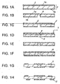
First, as shown in Fig. 1A, metal layers 1a and 1b are adhered to
each side of insulated substrate 2 to form double-side copper-clad
laminate 3. The insulated substrate is made of an insulating material
selected from epoxy resin impregnated glass-cloth substrate , epoxy
resin impregnated aramid-unwoven cloth substrate, polyimide resin
impregnated glass-cloth substrate, polyimide resin impregnated
aramid-unwoven cloth substrate, bismaleimide-triazine resin laminate,
and the like.
Copper foils can be used as metal layers 1a and 1b adhered to
both sides of insulated substrate 2. Preferably, copper foils are treated
to have roughened surfaces to improve adhesive properties thereof.
Alternatively, metal layers 1a and 1b can be copper deposit
formed on the surfaces of insulated substrate 2 by electroless copper
plating followed by electrolytic copper plating.
Preferably, the thickness of insulated substrate 2 ranges 50 to
100µm. With a thickness less than 50µm, the substrate is too weak to
be handled and mass-produced. With a thickness exceeding 100µm, it
is difficult to form micro-via-hole-forming openings and such a
substrate hardly suits to electronic equipment where lightness and
thinness are required.
As for metal layers 1a and 1b, it is preferable that the thickness
of metal layer 1b on the side to be drilled ranges 3 to 18µm and the
thickness of metal layer 1a on the side not to be drilled ranges 5 to
18µm.
When via-hole-forming openings are formed in the insulated
substrate by laser machining, the drilling operation is easier with
thinner metal layer 1b on the side to be drilled. However, with a
thickness less than 3µm, problems in electrical and mechanical
properties hinder formation of metal layers suitable for mass-production.
With a thickness exceeding 18µm, formation of fine
patterns by etching is difficult. When the thickness of metal layer 1a
on the side not to be drilled is less than 5µm, the metal layer may be
penetrated through.
Preferably, a double-side copper-clad laminate of glass-cloth-substrate
epoxy resin is used as insulated substrate 2 and metal layers
1a and 1b. The double-side copper-clad laminate is obtained by
interposing a sheet of B-staged prepreg made of a glass cloth
impregnated with epoxy resin between copper foils and hot-pressing
these materials.
Next, as shown in Fig. 1B, laser radiation is performed in a
desired position on one side of double-side copper-clad laminate 3 to
form via-hole-forming opening 4 that penetrates through metal layer 1b
and insulated substrate 2 and extends to the other metal layer 1a.
There are three methods of drilling via-hole-forming opening 4.
A first method is irradiating the side of metal layer 1b on
insulated substrate 2 with UV-YAG laser, to form via-hole-forming
opening 4.
A second method is irradiating metal layer 1b on insulated
substrate 2 with YAG laser to drill a hole, and thereafter irradiating
insulated substrate 2 with carbon dioxide gas laser, to form via-hole-forming
opening 4.
A third method is irradiating the side of metal layer 1b on
insulated substrate 2 with carbon dioxide gas laser and drilling metal
layer 1b and the insulated substrate layer, while controlling the energy
of the laser, to form via-hole-forming opening 4.
In the third method, it is important that the carbon dioxide gas
laser pulse energy to metal layer 1b is at least 19mJ and that to
insulated substrate 2 is 0.5 to 5mJ. When metal layer 1b is drilled
with a laser pulse energy less than 19 mJ, burrs are generated and
obtaining smooth drilled surfaces is difficult. As for insulated
substrate 2, it is difficult to drill with a laser pulse energy less than 0.5
mJ. With a laser pulse energy exceeding 5 mJ, the drilled surface is
rough, the cut surface of the glass cloth has glass-bead-like slug, or
metal layer 1a at the bottom of the via hole tends to severely be
damaged.
In addition, it is preferable that the diameter of via-hole-forming
opening 4 formed in double-side copper-clad laminate 3 of this
embodiment ranges 30 to 250 µm. With a diameter of the opening less
than 30 µm, the opening is difficult to be filled with electro-conductive
material, and moreover, connection reliability decreases. With a
diameter of the opening exceeding 250 µm, it is difficult to fill the
opening with electro-conductive material completely.
In order to ensure connection reliability, it is preferable to
subsequently perform desmear treatment, e.g. chemical treatment,
oxygen plasma treatment, corona discharge, for removing resin
remaining on the inner wall of via-hole-forming opening 4.
Next, as shown in Fig. 1C, plating-resistant tape 6 is adhered to
the surface of metal layer 1a on double-side copper-clad laminate 3 that
has no via-hole-forming opening 4 formed therethrough, except for
power supply portion 5 for electrolytic plating. This plating-resistant
tape 6 is used to inhibit metallic deposit formed on metal layer 1a in
electrolytic plating process, which is described later. Such tapes
include a polyethylene terephthalate (PET) film having an adhesive
layer formed on the surface thereof.
Subsequently, as shown in Fig. 1D, via post 8 is deposited by
electrolytic plating process, using power supply portion for electrolytic
plating 5 of metal layer 1a as plating lead 7, and thereby via hole
conductor 9 is formed.
Metals used for electrolytic plating include copper, gold, nickel,
and solder. It is preferable to use electrolytic copper plating.
The electrolytic plating process of this embodiment is performed
using metal layer 1a as plating lead 7. Since metal layer 1a is formed
over the entire surface of one side of double-side copper-clad laminate 3,
the density of the electric field is substantially uniform. This allows
the formation of electrolytic metallic deposit of a substantially equal
height in each via-hole-forming opening 4. Moreover, since no power is
supplied to metal layer 1b on double-side copper-clad laminate 3, metal
does not build up on metal layer 1b and the copper foil can keep the
original thickness thereof.
Once filling via-hole-forming opening 4 with metal deposit, the
metallic deposit electrically connects to metal layer 1b on double-side
copper-clad laminate 3 and thus metallic deposit develops on the
surface of metal layer 1b. Because the plated area extends over the
entire surface of metal layer 1b, the density of current that has been
applied only to via-hole-forming opening 4 drastically decreases, and
thus the speed of metallic deposition considerably reduces. As a result,
each via post has substantially an equal height.
Next, as shown in Figs. 1E to 1G, plating-resistant tape 6
adhered to metal layer 1a is delaminated, etching resists 10 are
adhered onto metal layers 1a and 1 on double-side copper-clad
laminate 3, and metal layers 1a and 1b are etched via masks having
predetermined patterns. Thus, circuits 11 are formed.
In this etching process, first, photosensitive dry film resists are
adhered onto respective surfaces of metal layers 1a and 1b or liquid
photo resist is applied thereto. Subsequently, the resists are exposed
to light and developed according to the predetermined circuit patterns,
and thus etching resist patterns are formed. Then, part of metal
layers 1a and 1b where no etching resist patterns have formed is etched
and circuits 11 are provided.
Preferably used chemical solutions for etching is at least one
kind selected from solutions of ferric chloride, cupric chloride,
pursulfate, and sulfuric acid-hydrogen peroxide.
After delamination of etching resists 10, the surfaces of circuits
11 are roughened to form roughened surfaces 12, as shown in Fig. 1H.
This roughening process is performed to improve the adhesion
of the circuit boards to a plurality sheets of prepreg for interlayer
connection, which will be described later, and to prevent delamination
in multilayering. The roughening methods include soft etching
treatment, blackening (oxidation and reduction) treatment, and
formation of acicular alloy plating of copper-nickel-phosphorous. After
such a roughening process, Sn-layer or the like is formed over
roughened surface 12 to prevent oxidation.
The via hole formed in the laminating double-side circuit board
of the present invention can be filled with electro-conductive paste.
However, deposit of conductive metal formed by electrolytic plating is
preferable to ensure connection reliability, especially when the
thickness of insulated substrate 2 is less than 100 µm.
Described next is a prepreg for interlayer connection of the
present invention used to bond a plurality of laminating double-side
circuit boards and connect the circuits thereof.
An uncured resin layer usable for the prepreg is made of at least
one kind of heat-resistant organic resin selected from epoxy resins,
polyimide resins, composite resins of epoxy resin and thermoplastic
resin, composite resins of epoxy resin and silicone resin, and BT resin.
When the prepreg is produced by curing a resin to the B stage (semicured
state of resin), the above-mentioned resins may be impregnated
in at least one substrate selected from aramid unwoven cloth, glass
unwoven cloth, glass cloth and the like, and cured to the B stage.
Thereafter, through holes are drilled using carbon dioxide gas
laser and the through holes are filled with electro-conductive material
to provide sheets of prepreg 25 and 33 for interlayer connection as
shown in Fig. 2A.
Preferably, the diameter of the via holes for interlayer connection
made by filling through holes 26 for interlayer connection drilled
through sheets of prepreg 25 and 33 with electro-conductive material
27 ranges 50 to 500 µm. When the diameter of the via holes for
interlayer connection is less than 50 µm, ensuring connection reliability
is difficult. When the diameter exceeds 500 µm, high-density wiring is
difficult.
It is also preferable that electro-conductive material 27 charged
into through holes 26 formed through the sheets of prepreg 25 and 33
for interlayer connection is electro-conductive paste for the following
reason. When the multilayer printed wiring board is pressed and
heated during lamination, the resin in the prepreg, i.e. a substrate
material, shrinks, and thus the electro-conductive paste portion is
compressed. As a result, a multilayer printed wiring board having
excellent connection reliability can be obtained.
Moreover, when electro-conductive paste 27 is formed to protrude
from through holes 26 through the sheets of prepreg 25 and 33, further
connection reliability can be ensured. In other words, after the PET
films are adhered to both sides of the prepreg, the prepreg is drilled
using laser, electro-conductive paste is charged into the through hole,
and the PET films are delaminated, the electro-conductive paste having
the thickness of the PTE film remains in the form of protrusions. By
laminating press, copper particles are tightly charged into the through
hole. As a result, the reliability is improved.
It is preferable to use at least one kind of metal particles selected
from copper, silver, gold, and nickel or the like, as electro-conductive
material in the electro-conductive paste.
The multilayer printed wiring board of the present invention is
structured so that a plurality of laminating double-side circuit boards
of the above-mentioned embodiment and a plurality sheets of prepreg
for interlayer connection (hereinafter referred to simply as "prepreg")
are alternately placed one on another and collectively laminated. The
manufacturing method thereof is described using Figs. 2A and 2B.
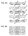
First, as shown in Fig. 2A, laminating double- side circuit boards
21, 30, 36, and two sheets of prepreg 25 and 33 are alternately placed
one on another in the following manner.
Laminating double-side circuit board 21 is placed so that surface
24 having pads formed of a copper foil thereon forms an outermost layer
of the multilayer printed wiring board. Prepreg 25 is positioned so
that pad 23 on the opposite side of the circuit board is opposed to pad 28
on the prepreg, and placed on the circuit board.
Next, laminating double-side circuit board 30 is positioned and
placed so that pad 31 thereon is opposed to pad 29 on prepreg 25. In
addition, prepreg 33 is positioned and placed so that pad 34 thereon is
opposed to pad 32 on laminating double-side circuit board 30.
Next, laminating double-side circuit board 36 is placed so that
surface 38 having pads formed of a copper foil thereon forms another
outermost layer of the multilayer printed wiring board. Prepreg 33
and circuit board 36 are positioned and placed so that pad 37 on the
opposite side of the circuit board is opposed to pad 35 on prepreg 33.
This positioning can be made by inserting guide pins into guide
holes for lamination (not shown) provided around each of the
laminating circuit boards and the sheets of prepreg or by image
processing.
Laminating press is performed on the laminating double-side
circuit boards and the sheets of prepreg laminated in the above-mentioned
manner at a temperature of 180 °C, using a vacuum hot
press. Thus, a multilayer printed wiring board having the IVH
structure throughout layers as shown in Fig. 2B can be obtained.
For each laminating double-side circuit board, the circuits and
via holes thereof can be inspected prior to lamination. This can
drastically improve the yields and reliability of connection between
each layer.
Described next is a specific example of a multilayer printed
wiring board having the IVH structure of the present invention.
After blind via holes are drilled from one side of a double-side
copper-clad glass-clothepoxy resin substrate, using UV-YAG laser, the
insulating-resin substrate is wetted by a solvent and desmear
treatment is performed on the blind via holes, using potassium
permanganate.
Next, plating-resistant tape is laminated on the other side
having no blind via holes formed therethrough, except for the power
supply portion, and power is supplied from the power supply portion for
electrolytic copper plating. Thus, the blind via holes are filled with
copper deposit.
Subsequently, the copper foils are etched via photosensitive dry
film resists. Thereby, wiring patterns are formed and a laminating
double-side circuit board is produced.
Thereafter, using carbon dioxide gas laser, openings are drilled
through an uncured prepreg made of aramid unwoven cloth
impregnated with epoxy resin, and then the openings are filled with
conductive copper paste.
Three laminating double-side circuit boards and two sheets of
prepreg obtained in these manners are alternately placed one on
another. The laminate is pressed at a temperature of 180 °C, using a
vacuum hot press, to provide a multilayer printed wiring board having
the IVH structure throughout layers.
In the electro-conductive copper paste charged in the prepreg,
copper particles are closely bonded and cured by cure and shrinkage of
the prepreg caused by-the press and heat. This close bonding ensures
electrical and mechanical connection between wiring layers.
For a six-layer wiring board produced in this manner, L/S = 50
µm/50 µm, the diameter of each pad is 200 µm, the diameter of each via
hole is 100 µm, the thickness of each conductor layer is 12 µm, and the
thickness of the insulated substrate is 100 µm.
As clearly explained from the embodiments described above, the
laminating double-side circuit board of the present invention is suitable
for production of a multilayer printed wiring board having the IVH
structure throughout layers. In other words, circuits are formed on
both sides of an insulated substrate, via holes are formed through one
side, and the via hole openings are filled with deposit of a conductor.
This structure allows connection of the circuits formed on both sides of
the insulated substrate with high reliability.
The diameter of the via holes provided in a laminating double-side
circuit board of the present invention is smaller than that of the
via holes provided through a prepreg. This structure ensures
connection between each of double-side circuit board layers even when
the laminating double-side circuit boards are slightly displaced with
one another in positioning process during production of a multilayer
printed wiring board.
In electro-conductive paste charged in the prepreg, copper
particles are closely charged by compression caused by cure and
shrinkage of the prepreg. This phenomenon can produce a great effect
in reliability of connection between wiring layers.
Moreover, PET films are laminated on both sides of the prepreg,
holes are drilled using laser and filled with electro-conductive paste,
and the PET films are delaminated. As a result, the electro-conductive
paste protrudes from the surfaces by the thickness of the PET film.
Therefore, copper particles are further closely charged by laminating
press. This process further improves the reliability.
The multilayer printed wiring board of the present invention is
formed so that the via holes under the wiring patterns of the outermost
layers are covered with the copper foils. This structure eliminates
breakage of wire between the via holes and the pads even when the
resin substrate is rapidly expanded or shrunk by thermal shocks or the
like. Thus, the wiring board of the present invention has excellent
connection reliability.
Moreover, the laminating double-side circuit board can be
inspected in the process of production. Therefore, the yield can
drastically be improved and production time of the multilayer printed
wiring board can be reduced. In this manner, this invention has large
industrial value.
Claims (16)
- A laminating double-side circuit board comprising:wherein said circuits on the both sides of said insulated substrate are connected by the electro-conductive material.circuits, each having a pad formed therein, provided on both sides of an insulated substrate; anda via hole extending from one of said circuits on one of the sides of said insulated substrate to an other of said circuits on an other side of the both sides, said via hole filled with electro-conductive material;
- The laminating double-side circuit board as set forth in Claim 1, wherein said circuits having the pads formed therein are formed by etching copper foils on a double-side copper-clad laminate.
- The laminating double-side circuit board as set forth in Claim 1, wherein said insulated substrate is made of glass cloth- epoxy resin substrate 50 to 100 µm in thickness and a diameter of said via hole is 30 to 250 µm.
- A method of manufacturing a laminating double-side circuit board comprising metal layers formed on both sides of an insulated substrate and a via hole extending from one of said metal layers on one of the both sides to an other of said metal layers on an other of the both sides, said method comprising the steps of:irradiating said circuit board with laser light, to form said via hole;thereafter, performing desmear treatment on an inner wall of said via hole; andfilling said via hole with electro-conductive material.
- The method of manufacturing a laminating double-side circuit board as set forth in Claim 4, including the step of:irradiating one of said metal layers formed on the both sides of said insulated substrate with UV-YAG laser, to form said via hole.
- The method of manufacturing a laminating double-side circuit board as set forth in Claim 4 comprising the steps of:irradiating one of said metal layers formed on both sides of said insulated substrate with YAG laser, to drill a hole; andthereafter, irradiating said insulated substrate with carbon dioxide gas laser, to form said via hole.
- The method of manufacturing a laminating double-side circuit board as set forth in Claim 4 comprising the step of:wherein the carbon dioxide gas laser pulse energy to the copper foil is at least 19 mJ and that to the insulated substrate layer ranges 0.5 to 5 mJ.irradiating a copper foil of one of said metal layers formed on the both sides of said insulated substrate and said insulated substrate layer, with carbon dioxide gas laser, while controlling energy of the laser, in order to form said via hole,
- The method of manufacturing a laminating double-side circuit board as set forth in Claim 4 comprising the steps of:performing desmear treatment on an inner wall of said via hole formed by said laser, after said laser radiation step;thereafter, adhering a resin film to a surface having no via hole formed therethrough, said surface being one of said metal layers formed on the both sides of said insulated substrate; andfilling said via hole with the electro-conductive material, to form a via hole for connection; andthereafter, forming a circuit pattern by etching.
- The method of manufacturing a laminating double-side circuit board as set forth in Claim 4, wherein the electro-conductive material is made of copper deposit formed by the steps of:adhering a plating-resistant tape to a surface having no via hole formed therethrough, said surface being one of said metal layers formed on the both sides of said insulated substrate; andsupplying power to said surface for electrolytic copper plating.
- The method of manufacturing a laminating double-side circuit board as set forth in Claim 4, wherein a metal surface of said circuit having a pad formed therein, provided on said insulated substrate is roughened, and an anti-oxidant layer is formed on the roughened surface.
- A multilayer printed wiring board comprising a plurality of laminating double-side circuit boards and a plurality sheets of prepreg for interlayer connection alternately placed one on another, said wiring board comprising:whrein the respective pads are opposed via a through hole filled with electro-conductive material formed through the sheet of prepreg, and thereby the respective pads on said plurality of laminating double-side circuit boards are electrically connected with one another, and said multilayer printed wiring board is structured so that said plurality of laminating double-side circuit boards and said plurality sheets of prepreg for interlayer connection are laminated.a pad on one of said laminating double-side circuit boards; andanother pad on another one of said laminating double-side circuit boards to be connected via one of said sheets of prepreg for interlayer connection,
- The multilayer printed wiring board as set forth in Claim 11, wherein both outermost layers of said multilayer printed wiring board are made of surfaces of said laminating double-side circuit boards having the pads made of metal layers.
- The multilayer printed wiring board as set forth in Claim 11, wherein each sheet of prepreg for interlayer connection has an uncured resin layer and said through hole, and said through hole is filled with the electro-conductive material.
- The multilayer printed wiring board as set forth in Claim 11, wherein each sheet of prepreg for interlayer connection has an uncured resin layer and at least one of an unwoven cloth and a fiber.
- The multilayer printed wiring board as set forth in Claim 11, wherein said through hole provided through each of sheets of prepreg for interlayer connection has a diameter larger than that of a via hole in each of said laminating double-side circuit boards, and the diameter of said through hole ranges 50 to 500 µm.
- The multilayer printed wiring board as set forth in Claim 11, wherein each of said sheets of prepreg for interlayer connection is made by drilling said through hole, using carbon dioxide gas laser, through an uncured prepreg of aramid unwoven cloth impregnated with epoxy resin, and by filling said through hole with the electro-conductive material.
Applications Claiming Priority (3)
| Application Number | Priority Date | Filing Date | Title |
|---|---|---|---|
| JP2001021152 | 2001-01-30 | ||
| JP2001021152A JP2002232135A (en) | 2001-01-30 | 2001-01-30 | Double-sided circuit board for lamination, method for manufacturing the same, and multilayer printed wiring board using the same |
| PCT/JP2002/000639 WO2002062116A1 (en) | 2001-01-30 | 2002-01-29 | It laminating double-side circuit board and production method therefor and multi-layer printed circuit board using |
Publications (2)
| Publication Number | Publication Date |
|---|---|
| EP1283662A1 true EP1283662A1 (en) | 2003-02-12 |
| EP1283662A4 EP1283662A4 (en) | 2007-01-10 |
Family
ID=18886754
Family Applications (1)
| Application Number | Title | Priority Date | Filing Date |
|---|---|---|---|
| EP02710365A Withdrawn EP1283662A4 (en) | 2001-01-30 | 2002-01-29 | IT LAMINATE DOUBLE-SIDED PCB AND MANUFACTURING METHOD USING THEREOF AND MULTILAYER CONDUCTOR PLATE |
Country Status (5)
| Country | Link |
|---|---|
| US (1) | US7151228B2 (en) |
| EP (1) | EP1283662A4 (en) |
| JP (1) | JP2002232135A (en) |
| CN (1) | CN1282404C (en) |
| WO (1) | WO2002062116A1 (en) |
Cited By (4)
| Publication number | Priority date | Publication date | Assignee | Title |
|---|---|---|---|---|
| EP1450590A3 (en) * | 2003-02-24 | 2007-01-17 | Endicott Interconnect Technologies, Inc. | Circuitized substrate and method of making same |
| EP1811824A4 (en) * | 2005-11-07 | 2007-12-12 | Matsushita Electric Industrial Co Ltd | Multilayer printed wiring board and process for producing the same |
| EP2416632A1 (en) * | 2010-04-20 | 2012-02-08 | Subtron Technology Co., Ltd. | Circuit substrate and manufacturing method thereof |
| US8906627B2 (en) | 2002-09-24 | 2014-12-09 | Duke University | Apparatuses and methods for manipulating droplets |
Families Citing this family (51)
| Publication number | Priority date | Publication date | Assignee | Title |
|---|---|---|---|---|
| JP2003046249A (en) * | 2001-08-02 | 2003-02-14 | Ibiden Co Ltd | Lamination wiring board and its manufacturing method |
| US6852627B2 (en) * | 2003-03-05 | 2005-02-08 | Micron Technology, Inc. | Conductive through wafer vias |
| JP4054269B2 (en) | 2003-03-20 | 2008-02-27 | Tdk株式会社 | Electronic component manufacturing method and electronic component |
| JP2005045150A (en) * | 2003-07-25 | 2005-02-17 | Matsushita Electric Ind Co Ltd | Wiring substrate for intermediate connection, multilayer wiring board, and manufacturing method thereof |
| JP4131694B2 (en) | 2003-10-06 | 2008-08-13 | 三洋電機株式会社 | Multilayer ceramic substrate and manufacturing method thereof |
| JP2006019636A (en) * | 2004-07-05 | 2006-01-19 | Renesas Technology Corp | Semiconductor device |
| US7426780B2 (en) * | 2004-11-10 | 2008-09-23 | Enpirion, Inc. | Method of manufacturing a power module |
| US7344915B2 (en) * | 2005-03-14 | 2008-03-18 | Advanced Semiconductor Engineering, Inc. | Method for manufacturing a semiconductor package with a laminated chip cavity |
| JP4534062B2 (en) | 2005-04-19 | 2010-09-01 | ルネサスエレクトロニクス株式会社 | Semiconductor device |
| JP2006324568A (en) * | 2005-05-20 | 2006-11-30 | Matsushita Electric Ind Co Ltd | Multilayer module and manufacturing method thereof |
| JP4659549B2 (en) * | 2005-07-27 | 2011-03-30 | 富士通株式会社 | Design information generation program, design information generation apparatus, and design information generation method |
| US8701272B2 (en) | 2005-10-05 | 2014-04-22 | Enpirion, Inc. | Method of forming a power module with a magnetic device having a conductive clip |
| US7688172B2 (en) | 2005-10-05 | 2010-03-30 | Enpirion, Inc. | Magnetic device having a conductive clip |
| US8631560B2 (en) | 2005-10-05 | 2014-01-21 | Enpirion, Inc. | Method of forming a magnetic device having a conductive clip |
| JP4287458B2 (en) * | 2005-11-16 | 2009-07-01 | サムソン エレクトロ−メカニックス カンパニーリミテッド. | Printed circuit board using paste bump and manufacturing method thereof |
| US7920042B2 (en) | 2007-09-10 | 2011-04-05 | Enpirion, Inc. | Micromagnetic device and method of forming the same |
| JP5436774B2 (en) * | 2007-12-25 | 2014-03-05 | 古河電気工業株式会社 | Multilayer printed circuit board and manufacturing method thereof |
| US9054086B2 (en) | 2008-10-02 | 2015-06-09 | Enpirion, Inc. | Module having a stacked passive element and method of forming the same |
| US8266793B2 (en) * | 2008-10-02 | 2012-09-18 | Enpirion, Inc. | Module having a stacked magnetic device and semiconductor device and method of forming the same |
| US8339802B2 (en) | 2008-10-02 | 2012-12-25 | Enpirion, Inc. | Module having a stacked magnetic device and semiconductor device and method of forming the same |
| CN102405692A (en) * | 2009-04-02 | 2012-04-04 | 松下电器产业株式会社 | Circuit substrate control method and circuit substrate |
| JP4768059B2 (en) * | 2009-08-12 | 2011-09-07 | タツタ電線株式会社 | Multilayer flexible printed wiring board |
| TW201110839A (en) * | 2009-09-04 | 2011-03-16 | Advanced Semiconductor Eng | Substrate structure and method for manufacturing the same |
| US8567053B2 (en) * | 2010-06-03 | 2013-10-29 | Ddi Global Corp. | Methods of manufacturing printed circuit boards |
| CN103781292B (en) * | 2012-10-17 | 2017-09-19 | 碁鼎科技秦皇岛有限公司 | Circuit board and preparation method thereof |
| JP2014216552A (en) * | 2013-04-26 | 2014-11-17 | 富士通株式会社 | Laminate structure and process of manufacturing the same |
| CN103744226B (en) * | 2013-12-30 | 2017-11-03 | 深圳市华星光电技术有限公司 | Touch control display apparatus |
| US9620841B2 (en) * | 2014-06-13 | 2017-04-11 | Nxp Usa, Inc. | Radio frequency coupling structure |
| US10103447B2 (en) | 2014-06-13 | 2018-10-16 | Nxp Usa, Inc. | Integrated circuit package with radio frequency coupling structure |
| US9887449B2 (en) * | 2014-08-29 | 2018-02-06 | Nxp Usa, Inc. | Radio frequency coupling structure and a method of manufacturing thereof |
| US10225925B2 (en) * | 2014-08-29 | 2019-03-05 | Nxp Usa, Inc. | Radio frequency coupling and transition structure |
| KR101673176B1 (en) * | 2015-08-06 | 2016-11-07 | 주식회사 써키트 플렉스 | Manufacturing method for LED package type FPCB using FCCL or Copper plate, and LED package produced thereby |
| TWI559465B (en) * | 2015-08-14 | 2016-11-21 | 恆勁科技股份有限公司 | Package substrate and manufacturing method thereof |
| CN106658960A (en) * | 2015-10-29 | 2017-05-10 | 富葵精密组件(深圳)有限公司 | Flexible circuit board and manufacturing method thereof |
| CN107404804B (en) * | 2016-05-20 | 2020-05-22 | 鹏鼎控股(深圳)股份有限公司 | Circuit board and method of making the same |
| US10801137B2 (en) | 2016-07-21 | 2020-10-13 | International Business Machines Corporation | Glass cloth including attached fibers |
| CN107155266B (en) * | 2017-06-20 | 2020-10-23 | 广州兴森快捷电路科技有限公司 | Z-direction interconnection circuit board and manufacturing method thereof |
| CN109219329B (en) * | 2017-06-30 | 2021-02-09 | 庆鼎精密电子(淮安)有限公司 | Method for manufacturing circuit board |
| JP7062331B2 (en) * | 2017-11-16 | 2022-05-06 | 株式会社ディスコ | Manufacturing method of core material and manufacturing method of copper-clad laminate |
| US20190335593A1 (en) * | 2018-04-26 | 2019-10-31 | Daeduck Electronics Co., Ltd. | Method of manufacturing the printed circuit board |
| US10172244B1 (en) * | 2018-05-09 | 2019-01-01 | International Business Machines Corporation | Construction of printed circuit board having a buried via |
| CN111385963A (en) * | 2018-12-29 | 2020-07-07 | 深南电路股份有限公司 | Multilayer circuit board and preparation method thereof |
| JP7125547B2 (en) * | 2018-12-29 | 2022-08-24 | 深南電路股▲ふん▼有限公司 | Printed circuit board that can be assembled in various ways and its manufacturing method |
| US11576265B2 (en) * | 2019-01-01 | 2023-02-07 | Ofuna Enterprise Japan Co., Ltd. | Manufacturing method for printed circuit board and laser processing machine |
| CN112312650A (en) * | 2019-08-02 | 2021-02-02 | 李家铭 | Fine interlayer circuit structure and its manufacturing method |
| CN112582386B (en) * | 2019-09-27 | 2022-05-27 | 珠海格力电器股份有限公司 | Power module, preparation method thereof and electrical equipment |
| CN113099610A (en) * | 2019-12-23 | 2021-07-09 | 深圳市亚达明科技有限公司 | Double-sided flexible circuit board mounting manufacturing method |
| US12489044B2 (en) * | 2021-01-26 | 2025-12-02 | Toyobo Co., Ltd. | Method for producing layered body, layered body, and multilayered body |
| JP7448828B2 (en) * | 2021-09-30 | 2024-03-13 | 日亜化学工業株式会社 | Wiring board, light emitting device and manufacturing method thereof |
| TWI810728B (en) * | 2021-11-29 | 2023-08-01 | 貿聯國際股份有限公司 | Circuit board |
| CN116456632B (en) * | 2023-06-15 | 2023-08-25 | 广州添利电子科技有限公司 | Pressing manufacturing method of high-rise PCB |
Family Cites Families (19)
| Publication number | Priority date | Publication date | Assignee | Title |
|---|---|---|---|---|
| US4591411A (en) * | 1982-05-05 | 1986-05-27 | Hughes Aircraft Company | Method for forming a high density printed wiring board |
| US4964948A (en) * | 1985-04-16 | 1990-10-23 | Protocad, Inc. | Printed circuit board through hole technique |
| US4967314A (en) * | 1988-03-28 | 1990-10-30 | Prime Computer Inc. | Circuit board construction |
| EP0645950B1 (en) * | 1993-09-21 | 1998-09-02 | Matsushita Electric Industrial Co., Ltd. | Connecting member of a circuit substrate and method of manufacturing multilayer circuit substrates by using the same |
| US5601672A (en) * | 1994-11-01 | 1997-02-11 | International Business Machines Corporation | Method for making ceramic substrates from thin and thick ceramic greensheets |
| JP3197213B2 (en) * | 1996-05-29 | 2001-08-13 | 松下電器産業株式会社 | Printed wiring board and method of manufacturing the same |
| DE19719700A1 (en) * | 1997-05-09 | 1998-11-12 | Siemens Ag | Blind hole production in circuit board |
| JP3961092B2 (en) * | 1997-06-03 | 2007-08-15 | 株式会社東芝 | Composite wiring board, flexible substrate, semiconductor device, and method of manufacturing composite wiring board |
| JP3359550B2 (en) * | 1997-10-08 | 2002-12-24 | イビデン株式会社 | Multilayer printed wiring board and method of manufacturing the same |
| FI982568A7 (en) * | 1997-12-02 | 1999-06-03 | Samsung Electro Mech | Method for manufacturing a multilayer printed circuit board |
| US6280641B1 (en) | 1998-06-02 | 2001-08-28 | Mitsubishi Gas Chemical Company, Inc. | Printed wiring board having highly reliably via hole and process for forming via hole |
| JP3431523B2 (en) * | 1998-12-09 | 2003-07-28 | 松下電器産業株式会社 | Circuit board connecting material, method of manufacturing the same, and method of manufacturing multilayer circuit board using circuit board connecting material |
| JP2000188471A (en) | 1998-12-22 | 2000-07-04 | Ibiden Co Ltd | Printed wiring board and its manufacture |
| US6039889A (en) * | 1999-01-12 | 2000-03-21 | Fujitsu Limited | Process flows for formation of fine structure layer pairs on flexible films |
| JP2000232269A (en) * | 1999-02-10 | 2000-08-22 | Nec Toyama Ltd | Printed wiring board and manufacture thereof |
| JP3702698B2 (en) | 1999-03-16 | 2005-10-05 | 松下電器産業株式会社 | High frequency module |
| JP2000269647A (en) * | 1999-03-18 | 2000-09-29 | Ibiden Co Ltd | Single-sided circuit board, multilayer printed wiring board and method of manufacturing the same |
| JP2000286549A (en) | 1999-03-24 | 2000-10-13 | Fujitsu Ltd | Method for manufacturing substrate with via connection |
| US6329603B1 (en) * | 1999-04-07 | 2001-12-11 | International Business Machines Corporation | Low CTE power and ground planes |
-
2001
- 2001-01-30 JP JP2001021152A patent/JP2002232135A/en active Pending
-
2002
- 2002-01-29 WO PCT/JP2002/000639 patent/WO2002062116A1/en not_active Ceased
- 2002-01-29 US US10/203,971 patent/US7151228B2/en not_active Expired - Fee Related
- 2002-01-29 EP EP02710365A patent/EP1283662A4/en not_active Withdrawn
- 2002-01-29 CN CN02800056.0A patent/CN1282404C/en not_active Expired - Fee Related
Cited By (6)
| Publication number | Priority date | Publication date | Assignee | Title |
|---|---|---|---|---|
| US8906627B2 (en) | 2002-09-24 | 2014-12-09 | Duke University | Apparatuses and methods for manipulating droplets |
| US9110017B2 (en) | 2002-09-24 | 2015-08-18 | Duke University | Apparatuses and methods for manipulating droplets |
| US9638662B2 (en) | 2002-09-24 | 2017-05-02 | Duke University | Apparatuses and methods for manipulating droplets |
| EP1450590A3 (en) * | 2003-02-24 | 2007-01-17 | Endicott Interconnect Technologies, Inc. | Circuitized substrate and method of making same |
| EP1811824A4 (en) * | 2005-11-07 | 2007-12-12 | Matsushita Electric Industrial Co Ltd | Multilayer printed wiring board and process for producing the same |
| EP2416632A1 (en) * | 2010-04-20 | 2012-02-08 | Subtron Technology Co., Ltd. | Circuit substrate and manufacturing method thereof |
Also Published As
| Publication number | Publication date |
|---|---|
| WO2002062116A1 (en) | 2002-08-08 |
| JP2002232135A (en) | 2002-08-16 |
| EP1283662A4 (en) | 2007-01-10 |
| US20040104042A1 (en) | 2004-06-03 |
| US7151228B2 (en) | 2006-12-19 |
| CN1282404C (en) | 2006-10-25 |
| CN1456030A (en) | 2003-11-12 |
Similar Documents
| Publication | Publication Date | Title |
|---|---|---|
| US7151228B2 (en) | Laminating double-side circuit board, manufacturing method thereof, and multilayer printed circuit board using same | |
| EP1009205B1 (en) | Single-sided circuit board and method for manufacturing the same | |
| US6440542B1 (en) | Copper-clad laminated board, and circuit board for printed wiring board and method for producing the same | |
| WO2001045478A1 (en) | Multilayered printed wiring board and production method therefor | |
| WO1997048260A1 (en) | One-sided circuit board for multi-layer printed wiring board, multi-layer printed wiring board, and method for its production | |
| JP4043115B2 (en) | Multi-layer printed wiring board | |
| JPH1154934A (en) | Multilayered printed wiring board and its manufacture | |
| KR100349119B1 (en) | A printed circuit board and method of fabricating thereof | |
| JP3492467B2 (en) | Single-sided circuit board for multilayer printed wiring board, multilayer printed wiring board and method of manufacturing the same | |
| JPH1154926A (en) | One-sided circuit board and its manufacture | |
| JP2000269647A (en) | Single-sided circuit board, multilayer printed wiring board and method of manufacturing the same | |
| JP2001015919A (en) | Multilayer printed wiring board, circuit-board therefor and its manufacture | |
| JPH1041635A (en) | Single-sided circuit board for multilayer printed wiring board, its manufacture, and multilayer printed wiring board | |
| JP3253886B2 (en) | Single-sided circuit board for multilayer printed wiring board, method for manufacturing the same, and multilayer printed wiring board | |
| JP4545865B2 (en) | Method for manufacturing circuit board for multilayer printed wiring board | |
| JP2002198652A (en) | Multilayer printed wiring board, method of manufacturing the same and single-sided circuit board therefor | |
| JP3492667B2 (en) | Single-sided circuit board for multilayer printed wiring board, multilayer printed wiring board and method of manufacturing the same | |
| JP3540809B2 (en) | Single-sided circuit board for high density multilayer printed wiring board and high density multilayer printed wiring board | |
| KR20040065861A (en) | Printed circuit board for using all layer interstitial via hole, and manufacturing method thereof | |
| JPH11126968A (en) | Manufacture of multilayered printed wiring board | |
| JP2004363325A (en) | Multilayer wiring board and method of manufacturing the same | |
| JPH11186726A (en) | Multilayered printed wiring board and manufacture thereof | |
| JP2000183528A (en) | Manufacture of multilayer printed wiring board | |
| JPH06296083A (en) | Manufacture of wiring board | |
| JPH1051139A (en) | Single-sided circuit board for multilayer printed-wiring board and its manufacture as well as multilayer printed-wiring board |
Legal Events
| Date | Code | Title | Description |
|---|---|---|---|
| PUAI | Public reference made under article 153(3) epc to a published international application that has entered the european phase |
Free format text: ORIGINAL CODE: 0009012 |
|
| 17P | Request for examination filed |
Effective date: 20020927 |
|
| AK | Designated contracting states |
Designated state(s): AT BE CH CY DE DK ES FI FR GB GR IE IT LI LU MC NL PT SE TR |
|
| A4 | Supplementary search report drawn up and despatched |
Effective date: 20061208 |
|
| 17Q | First examination report despatched |
Effective date: 20080804 |
|
| RAP1 | Party data changed (applicant data changed or rights of an application transferred) |
Owner name: PANASONIC CORPORATION |
|
| STAA | Information on the status of an ep patent application or granted ep patent |
Free format text: STATUS: THE APPLICATION IS DEEMED TO BE WITHDRAWN |
|
| 18D | Application deemed to be withdrawn |
Effective date: 20150801 |