EP1278239A1 - Verfahren zur Herstellung selbstjustierender Maskenschichten - Google Patents
Verfahren zur Herstellung selbstjustierender Maskenschichten Download PDFInfo
- Publication number
- EP1278239A1 EP1278239A1 EP01117545A EP01117545A EP1278239A1 EP 1278239 A1 EP1278239 A1 EP 1278239A1 EP 01117545 A EP01117545 A EP 01117545A EP 01117545 A EP01117545 A EP 01117545A EP 1278239 A1 EP1278239 A1 EP 1278239A1
- Authority
- EP
- European Patent Office
- Prior art keywords
- insulation layer
- curvature
- etching
- trench
- layer
- Prior art date
- Legal status (The legal status is an assumption and is not a legal conclusion. Google has not performed a legal analysis and makes no representation as to the accuracy of the status listed.)
- Granted
Links
Images





Classifications
-
- H—ELECTRICITY
- H10—SEMICONDUCTOR DEVICES; ELECTRIC SOLID-STATE DEVICES NOT OTHERWISE PROVIDED FOR
- H10P—GENERIC PROCESSES OR APPARATUS FOR THE MANUFACTURE OR TREATMENT OF DEVICES COVERED BY CLASS H10
- H10P14/00—Formation of materials, e.g. in the shape of layers or pillars
- H10P14/60—Formation of materials, e.g. in the shape of layers or pillars of insulating materials
- H10P14/69—Inorganic materials
- H10P14/692—Inorganic materials composed of oxides, glassy oxides or oxide-based glasses
- H10P14/6921—Inorganic materials composed of oxides, glassy oxides or oxide-based glasses containing silicon
- H10P14/6922—Inorganic materials composed of oxides, glassy oxides or oxide-based glasses containing silicon the material containing Si, O and at least one of H, N, C, F or other non-metal elements, e.g. SiOC, SiOC:H or SiONC
- H10P14/6923—Inorganic materials composed of oxides, glassy oxides or oxide-based glasses containing silicon the material containing Si, O and at least one of H, N, C, F or other non-metal elements, e.g. SiOC, SiOC:H or SiONC the material being boron or phosphorus doped silicon oxides, e.g. BPSG, BSG or PSG
-
- H—ELECTRICITY
- H10—SEMICONDUCTOR DEVICES; ELECTRIC SOLID-STATE DEVICES NOT OTHERWISE PROVIDED FOR
- H10B—ELECTRONIC MEMORY DEVICES
- H10B12/00—Dynamic random access memory [DRAM] devices
- H10B12/01—Manufacture or treatment
- H10B12/02—Manufacture or treatment for one transistor one-capacitor [1T-1C] memory cells
- H10B12/03—Making the capacitor or connections thereto
- H10B12/038—Making the capacitor or connections thereto the capacitor being in a trench in the substrate
- H10B12/0385—Making a connection between the transistor and the capacitor, e.g. buried strap
-
- H—ELECTRICITY
- H10—SEMICONDUCTOR DEVICES; ELECTRIC SOLID-STATE DEVICES NOT OTHERWISE PROVIDED FOR
- H10B—ELECTRONIC MEMORY DEVICES
- H10B12/00—Dynamic random access memory [DRAM] devices
- H10B12/01—Manufacture or treatment
- H10B12/02—Manufacture or treatment for one transistor one-capacitor [1T-1C] memory cells
- H10B12/03—Making the capacitor or connections thereto
- H10B12/038—Making the capacitor or connections thereto the capacitor being in a trench in the substrate
- H10B12/0387—Making the trench
-
- H—ELECTRICITY
- H10—SEMICONDUCTOR DEVICES; ELECTRIC SOLID-STATE DEVICES NOT OTHERWISE PROVIDED FOR
- H10P—GENERIC PROCESSES OR APPARATUS FOR THE MANUFACTURE OR TREATMENT OF DEVICES COVERED BY CLASS H10
- H10P14/00—Formation of materials, e.g. in the shape of layers or pillars
- H10P14/60—Formation of materials, e.g. in the shape of layers or pillars of insulating materials
- H10P14/63—Formation of materials, e.g. in the shape of layers or pillars of insulating materials characterised by the formation processes
- H10P14/6326—Deposition processes
- H10P14/6328—Deposition from the gas or vapour phase
- H10P14/6334—Deposition from the gas or vapour phase using decomposition or reaction of gaseous or vapour phase compounds, i.e. chemical vapour deposition
-
- H—ELECTRICITY
- H10—SEMICONDUCTOR DEVICES; ELECTRIC SOLID-STATE DEVICES NOT OTHERWISE PROVIDED FOR
- H10P—GENERIC PROCESSES OR APPARATUS FOR THE MANUFACTURE OR TREATMENT OF DEVICES COVERED BY CLASS H10
- H10P14/00—Formation of materials, e.g. in the shape of layers or pillars
- H10P14/60—Formation of materials, e.g. in the shape of layers or pillars of insulating materials
- H10P14/63—Formation of materials, e.g. in the shape of layers or pillars of insulating materials characterised by the formation processes
- H10P14/6326—Deposition processes
- H10P14/6342—Liquid deposition, e.g. spin-coating, sol-gel techniques or spray coating
-
- H—ELECTRICITY
- H10—SEMICONDUCTOR DEVICES; ELECTRIC SOLID-STATE DEVICES NOT OTHERWISE PROVIDED FOR
- H10P—GENERIC PROCESSES OR APPARATUS FOR THE MANUFACTURE OR TREATMENT OF DEVICES COVERED BY CLASS H10
- H10P14/00—Formation of materials, e.g. in the shape of layers or pillars
- H10P14/60—Formation of materials, e.g. in the shape of layers or pillars of insulating materials
- H10P14/66—Formation of materials, e.g. in the shape of layers or pillars of insulating materials characterised by the type of materials
- H10P14/668—Formation of materials, e.g. in the shape of layers or pillars of insulating materials characterised by the type of materials the materials being characterised by the deposition precursor materials
- H10P14/6681—Formation of materials, e.g. in the shape of layers or pillars of insulating materials characterised by the type of materials the materials being characterised by the deposition precursor materials the precursor containing a compound comprising Si
- H10P14/6684—Formation of materials, e.g. in the shape of layers or pillars of insulating materials characterised by the type of materials the materials being characterised by the deposition precursor materials the precursor containing a compound comprising Si the compound comprising silicon and oxygen
- H10P14/6686—Formation of materials, e.g. in the shape of layers or pillars of insulating materials characterised by the type of materials the materials being characterised by the deposition precursor materials the precursor containing a compound comprising Si the compound comprising silicon and oxygen the compound being a molecule comprising at least one silicon-oxygen bond and the compound having hydrogen or an organic group attached to the silicon or oxygen, e.g. a siloxane
-
- H—ELECTRICITY
- H10—SEMICONDUCTOR DEVICES; ELECTRIC SOLID-STATE DEVICES NOT OTHERWISE PROVIDED FOR
- H10P—GENERIC PROCESSES OR APPARATUS FOR THE MANUFACTURE OR TREATMENT OF DEVICES COVERED BY CLASS H10
- H10P14/00—Formation of materials, e.g. in the shape of layers or pillars
- H10P14/60—Formation of materials, e.g. in the shape of layers or pillars of insulating materials
- H10P14/69—Inorganic materials
- H10P14/692—Inorganic materials composed of oxides, glassy oxides or oxide-based glasses
- H10P14/6921—Inorganic materials composed of oxides, glassy oxides or oxide-based glasses containing silicon
- H10P14/6922—Inorganic materials composed of oxides, glassy oxides or oxide-based glasses containing silicon the material containing Si, O and at least one of H, N, C, F or other non-metal elements, e.g. SiOC, SiOC:H or SiONC
-
- H—ELECTRICITY
- H10—SEMICONDUCTOR DEVICES; ELECTRIC SOLID-STATE DEVICES NOT OTHERWISE PROVIDED FOR
- H10P—GENERIC PROCESSES OR APPARATUS FOR THE MANUFACTURE OR TREATMENT OF DEVICES COVERED BY CLASS H10
- H10P50/00—Etching of wafers, substrates or parts of devices
- H10P50/69—Etching of wafers, substrates or parts of devices using masks for semiconductor materials
- H10P50/691—Etching of wafers, substrates or parts of devices using masks for semiconductor materials for Group V materials or Group III-V materials
- H10P50/693—Etching of wafers, substrates or parts of devices using masks for semiconductor materials for Group V materials or Group III-V materials characterised by their size, orientation, disposition, behaviour or shape, in horizontal or vertical plane
- H10P50/695—Etching of wafers, substrates or parts of devices using masks for semiconductor materials for Group V materials or Group III-V materials characterised by their size, orientation, disposition, behaviour or shape, in horizontal or vertical plane characterised by the process involved to create the mask, e.g. lift-off masks or sidewalls or to modify the mask
-
- H—ELECTRICITY
- H10—SEMICONDUCTOR DEVICES; ELECTRIC SOLID-STATE DEVICES NOT OTHERWISE PROVIDED FOR
- H10P—GENERIC PROCESSES OR APPARATUS FOR THE MANUFACTURE OR TREATMENT OF DEVICES COVERED BY CLASS H10
- H10P14/00—Formation of materials, e.g. in the shape of layers or pillars
- H10P14/60—Formation of materials, e.g. in the shape of layers or pillars of insulating materials
- H10P14/61—Formation of materials, e.g. in the shape of layers or pillars of insulating materials using masks
Definitions
- the present invention relates to a method for Manufacture of self-adjusting mask layers and in particular to a process for making an undensified conformal mask layer due to a different mechanical stress different etching rates or has a self-adjusting etchback.
- this is based on a method described for the production of a trench capacitor, as found in semiconductor memory cells of semiconductor integrated circuits is used.
- the invention can be found in in the same way generally on microelectronic, micromechanical as well as combinations of microelectronic and micromechanical Systems with such a self-adjusting Etching back can be applied.
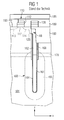
- FIG. 1 shows a conventional trench capacitor, as is used in particular in a DRAM semiconductor memory cell, and is known, for example, from US Pat. No. 5,945,704.
- a DRAM semiconductor memory cell essentially consists of a capacitor 160 which is formed in a substrate 101.
- the substrate 101 is lightly doped with p-type dopants such as boron, for example.
- a trench is usually filled with polysilicon 161, which is heavily n + -doped with, for example, arsenic or phosphorus.
- a buried plate 165 doped with arsenic, for example, is located in the substrate 101 at a lower region of the trench.
- the arsenic or the dopant is usually diffused into the silicon substrate 101 by a dopant source such as, for example, an arsenic silicate glass ASG, which is formed on the side walls of the trench.
- a dopant source such as, for example, an arsenic silicate glass ASG, which is formed on the side walls of the trench.
- the polysilicon 161 and the buried plate 165 serve here as electrodes of the capacitor 160, a dielectric layer 164 separating the electrodes of the capacitor from one another.
- the DRAM semiconductor memory cell according to FIG. 1 has it also a field effect transistor 110.
- This usually transistor designated as a selection transistor a gate 112 and diffusion regions 113 and 114 as source and Drain.
- the diffusion areas separated by a channel 117 are usually spaced by implantation of dopants such as Phosphorus formed.
- An insulation collar 168 is attached to an upper section or upper part of the trench.
- the insulation collar 168 prevents leakage current from the contact diffusion region 125 to buried plate 165.
- One such Leakage current is particularly undesirable in memory circuits, since it is the landing hold time or retention time of a Semiconductor memory cell reduced.
- the conventional semiconductor memory cell with a trench capacitor also a buried trough or Layer 170, where the peak concentration of dopants in the buried n-tub approximately in the lower end of the insulation collar 168 lies.
- the buried trough or layer 170 essentially serves to connect the buried plates 165 of a plurality of adjacent DRAM semiconductor memory cells or capacitors 160 in the carrier substrate 101, which preferably consists of silicon semiconductor material.
- Activation of the selection transistor 110 by applying a suitable voltage to the gate 112 essentially allows access to the trench capacitor 160, usually the gate 112 with a word line 120 and that Diffusion region 113 with a bit line 185 in the DRAM field connected is.
- the bit line 185 is from the diffusion region 113 separated by a dielectric insulation layer 189 and electrically connected via a contact 183.
- isolation of a respective semiconductor memory cell with associated trench capacitor from adjacent Cells a shallow trench isolation (STI, shallow trench isolation) 180 on the surface of the semiconductor substrate 101 trained.
- STI shallow trench isolation
- the word line 120 above the trench and through the flat one Trench isolation (STI) are formed in isolation, which one obtains a so-called folded bit line architecture.
- this insulation collar 168 could also be step-shaped to be hoisted in its other areas only to release the terminal diffusion region 125, wherein however, additional and costly photolithographic Steps and etching steps are to be used. These steps However, they are particularly common in highly integrated circuits Because of so-called overlay problems and "critical dimension" tolerances very complex and costly.
- the invention is therefore based on the object of a method to create self-aligning mask layers, with the microelectronic and micromechanical systems can be produced easily and inexpensively.
- the invention is based on the object Process for producing a self-aligning mask layer to create the insulation collar described above in a particularly simple and inexpensive way is designed such that there is a reduced leakage current and result in improved charge retention properties.
- An undensified layer is preferably used as the conformal insulation layer Oxide and / or glasses based on silicon oxide such as for example, BPSG, PSG and spin-on glasses.
- silicon oxide such as for example, BPSG, PSG and spin-on glasses.
- Such Materials and layers show a strong dependency their internal mechanical stress or their internal stress regarding a surface structure to be masked. By selecting the respective radii of curvature on the surface to be masked, sublithographic Structures realized particularly simply and inexpensively become.
- ozone-TEOS oxide is used as a conformal insulation layer in a CVD process at a pressure of approx. 40 Torr, a temperature of about 400 degrees Celsius and a Separated ozone flow of approx. 4000 sccm, the amount of TEOS is approximately 800 mg / min.
- a conformally deposited Insulation layer has a self-adjusting mask layer extraordinarily favorable dependencies between a respective etching rate and the associated mechanical Stress or an underlying radius of curvature the surface structure.
- the self-adjusting Mask layer or conformal insulation layer compression at, for example, a temperature of 850 to 1000 Degrees Celsius in a nitrogen and / or nitrogen / oxygen atmosphere be carried out, making one for more Process steps an independence of the etching rate of the self-adjusting mask layer depending on the mechanical Stress or the underlying curvature the surface to be masked.
- the once set Structures in the self-aligning mask layer can thus be fixed for later procedural steps.
- An isotropic wet etching which has BHF etching with NH 4 F / HF / H 2 in a ratio of 10/2/90 at room temperature, is preferably carried out as the etch-back of the conformal insulation layer.
- Such an isotropic wet etching shows a particularly high selectivity of the etching rates in the self-adjusting mask layer as a function of the mechanical stress. A period of time and the associated stress on other elements is thus kept to a minimum. Furthermore, it is a standard etching method that is usually available.
- the invention is described below using a DRAM semiconductor memory cell described, for example an insulation collar formed as a self-adjusting mask layer and is structured.
- FIG. 2 shows a simplified sectional view of a semiconductor memory cell with trench capacitor and according to the invention formed insulation collar, the same reference numerals denote the same elements or layers as in Figure 1 and a repeated description is omitted below becomes.
- the insulation collar 168 with one below described manufacturing process, wherein in particular in the connection area AB according to FIG Insulated collar structure (shown in dashed lines) realized becomes.
- the insulation collar 168 accordingly has not a uniform height, but varies in terms of its actual height in a y direction corresponding to that with Dashed lines shown insulation collar structure. According to the invention, the insulation collar 168 is therefore merely in a small area to the contact diffusion area 125 is directed fully open while he is in his further y-directions essentially increases and the contact filler material 162 almost completely encloses, whereby further improved charge retention properties and decreased Leakage currents result.
- FIGS. 3A to 3C show simplified sectional views along an intersection axis I-I ', II-II' and along a surface or x-y plane of a carrier substrate for illustration an early process step according to the present Invention.
- the first step is on a carrier substrate 101, which can represent any material and preferably made of a semiconductor material or silicon there is a mask layer M applied, for example has a photoresist resist.
- this mask layer M a so-called ARC layer (anti reflective coating) with a photoresist or a hard mask with an ARC layer and have a photoresist.
- the mask or the mask layer stack M is made by conventional means lithographic process and possibly necessary Etching processes (for the ARC or hard mask layer) structured. Then the structure of the mask layer M transferred into the carrier substrate 101 by a suitable etching, whereby a surface O to be masked in the carrier substrate 101 is formed. 3A to 3C acts the surface O to be masked is one Trench surface of one formed in the carrier substrate 101 Trench.
- the shape of the surface O to be masked is now essential for the method according to the invention for producing self-adjusting mask layers. More specifically, the surface O to be masked must be formed in the carrier substrate 101 in such a way that different radii of curvature R min to R max result.
- a surface sectional view or sectional view in the xy plane of the trench has an elliptical shape, the vertices A and B of the ellipse having a radius of curvature R max and the vertices C and D having a radius of curvature R min .
- FIGS. 3A and 3B show the associated sectional views along the section lines II 'and II-II' according to FIG. 3C. Alternatively, however, any other structures can be used as surface structures to be masked.
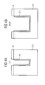
- FIGS. 4A to 4C show simplified sectional views along an intersection axis I-I ', II-II' and a surface or x-y plane to illustrate a further process step, the same reference numerals being the same or corresponding layers or elements as in FIG. 3A to 3C and do not repeat the description becomes.
- an undensified conformal insulation layer SM is now formed on the surface O of the carrier substrate 101 in such a way that regions with different mechanical stresses arise in the insulation layer SM due to the different radii of curvature R min to R max .
- an undensified conformal insulation layer SM with low mechanical stress is formed in an area L based on the radii of curvature, while in the area H, ie the areas with small radii of curvature, the insulation layer SM with high mechanical stress or Stress is trained.
- SM is used as the conformal insulation layer undensified oxide and / or a silicon oxide based Glass such as BPSG (borophosphosilicate glass), PSG (Phosphor silicate glass), spin-on glass, etc., the one such property with respect to the radius of curvature their mechanical stress.
- BPSG borophosphosilicate glass
- PSG Phosphor silicate glass
- spin-on glass etc.
- a CVD process chemical vapor deposition
- an ozone TEOS oxide as a conformal insulation layer SM in a conventional one CVD chamber at a pressure of approximately 40 torr, one Susceptor temperature of, for example, 400 degrees Celsius and an ozone flow of approx. 4000 sccm.
- the amount of TEOS (Tetraethyl orthosilicate) is approx. 800 mg / min.
- etching back step may be necessary, for example, for the self-adjusting Mask layer or the conformal insulation layer SM outside the surface structure to be masked O to remove. So-called lift-off processes are also an alternative applicable.
- the oxide is not yet fully compacted is deposited or healed, otherwise an etch rate selectivity depending on mechanical stress or a mechanical stress in the layer goes.
- the separation can also before removing the mask layer or the mask layer stack M or individual layers thereof.
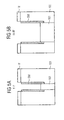
- Figures 5A and 5B show simplified sectional views along an intersection axis I-I 'and II-II' for illustration of such a further method step, the same Identical or corresponding elements or Designate layers as in Figures 3 to 4 and repeat them Description is waived below.
- Figures 6A and 6B show simplified sectional views along an intersection axis I-I 'and II-II' for illustration a self-adjusting etching back step, the same reference numerals again the same or corresponding layers as in Figures 3 to 5 and on a repeated description is subsequently waived.
- FIGS. 6A and 6B there is now a self-adjusting one Etching back to remove parts of the insulation layer or self-adjusting mask layer SM depending of the different mechanical loads in the insulation layer instead.
- Such Etching can be both an adequate wet etching and a dry chemical, possibly plasma-supported etching his. It is essential that the desired etching rate differences depending on the radius of curvature of the masked Structure or the trench surface O by the etching emerge.
- the etching back is preferably carried out wet-chemically as a BHF etching step with NH 4 F / HF / H 2 in a ratio of 10/2/90 at approximately 20 degrees Celsius.
- the etching rate here is approximately 20 nm / minute on bright wafers.
- Adequate selectivity of the etch back due to the different mechanical stresses or the different underlying radii of curvature is obtained if a ratio R max / R min ⁇ 1/8, where R max is the radius of curvature with maximum mechanical stress and R min is the radius of curvature with minimal mechanical stress in the insulation layer or self-adjusting mask layer SM.
- An elliptical shape of the trench in the xy plane is preferably selected, in particular when DRAM semiconductor memory cells are formed.
- the self-adjusting mask layer can densifying the layer can be performed, preferably at a temperature of approx. 850 degrees Celsius to 1000 degrees Celsius in a nitrogen and / or nitrogen / oxygen atmosphere is compressed or healed. Compression is carried out, for example, in an oven process or an RTP process (rapid thermal process). On in this way one obtains that shown in FIGS. 6A and 6B Isolation collar 168, which due to its compression now no or only very slight differences in etching rates depending mechanical stress or the underlying one Has geometry (radius of curvature). Another one Processing can therefore be carried out without changing the structure or respective heights and depths of the insulation collar 168 be performed.
- Figures 7A and 7B show simplified sectional views along an intersection axis I-I 'and II-II' for illustration further method steps, with the same reference numerals same or corresponding elements or layers as in figures Denote 3 to 6 and a repeated description is subsequently waived.
- the trench can now be used with a another electrically conductive filler layer 162 for implementation a connection contact to the contact diffusion region 125 be filled in, with shallow trench isolation (shallow trench isolation, STI) 180 an unintentional contact prevented with the carrier substrate 101.
- shallow trench isolation shallow trench isolation, STI
- Leakage currents can be further reduced which is why a charge holding time is particularly high in semiconductor memory cells is improved.
- the invention has been described above using a DRAM semiconductor memory cell described with an insulation collar. she is however, not limited thereto and includes all others Process for the production of microelectronic and / or micromechanical components in which a self-adjusting mask layer is used.
Landscapes
- Engineering & Computer Science (AREA)
- Manufacturing & Machinery (AREA)
- Semiconductor Memories (AREA)
Abstract
Description
- 101
- Trägersubstrat
- 160
- Grabenkondensator
- 161,
- 162 Füllmaterial
- 164
- dielektrische Schicht
- 165
- vergrabene Platte
- 168
- Isolationskragen
- 170
- vergrabene Wanne
- 180
- flache Grabenisolierung
- 183
- Kontakt
- 185
- Bitleitung
- 189
- Isolierschicht
- 110
- Auswahltransistor
- 112
- Gate
- 113
- Source
- 114
- Drain
- 117
- Kanal
- 120
- Wortleitung
- 125
- Kontakt-Diffusionsgebiet
- AB
- Anschlussbereich
- M
- Maskenschicht (-stapel)
- O
- zu maskierende Oberfläche
- A, B, C, D
- Scheitelpunkte
- Rmin, Rmax
- Krümmungsradien
- SM
- selbstjustierende Maskenschicht
- H, L
- Bereiche mit hoher, geringer mechanischer Beanspruchung
Claims (13)
- Verfahren zur Herstellung einer selbstjustierenden Maskenschicht mit den Schritten:a) Ausbilden einer zu maskierenden Oberfläche (O) in einem Trägersubstrat (101), wobei die Oberfläche (O) unterschiedliche Krümmungsradien (Rmax, Rmin) aufweist;b) Ausbilden einer unverdichteten konformalen Isolationsschicht (SM) auf der Oberfläche (O) derart, dass sich auf Grund der unterschiedlichen Krümmungsradien (Rmin, Rmax) Bereiche (H, L) mit unterschiedlicher mechanischer Beanspruchung in der Isolationsschicht (SM) ergeben;c) Durchführen einer Ätzung zum Entfernen von Teilbereichen der Isolationsschicht (SM) in Abhängigkeit von der unterschiedlichen mechanischen Beanspruchung in der Isolationsschicht (SM).
- Verfahren nach Patentanspruch 1,
dadurch gekennzeichnet, dass in Schritt a) ein Graben im Trägersubstrat (101) ausgebildet wird und die zu maskierende Oberfläche (O) eine Grabenoberfläche darstellt. - Verfahren nach Patentanspruch 1 oder 2,
dadurch gekennzeichnet, dass in Schritt b) als konformale Isolationsschicht (SM) unverdichtete Oxide und/oder auf Siliziumoxid basierte Gläser wie beispielsweise BPSG, PSG und Spin-on-Gläser ausgebildet werden. - Verfahren nach einem der Patentansprüche 1 bis 3,
dadurch gekennzeichnet, dass in Schritt b) ein Ozon-TEOS-Oxid als konformale Isolationsschicht (SM) abgeschieden wird. - Verfahren nach Patentanspruch 4,
dadurch gekennzeichnet, dass das Ozon-TEOS-Oxid mittels eines CVD-Verfahrens bei einem Druck von ca. 40 Torr, einer Temperatur von ca. 400 Grad Celsius und einem Ozonfluss von 4000 sccm abgeschieden wird, wobei die TEOS-Menge ca. 800 mg/min beträgt. - Verfahren nach einem der Patentansprüche 1 bis 5, gekennzeichnet durch den weiteren Schritt d) Verdichten der konformalen Isolationsschicht (SM).
- Verfahren nach Patentanspruch 6,
dadurch gekennzeichnet, dass das Verdichten bei einer Temperatur von ca. 850 Grad Celsius bis 1000 Grad Celsius in einer Stickstoff- und/oder Stickstoff-/Sauerstoffatmosphäre durchgeführt wird. - Verfahren nach Patentanspruch 6 oder 7,
dadurch gekennzeichnet, dass das Verdichten in einem Ofen- oder RTP-Prozess durchgeführt wird. - Verfahren nach einem der Patentansprüche 1 bis 8,
dadurch gekennzeichnet, dass in Schritt c) eine isotrope Nassätzung durchgeführt wird. - Verfahren nach Patentanspruch 9,
dadurch gekennzeichnet, dass in Schritt c) eine BHF-Ätzung mit NH4F/HF/H2 im Verhältnis von 10/2/90 bei ca. 20 Grad Celsius durchgeführt wird. - Verfahren nach einem der Patentansprüche 1 bis 10,
dadurch gekennzeichnet, dass eine Oberflächenschnittansicht der zu maskierenden Oberfläche (O) eine elliptische Form aufweist. - Verfahren nach einem der Patentansprüche 1 bis 11,
dadurch gekennzeichnet, dass ein Verhältnis Rmax/Rmin ≤ 1/8 ist, wobei Rmax der Krümmungsradius mit maximaler und Rmin der Krümmungsradius mit minimaler mechanischer Beanspruchung in der Isolationsschicht (SM) darstellt. - Verfahren nach einem der Patentansprüche 1 bis 12,
dadurch gekennzeichnet, dass es zur Ausbildung eines Kontaktes von einem Grabenkondensator (160) zu einem Auswahltransistor (110) in einer DRAM-Speicherzelle verwendet wird.
Priority Applications (3)
| Application Number | Priority Date | Filing Date | Title |
|---|---|---|---|
| EP01117545A EP1278239B1 (de) | 2001-07-20 | 2001-07-20 | Verfahren zur Herstellung selbstjustierender Maskenschichten |
| DE50107496T DE50107496D1 (de) | 2001-07-20 | 2001-07-20 | Verfahren zur Herstellung selbstjustierender Maskenschichten |
| US10/200,707 US6794259B2 (en) | 2001-07-20 | 2002-07-22 | Method for fabricating self-aligning mask layers |
Applications Claiming Priority (1)
| Application Number | Priority Date | Filing Date | Title |
|---|---|---|---|
| EP01117545A EP1278239B1 (de) | 2001-07-20 | 2001-07-20 | Verfahren zur Herstellung selbstjustierender Maskenschichten |
Publications (2)
| Publication Number | Publication Date |
|---|---|
| EP1278239A1 true EP1278239A1 (de) | 2003-01-22 |
| EP1278239B1 EP1278239B1 (de) | 2005-09-21 |
Family
ID=8178087
Family Applications (1)
| Application Number | Title | Priority Date | Filing Date |
|---|---|---|---|
| EP01117545A Expired - Lifetime EP1278239B1 (de) | 2001-07-20 | 2001-07-20 | Verfahren zur Herstellung selbstjustierender Maskenschichten |
Country Status (3)
| Country | Link |
|---|---|
| US (1) | US6794259B2 (de) |
| EP (1) | EP1278239B1 (de) |
| DE (1) | DE50107496D1 (de) |
Families Citing this family (1)
| Publication number | Priority date | Publication date | Assignee | Title |
|---|---|---|---|---|
| US9324573B2 (en) * | 2013-01-24 | 2016-04-26 | Ps5 Luxco S.A.R.L. | Method for manufacturing semiconductor device |
Citations (2)
| Publication number | Priority date | Publication date | Assignee | Title |
|---|---|---|---|---|
| US4679299A (en) * | 1986-08-11 | 1987-07-14 | Ncr Corporation | Formation of self-aligned stacked CMOS structures by lift-off |
| US5618751A (en) * | 1996-05-23 | 1997-04-08 | International Business Machines Corporation | Method of making single-step trenches using resist fill and recess |
Family Cites Families (18)
| Publication number | Priority date | Publication date | Assignee | Title |
|---|---|---|---|---|
| JPS62202555A (ja) * | 1986-02-28 | 1987-09-07 | Mitsubishi Electric Corp | 半導体記憶装置 |
| US6399976B1 (en) * | 1995-06-06 | 2002-06-04 | International Business Machines Corporation | Shrink-wrap collar for DRAM deep trenches |
| JPH10163573A (ja) * | 1996-12-03 | 1998-06-19 | Fujitsu Ltd | 光半導体装置とその製造方法 |
| US6015985A (en) * | 1997-01-21 | 2000-01-18 | International Business Machines Corporation | Deep trench with enhanced sidewall surface area |
| US6100132A (en) * | 1997-06-30 | 2000-08-08 | Kabushiki Kaisha Toshiba | Method of deforming a trench by a thermal treatment |
| US5909044A (en) * | 1997-07-18 | 1999-06-01 | International Business Machines Corporation | Process for forming a high density semiconductor device |
| US6063693A (en) * | 1998-03-23 | 2000-05-16 | Telefonaktiebolaget Lm Ericsson | Planar trenches |
| US5945704A (en) | 1998-04-06 | 1999-08-31 | Siemens Aktiengesellschaft | Trench capacitor with epi buried layer |
| US6232171B1 (en) * | 1999-01-11 | 2001-05-15 | Promos Technology, Inc. | Technique of bottle-shaped deep trench formation |
| US6063657A (en) * | 1999-02-22 | 2000-05-16 | International Business Machines Corporation | Method of forming a buried strap in a DRAM |
| US6188096B1 (en) * | 1999-06-09 | 2001-02-13 | International Business Machines Corporation | DRAM cell capacitor having increased trench capacitance |
| US6150212A (en) * | 1999-07-22 | 2000-11-21 | International Business Machines Corporation | Shallow trench isolation method utilizing combination of spacer and fill |
| US6291357B1 (en) * | 1999-10-06 | 2001-09-18 | Applied Materials, Inc. | Method and apparatus for etching a substrate with reduced microloading |
| US6319788B1 (en) * | 1999-12-14 | 2001-11-20 | Infineon Technologies North America Corp. | Semiconductor structure and manufacturing methods |
| US6437381B1 (en) * | 2000-04-27 | 2002-08-20 | International Business Machines Corporation | Semiconductor memory device with reduced orientation-dependent oxidation in trench structures |
| US6373086B1 (en) * | 2000-06-29 | 2002-04-16 | International Business Machines Corporation | Notched collar isolation for suppression of vertical parasitic MOSFET and the method of preparing the same |
| TW452879B (en) * | 2000-07-27 | 2001-09-01 | Promos Technologies Inc | Method for removing polishing stop layer |
| US6566273B2 (en) * | 2001-06-27 | 2003-05-20 | Infineon Technologies Ag | Etch selectivity inversion for etching along crystallographic directions in silicon |
-
2001
- 2001-07-20 EP EP01117545A patent/EP1278239B1/de not_active Expired - Lifetime
- 2001-07-20 DE DE50107496T patent/DE50107496D1/de not_active Expired - Fee Related
-
2002
- 2002-07-22 US US10/200,707 patent/US6794259B2/en not_active Expired - Fee Related
Patent Citations (2)
| Publication number | Priority date | Publication date | Assignee | Title |
|---|---|---|---|---|
| US4679299A (en) * | 1986-08-11 | 1987-07-14 | Ncr Corporation | Formation of self-aligned stacked CMOS structures by lift-off |
| US5618751A (en) * | 1996-05-23 | 1997-04-08 | International Business Machines Corporation | Method of making single-step trenches using resist fill and recess |
Non-Patent Citations (2)
| Title |
|---|
| PROKSCHE H ET AL: "THE INFLUENCE OF NH4F ON THE ETCH RATES OF LOW PRESSURE CHEMICAL VAPOR DEPOSITION ARSENOSILICATE GLASSES IN BUFFERED OXIDE ETCH", JOURNAL OF THE ELECTROCHEMICAL SOCIETY, ELECTROCHEMICAL SOCIETY. MANCHESTER, NEW HAMPSHIRE, US, vol. 140, no. 12, 1 December 1993 (1993-12-01), pages 3611 - 3615, XP000430015, ISSN: 0013-4651 * |
| PROKSCHE H ET AL: "THE INFLUENCE OF NH4F ON THE ETCH RATES OF UNDOPED SIO2 IN BUFFERED OXIDE ETCH", JOURNAL OF THE ELECTROCHEMICAL SOCIETY, ELECTROCHEMICAL SOCIETY. MANCHESTER, NEW HAMPSHIRE, US, vol. 139, no. 2, 1 February 1992 (1992-02-01), pages 521 - 524, XP000334389, ISSN: 0013-4651 * |
Also Published As
| Publication number | Publication date |
|---|---|
| DE50107496D1 (de) | 2006-02-02 |
| EP1278239B1 (de) | 2005-09-21 |
| US20030017668A1 (en) | 2003-01-23 |
| US6794259B2 (en) | 2004-09-21 |
Similar Documents
| Publication | Publication Date | Title |
|---|---|---|
| DE10107125B4 (de) | Verfahren zum Ausbilden von Kontaktlöchern in einer integrierten Schaltungsvorrichtung durch selektives Ätzen einer Isolationsschicht, um die zu einem Halbleiterbereich benachbarte selbstausrichtende Kontaktfläche zu vergrößern, und dadurch ausgebildeter Kontakt in einer integrierten Schaltungsvorrichtung | |
| DE68927353T2 (de) | Verfahren zur Herstellung einer Planarisolierung | |
| DE69534870T2 (de) | Verfahren zur Herstellung eines flachen Grabens zur Isolierung von zwei nebeneinanderliegenden tiefen Gräben unter Verwendung eines Silizidierungsprozesses | |
| DE102020008064B4 (de) | Tiefe grabenisolationsstruktur und verfahren zu deren herstellung | |
| DE102004012241A1 (de) | Verfahren zum Füllen von tiefen Grabenstrukturen mit Füllungen ohne Hohlräume | |
| DE19961085A1 (de) | Verfahren zum Herstellen einer Tiefgrabenspeicherelektrode eines Kondensators | |
| DE19935946A1 (de) | Verfahren zum Ausbilden einer dielektrischen Schicht | |
| DE102020126242A1 (de) | Halbleitervorrichtungen | |
| DE4336003A1 (de) | Halbleitervorrichtung und Verfahren zur Herstellung derselben | |
| EP1182699B1 (de) | Verfahren zur Bildung eines dicken dielektrischen Gebietes in einem Halbleitersubstrat | |
| DE102019116370A1 (de) | Negativ geneigte isolationsstrukturen | |
| DE102020122407B4 (de) | Untere seitliche ausdehnung von kontaktsteckern durch implantierung | |
| DE102007018760A1 (de) | Verfahren zur Herstellung einer MOS-Transistorvorrichtung mit vertieftem Gate | |
| DE10209989A1 (de) | Ein fortschrittliches Kondensator-Array-Zellen-Layout für DRAM-Grabenkondensatorstrukturen mit kleinen Durchmessern mittels SOI-Technologie | |
| DE102019122443B4 (de) | Transistoren mit halbleiter-stapelschichten als kanäle und herstellungsverfahren | |
| DE10341576B4 (de) | Verfahren zum Herstellen einer vertikalen Hartmaske | |
| DE10120053A1 (de) | Stressreduziertes Schichtsystem | |
| EP1540725B1 (de) | Verfahren zur herstellung eines halbleiterbauteils mit im substrat vergrabenen kondensatoren und davon isolierter bauelementschicht | |
| DE19929859B4 (de) | Herstellungsverfahren für Trenchkondensator | |
| DE10328594B4 (de) | Halbleiterbauelement mit einer vergrabenen Brücke und Verfahren zur Herstellung eines Halbleiterbauelements mit einer vergrabenen Brücke | |
| DE112006002952T5 (de) | Verfahren zur Herstellung von Halbleiteranordnungen und Strukturen derselben | |
| DE102005014724B3 (de) | Verfahren zum Herstellen einer Struktur mit Öffnungen | |
| DE10352068A1 (de) | Ausbilden von Siliziumnitridinseln für eine erhöhte Kapazität | |
| DE4211050C2 (de) | Verfahren zur Herstellung eines Bipolartransistors in einem Substrat | |
| DE102021101478A1 (de) | Verringerung der abstände zwischen leitfähigen merkmalen durch implantation |
Legal Events
| Date | Code | Title | Description |
|---|---|---|---|
| PUAI | Public reference made under article 153(3) epc to a published international application that has entered the european phase |
Free format text: ORIGINAL CODE: 0009012 |
|
| 17P | Request for examination filed |
Effective date: 20010720 |
|
| AK | Designated contracting states |
Kind code of ref document: A1 Designated state(s): AT BE CH CY DE DK ES FI FR GB GR IE IT LI LU MC NL PT SE TR |
|
| AX | Request for extension of the european patent |
Free format text: AL;LT;LV;MK;RO;SI |
|
| AKX | Designation fees paid |
Designated state(s): DE FR GB IE IT |
|
| 17Q | First examination report despatched |
Effective date: 20040330 |
|
| GRAP | Despatch of communication of intention to grant a patent |
Free format text: ORIGINAL CODE: EPIDOSNIGR1 |
|
| GRAS | Grant fee paid |
Free format text: ORIGINAL CODE: EPIDOSNIGR3 |
|
| GRAA | (expected) grant |
Free format text: ORIGINAL CODE: 0009210 |
|
| AK | Designated contracting states |
Kind code of ref document: B1 Designated state(s): DE FR GB IE IT |
|
| REG | Reference to a national code |
Ref country code: GB Ref legal event code: FG4D Free format text: NOT ENGLISH |
|
| REG | Reference to a national code |
Ref country code: IE Ref legal event code: FG4D Free format text: LANGUAGE OF EP DOCUMENT: GERMAN |
|
| REF | Corresponds to: |
Ref document number: 50107496 Country of ref document: DE Date of ref document: 20051027 Kind code of ref document: P |
|
| GBT | Gb: translation of ep patent filed (gb section 77(6)(a)/1977) |
Effective date: 20051115 |
|
| REF | Corresponds to: |
Ref document number: 50107496 Country of ref document: DE Date of ref document: 20060202 Kind code of ref document: P |
|
| ET | Fr: translation filed | ||
| PG25 | Lapsed in a contracting state [announced via postgrant information from national office to epo] |
Ref country code: GB Free format text: LAPSE BECAUSE OF NON-PAYMENT OF DUE FEES Effective date: 20060720 |
|
| PLBE | No opposition filed within time limit |
Free format text: ORIGINAL CODE: 0009261 |
|
| STAA | Information on the status of an ep patent application or granted ep patent |
Free format text: STATUS: NO OPPOSITION FILED WITHIN TIME LIMIT |
|
| 26N | No opposition filed |
Effective date: 20060622 |
|
| GBPC | Gb: european patent ceased through non-payment of renewal fee |
Effective date: 20060720 |
|
| PGFP | Annual fee paid to national office [announced via postgrant information from national office to epo] |
Ref country code: DE Payment date: 20080916 Year of fee payment: 8 |
|
| PGFP | Annual fee paid to national office [announced via postgrant information from national office to epo] |
Ref country code: FR Payment date: 20080715 Year of fee payment: 8 Ref country code: IE Payment date: 20080728 Year of fee payment: 8 Ref country code: IT Payment date: 20080723 Year of fee payment: 8 |
|
| REG | Reference to a national code |
Ref country code: FR Ref legal event code: ST Effective date: 20100331 |
|
| REG | Reference to a national code |
Ref country code: IE Ref legal event code: MM4A |
|
| PG25 | Lapsed in a contracting state [announced via postgrant information from national office to epo] |
Ref country code: FR Free format text: LAPSE BECAUSE OF NON-PAYMENT OF DUE FEES Effective date: 20090731 |
|
| PG25 | Lapsed in a contracting state [announced via postgrant information from national office to epo] |
Ref country code: DE Free format text: LAPSE BECAUSE OF NON-PAYMENT OF DUE FEES Effective date: 20100202 |
|
| PG25 | Lapsed in a contracting state [announced via postgrant information from national office to epo] |
Ref country code: IE Free format text: LAPSE BECAUSE OF NON-PAYMENT OF DUE FEES Effective date: 20090720 |
|
| PG25 | Lapsed in a contracting state [announced via postgrant information from national office to epo] |
Ref country code: IT Free format text: LAPSE BECAUSE OF NON-PAYMENT OF DUE FEES Effective date: 20090720 |