EP1267322B1 - Bildsignalverarbeitungseinrichtung und -verfahren, bildanzeige, und informationsbereitstellungsmedium - Google Patents
Bildsignalverarbeitungseinrichtung und -verfahren, bildanzeige, und informationsbereitstellungsmedium Download PDFInfo
- Publication number
- EP1267322B1 EP1267322B1 EP01272329A EP01272329A EP1267322B1 EP 1267322 B1 EP1267322 B1 EP 1267322B1 EP 01272329 A EP01272329 A EP 01272329A EP 01272329 A EP01272329 A EP 01272329A EP 1267322 B1 EP1267322 B1 EP 1267322B1
- Authority
- EP
- European Patent Office
- Prior art keywords
- data
- signal
- coefficient
- image signal
- information
- Prior art date
- Legal status (The legal status is an assumption and is not a legal conclusion. Google has not performed a legal analysis and makes no representation as to the accuracy of the status listed.)
- Expired - Lifetime
Links
Images


Classifications
-
- H—ELECTRICITY
- H04—ELECTRIC COMMUNICATION TECHNIQUE
- H04N—PICTORIAL COMMUNICATION, e.g. TELEVISION
- H04N7/00—Television systems
- H04N7/01—Conversion of standards, e.g. involving analogue television standards or digital television standards processed at pixel level
-
- H—ELECTRICITY
- H04—ELECTRIC COMMUNICATION TECHNIQUE
- H04N—PICTORIAL COMMUNICATION, e.g. TELEVISION
- H04N7/00—Television systems
- H04N7/01—Conversion of standards, e.g. involving analogue television standards or digital television standards processed at pixel level
- H04N7/0135—Conversion of standards, e.g. involving analogue television standards or digital television standards processed at pixel level involving interpolation processes
- H04N7/0137—Conversion of standards, e.g. involving analogue television standards or digital television standards processed at pixel level involving interpolation processes dependent on presence/absence of motion, e.g. of motion zones
-
- G—PHYSICS
- G06—COMPUTING; CALCULATING OR COUNTING
- G06T—IMAGE DATA PROCESSING OR GENERATION, IN GENERAL
- G06T3/00—Geometric image transformation in the plane of the image
- G06T3/40—Scaling the whole image or part thereof
-
- H—ELECTRICITY
- H04—ELECTRIC COMMUNICATION TECHNIQUE
- H04N—PICTORIAL COMMUNICATION, e.g. TELEVISION
- H04N7/00—Television systems
- H04N7/01—Conversion of standards, e.g. involving analogue television standards or digital television standards processed at pixel level
- H04N7/0125—Conversion of standards, e.g. involving analogue television standards or digital television standards processed at pixel level one of the standards being a high definition standard
-
- G—PHYSICS
- G09—EDUCATION; CRYPTOGRAPHY; DISPLAY; ADVERTISING; SEALS
- G09G—ARRANGEMENTS OR CIRCUITS FOR CONTROL OF INDICATING DEVICES USING STATIC MEANS TO PRESENT VARIABLE INFORMATION
- G09G2340/00—Aspects of display data processing
- G09G2340/04—Changes in size, position or resolution of an image
- G09G2340/0407—Resolution change, inclusive of the use of different resolutions for different screen areas
-
- H—ELECTRICITY
- H04—ELECTRIC COMMUNICATION TECHNIQUE
- H04N—PICTORIAL COMMUNICATION, e.g. TELEVISION
- H04N7/00—Television systems
- H04N7/01—Conversion of standards, e.g. involving analogue television standards or digital television standards processed at pixel level
- H04N7/0135—Conversion of standards, e.g. involving analogue television standards or digital television standards processed at pixel level involving interpolation processes
- H04N7/0145—Conversion of standards, e.g. involving analogue television standards or digital television standards processed at pixel level involving interpolation processes the interpolation being class adaptive, i.e. it uses the information of class which is determined for a pixel based upon certain characteristics of the neighbouring pixels
Definitions
- the present invention relates to an information signal processor, a method for processing an information signal, an image signal processor and an image display apparatus using the same, a device and a method for producing coefficient seed data used in the same, and an information-providing medium, which are preferable for use in the case of, for example, converting a format of an image signal or converting a size of an image.
- the present invention relates to an information signal processor and the like whereby, when converting a first information signal into a second information signal, phase information about a target position in the second information signal is obtained from the information about format or size conversion, and based on the resultant phase information, coefficient data of an estimated equation is produced from coefficient seed data, and information data of the target position in the second information signal is obtained using thus-produced coefficient data, thereby allowing a memory for storing a large amount of coefficient data at the time of making conversions into various formats and sizes to be eliminated.
- the format or the image size thus converted makes a phase relationship of the pixel of the output image signal to the pixel of the input image signal univocally determined.
- an input image signal is a 525i signal and an output image signal is a 1080i signal.
- the 525i signal means an image signal in an interlace system consisting of 525 lines.
- the 1080i signal means an image signal in an interlace system consisting of 1080 lines.
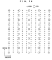
- Fig. 14 shows a positional relationship between the pixels of the 525i signal and the pixels of the 1080i signal.
- large dots are pixels of the 525i signal
- small dots are pixels of the 1080i signal.
- Solid lines express the positions of pixels in odd fields and broken lines express the positions of pixels in even fields.
- Fig. 15 shows a phase relationship in a vertical direction between the pixels of the 525i signal and the pixels of the 1080i signal.
- the numerical value assigned to each pixel of the 1080i signal means a shortest distance from the pixel of the 525i signal in a vertical direction.
- the interval between the pixels of the 525i signal in a vertical direction is set to 16.
- each of the numerical values assigned to each pixel of the 1080I signal shows phase information of this pixel in a vertical direction with respect to the pixel of the 525i signal.
- the phase information is set to a negative value when the pixel of the 1080i signal is located at a position upper than the pixel of the 525i signal (i.e. a pixel located at the shortest distance from this pixel of the 1080i signal), while it is set to a positive value when the pixel of the 1080i signal is located at a position lower than the pixel of the 525i signal.
- XGA extended graphics array
- Fig. 16 shows a phase relationship in a horizontal direction between the pixels of the 525i signal and the pixels of the 1080i signal.
- the numerical value assigned to each pixel of the 1080i signal means a shortest distance from the pixel of the 525i signal in a horizontal direction.
- the interval between the pixels of the 525i signal in a horizontal direction is set to 8.
- each of the numerical values assigned to the pixel of the 1080i signal shows phase information of this pixel in a horizontal direction with respect to the pixel of the 525i signal.
- the phase information is set to a negative value when the pixel of the 1080i signal is located at a position more left to the pixel of the 525i signal (i.e. a pixel located at the shortest distance from this pixel of the 1080i signal) while it is set to a positive value when the pixel of the 1080i signal is at a position more right to the pixel of the 525i signal.
- an input image signal is a 525i signal and an output image signal is an XGA signal.
- the XGA signal is an image signal in a progressive system (i.e. non-interlace system) available at a display with a resolution of 1024 ⁇ 768 dots.
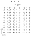
- Fig. 17 shows a positional relationship between the pixels of the 525i signal and the pixels of the XGA signal.
- large dots are pixels of the 525i signal
- small dots are pixels of the XGA signal.
- solid lines express the positions of pixels in odd fields and broken lines express the positions of pixels in even fields.
- Fig. 18 shows a phase relationship in a vertical direction between the pixels of the 525i signal and the pixels of the XGA signal.
- each of the numerical values assigned to the pixels of the XGA signal means a shortest distance from the pixel of the 525i signal in a vertical direction.
- the interval between the pixels of the 525i signal in a vertical direction is set to 16.
- each of the numerical values assigned to the pixels of the XGA signal shows phase information of this pixel in a vertical direction with respect to the pixel of the 525i signal.
- Fig. 19 shows a phase relationship in a horizontal direction between the pixels of the 525i signal and the pixels of the XGA signal.
- each of the numerical values assigned to the pixels of the XGA signal means a shortest distance from the pixel of the 525i signal in a horizontal direction.
- the interval between the pixels of the 525i signal in a horizontal direction is set to 8.
- each of the numerical values assigned to the pixels of the XGA signal shows phase information of this pixel in a horizontal direction with respect to the pixel of the 525i signal.
- phase relationship of the pixels of the output image signal to the pixels of the input image signal is uniquely determined, as is the case of the format conversion described above.
- the same phase relationship is obtained as the phase relationship between the 525i signal and the 1080i signal described above.
- EP 0 975 156 A2 describes a system for converting a 525i (interlace) signal into a 1050i-signal or a 525p (progressive) signal.
- a calculating circuit generates pixels of an output picture signal with a linear estimation expression of predictive taps received from a first tap selecting circuit and a coefficient received from a coefficient memory.
- the coefficient memory stores coefficients pre-obtained for individual classes.
- a class is determined by combining a spatial class corresponding to spatial class taps received from a second tap selecting circuit and motion class taps received from a third tap selecting circuit.
- a line sequential converting circuit converts a scanning line structure of an output signal of the calculating circuit and provides an output picture signal.
- the output picture signal is designated with a conversion method selection signal. Information corresponding to the selection signal is loaded from an information memory bank to the coefficient memory and registers.
- EP 1 001 353 A1 describes an interpolation processing technique that can be applied to image processing. Weighting coefficients for multiplication circuits are varied by a coefficient generation circuit based on phase information (x) of output data with respect to input data and a ratio (r) between the input sample number which forms the input data and an output sample number of corresponding output data.
- An objective of the present invention is to provide an information signal processor and the like which allows a memory for storing a large amount of coefficient data in order to make conversions into various formats or sizes to be eliminated.
- an information-providing medium in accordance with the present invention provides a computer program for executing each step in the method for processing the image signal described in claim 6.
- the conversion information about the format or size conversion is input and this conversion information is converted into the phase information about the target position in the second information signal.
- the information signal is a signal such as an image signal and a sound signal.
- the format or the image size after the conversion makes the phase relationship of the pixels of the output image signal to the pixels of the input image signal uniquely determined.
- the plurality of first information data located in periphery of the target position in the second information signal is selected according to the first information signal.
- the memory means stores the coefficient seed data, which is coefficient data in the production equation for producing the coefficient data to be used in the estimated equation.
- coefficient seed data is coefficient data in the production equation for producing the coefficient data to be used in the estimated equation.
- the memory stores no coefficient data corresponding to various formats and sizes so that there is no need of a memory for storing a large amount of coefficient data on the conversions into various formats or sizes are performed.
- a coefficient seed data production device in accordance with an example embodiment for producing coefficient seed data, the coefficient seed data being coefficient data in a production equation for producing coefficient data to be used in estimated equation employed when converting a first information signal including a plurality of information data into a second information signal including a plurality of information data, the production equation using phase information as a parameter, comprises signal processing means for performing a thinning-cut processing on a teacher signal to obtain a student signal, phase shift means for-shifting a phase of the student signal with a phase of information data position of the teacher signal being gradually changed with respect to the information data position of the student signal, first data selection means for selecting a plurality of first information data located in periphery of a target position in the teacher signal, based on the student signal having a phase shifted by the phase shift means, normal equation production means for producing a normal equation for obtaining the coefficient seed data using the plurality of the first information data selected by the first data selection means and the information data at the target position in the teacher signal, and coefficient seed data calculation means for
- a method for producing coefficient seed data in accordance with an example embodiment for producing coefficient seed data used for producing coefficient data to be used in an estimated equation employed when converting a first information signal including a plurality of information data into a second information signal including a plurality of information data, the coefficient seed data being coefficient data in a production equation using phase information as a parameter comprises a first step of performing a thinning-out processing on a teacher signal to obtain a student signal, a second step of shifting a phase of the student signal with the phase of information data position of the teacher signal being gradually changed with respect to the information data position of the student signal, a third step of selecting a plurality of information data located in periphery of a target position in the teacher signal, based on the student signal having a phase shifted in the second step, a fourth step of producing a normal equation for obtaining the coefficient seed data using the plurality of the information data selected in the third step and the information data at the target position in the teacher signal, and a fifth step of solving the normal equation produced in the fourth
- an information-providing medium in accordance with an example embodiment provides a computer program for executing each step in the method for producing the coefficient seed data described above.
- the thinning-out processing is performed on the teacher signal to obtain the student signal.
- the thinning-out processing is performed on the 1050i signal to obtain 525i signal as the student signal. Then, the phrase of the student signal is shifted with a phase of the information data position of the teacher signal being gradually changes with respect to the information data position of the student signal.
- a plurality of information data located in periphery of the target position in the teacher signal is selected on the basis of the phase-shifted student signal. Then, by use of thus-selected plurality of information data and the information data of the target position in the teacher signal, a normal equation for obtaining the coefficient seed data is produced. This equation is then solved to obtain the coefficient seed data.
- the coefficient seed data is coefficient data in the production equation for producing coefficient data to be used in the estimated equation employed when converting the first information signal into the second information signal, the production equation using the phase information as a parameter.
- this coefficient seed data allows the coefficient data corresponding to arbitrary phase information to be obtained according to the production equation.
- the coefficient data of the estimated equation is produced from the coefficient seed data on the basis of the phase information about the target position in the second information signal so that it can obtain the information data of the target position using thus-produced coefficient data.
- a coefficient seed data production device in accordance with an example embodiment for producing coefficient seed data, the coefficient seed data being coefficient data in production equation for producing coefficient data to be used in estimated equation employed when converting a first information signal including a plurality of information data into a second information signal including a plurality of information data, and the production equation using phase information as a parameter, comprises signal processing means for performing a thinning-out processing on a teacher signal to obtain a student signal, phase shift means for shifting a phase of the student signal with a phase of information data position of the teacher signal being gradually changed with respect to the information data position of the student signal, first data selection means for selecting a plurality of first information data located in periphery of a target position in the teacher signal, based on the student signal having a phase shifted by the phase shift means, first normal equation production means for producing a first normal equation for obtaining the coefficient data of the estimated equation per phase shift value of the student signal using the plurality of the first information data selected in the first data selection means and the information data at the target position in the
- a method for producing coefficient seed data in accordance with an example embodiment for producing coefficient seed data comprises a first step of performing a thinning-out processing on a teacher signal to obtain a student signal, a second step of shifting a phase of the student signal with a phase of information data position of the teacher signal being gradually changed with respect to the information data position of the student signal, a third step of selecting a plurality of information data located in periphery of a target position in the teacher signal, based on the student signal having a phase shifted in the second step, a fourth step of producing a first normal equation for obtaining the coefficient data of the estimated equation per phase shift value of the student signal using the plurality of the information data selected in the third step and the information data at the target position in the teacher signal
- an information-providing medium in accordance with an example embodiment provides a computer program for executing each step in the method for producing the coefficient seed data described above.
- the thinning-out processing is performed on the teacher signal to obtain the student signal.
- the thinning-out processing is performed on the 1050i signal to obtain 525i signal as the student signal. Then, the phase of the student signal is shifted with the phase of the information data position of the teacher signal being gradually changes with respect to the information data position of the student signal.
- a plurality of information data located in periphery of the target position in the teacher signal is selected on the basis of the phase-shifted student signal. Then, by use of thus-selected plurality of information data and the information data of the target position in the teacher signal, a first normal equation for obtaining the coefficient data of the estimated equation is produced at every phase shift value of the student signal. This equation is then solved to obtain coefficient data of the estimated equation at every phase shift value.
- the coefficient seed data is coefficient data in the production equation for producing the coefficient data to be used in the estimated equation employed when converting the first information signal into the second information signal, the production equation using the phase information as parameter.
- Using this coefficient seed data allows the coefficient data corresponding to arbitrary phase information to be obtained according to the production equation.
- the coefficient data of the estimated equation is produced according to the coefficient seed data based on the phase information about the target position in the second information signal. Then, by use of thus-produced coefficient data, it becomes possible to obtain the information data of the target position.
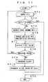
- Fig. 1 shows a configuration of television receiver 100 as an embodiment.
- the television receiver 100 receives a 525i signal from a broadcast signal and converts the 525i signal into a 1080i signal or a XGA signal so as to display an image, or converts the 525i signal into a new 525i signal for partially magnifying the image by an arbitrary magnification and displaying the partially magnified image.
- the television receiver 100 comprises a system controller 101 with a microcomputer for controlling operations of the entire system, and a remote control signal receiving circuit 102 for receiving a remote control signal.
- the remote control signal receiving circuit 102 is connected to the system controller 101, and it is constituted so as to receive a remote control signal RM from a remote control transmitter 200 in accordance with the user operation and to supply an operation signal corresponding to the received signal RM to the system controller 101.
- the television receiver 100 also comprises a receiving antenna 105, a tuner 106 for receiving a broadcast signal (RF modification signal) captured by the receiving antenna 105, and performing processing such as a channel selection, a middle frequency amplification, and a wave detection so as to obtain a 525i signal, and a buffer memory 109 for temporarily storing the 525i signal output from the tuner 106.
- a broadcast signal RF modification signal
- the television receiver 100 further comprises an image signal processing section 110 for using the 525i signal temporarily stored in the buffer memory 109 as an input image signal Vin and converting the 525i signal into a 1080i signal or a XGA signal, or converting it into a new 525i signal for partially magnifying the image by an arbitrary magnification and displaying the partially magnified image, and then transmitting the resultant signal, and a display section 111 for displaying an image produced by the output image signal Vout received from the image signal processing section 110.
- the display section 111 is constituted by, for example, a display apparatus such as a cathode-ray tube (CRT) display, a liquid crystal display (LCD).
- the 525i signal transmitted from the tuner 106 is supplied to the buffer memory 109, which temporarily stores it.
- the 525i signal stored in the buffer memory 109 is supplied to the image signal processing section 110 as an input image signal Vin.
- the 525i signal as the input image signal Vin is converted into a 1080i signal or a XGA signal, or the 525i signal is converted into a new 525i signal for partially magnifying the image by an arbitrary magnification and displaying the partially magnified image.
- the output image signal Vout transmitted from the image signal processing section 110 is supplied to the display section 111, which displays an image produced by the output image signal Vout on the screen thereof.
- the image signal processing section 110 includes first to third tap selection circuits 121 to 123 each for selectively extracting a plurality of pixel data located in periphery of each pixel (target pixel) within a unit pixel block constituting the output image signal Vout from the 525i signal stored in the buffer memory 109, and then transmitting them.
- the first tap selection circuit 121 selectively extracts data of the pixel for use in prediction (hereinafter, referred to as "prediction tap”).
- the second tap selection circuit 122 selectively extracts data of the pixel for use in sorting space classes (hereinafter, referred to as “space class tap”).
- the third tap selection circuit 123 selectively extracts data of pixel for use in sorting movement classes (hereinafter, referred to as "movement class tap"). Where the space class is determined using the pixel data belonging to the plural fields, this space class also contains information about movements.
- the image signal processing section 110 also includes a space class detection circuit 124 for detecting a distribution pattern of levels of data of space class tap (two or more) selectively extracted in the second tap selection circuit 122, and detecting a space class based on the distribution pattern of the levels so as to transmit information about the class.
- a space class detection circuit 124 for detecting a distribution pattern of levels of data of space class tap (two or more) selectively extracted in the second tap selection circuit 122, and detecting a space class based on the distribution pattern of the levels so as to transmit information about the class.
- the space class detection circuit 124 performs an operation such that, for example, the space class tap data is compressed from 8 bit-data into 2 bit-data. Then, the space class detection circuit 124 transmits the compressed data each corresponding to the space class tap data as class information of the space class.
- data compression is performed according to an adaptive dynamic range coding (ADRC) method.
- ADRC adaptive dynamic range coding
- DPCM differential pulse code modulation
- VQ vector quantization
- ADRC is an adaptive re-quantization method, which has been developed for use in high performance coding for video tape recorder (VTR).
- VTR video tape recorder
- the ADRC is also preferable to a case used in the data compression described above because this method is capable of effectively expressing a local pattern of a signal level in a short language.
- the portion enclosed with [] means truncation process.
- i is set to to Na.
- the image signal processing section 110 also includes an movement class detection circuit 125 for detecting a movement class for mainly expressing the degree of movement, from the movement class tap data (two or more) selectively extracted in the third tap selection circuit 123, and then transmitting the class information thereof.
- a differential between frames is calculated from the movement class tap data selectively extracted in the third tap selection circuit 123. Then, a threshold value processing is performed on an average value of the absolute values of differentials so that the movement class, which is an index of movement, can be detected. Specifically, in the movement class detection circuit 125, an average value AV of the absolute values of the differentials is calculated in following Equation (2).
- Nb in the Equation (2) is 6.
- the average value AV calculated as described above is compared with one or a plurality of threshold values so as to allow class information MV about movement class to be obtained. For example, when three threshold values th1, th2, th3 (th1 ⁇ th2 ⁇ th3) are prepared and four movement classes are to be detected, MV is set to 0 when AV ⁇ th1; MV is set to 1 when th1 ⁇ AV ⁇ th2; MV is set to 2 when th2 ⁇ AV ⁇ th3; and MV is set to 3 when th3 ⁇ AV.
- the image signal processing section 110 also includes a class synthesis circuit 126 for obtaining a class code CL showing a class including the data of each pixel (target pixel) within the unit pixel block constituting the output image signal Vout to be produced, based on the re-quantized code qi as class information about the space class received from the space class detection circuit 124 and the class information MV about the movement class received from the movement class detection circuit 125.
- the class code CL is calculated in following Equation (3).
- CL ⁇ i 1 Na qi 2 P i 1 + MV ⁇ 2 P Na
- Na indicates the number of space class tap data
- P indicates the re-quantized bit number in ADRC method.
- the image signal processing section 110 also includes registers 130 to 133 and a coefficient memory 134.
- a post-processing circuit 129 which will be described later, is required to change its operation among the case where a 1080i signal is transmitted as the output image signal Vout, the case where an XGA signal is transmitted as the output image signal Vout, and the case where a 525i signal is transmitted as the output image signal Vout.
- the register 130 stores operation specifying information for specifying operations of the post-processing circuit 129.
- the post-processing circuit 129 exhibits the operations in compliance with the operation specifying information supplied from the register 130.
- the register 131 stores information about the tap position of the prediction tap to be selected in the first tap selection circuit 121.
- the first tap selection circuit 121 selects the prediction tap in compliance with the tap position information supplied from the register 131.
- the tap position information assigns numbers to the plurality of pixels which may be selected for example, and specifies the number of pixel to be selected.
- the tap position information described hereinafter also performs the same operation as described above.
- the register 132 stores tap position information of the space class tap to be selected in the second tap selection circuit 122.
- the second tap selection circuit 122 selects the space class tap in compliance with the tap position information supplied from the register 132.
- the register 132 stores tap position information A of the case where a movement is relatively small, and tap position information B of the case where a movement is relatively large. Which of the tap position information A or B is to be supplied to the second tap selection circuit 122 is determined by the class information MV of the movement class transmitted from the movement class detection circuit 125.
- the tap position information A is supplied to the second tap selection circuit 122.
- the space class tap selected in the second tap selection circuit 122 is made to extend over plural fields. Contrarily, if MV is 2 or MV is 3 because the movement is relatively large, the tap position information B is supplied to the second tap selection circuit 122.
- the space class tap selected in the second tap selection circuit 122 is made to be only the pixel within the field where the pixel to be produced is present.
- the register 131 described above also stores the tap position information of the case where the movement is relatively small and the tap position information of the case where the movement is relatively large, so that the tap position information to be supplied to the first tap selection circuit 121 can be selected by the class information MV of the movement class transmitted from the movement class detection circuit 125.
- the register 133 stores the tap position information of the movement class tap to be selected in the third tap selection circuit 123.
- the third tap selection circuit 123 selects a movement class tap in compliance with the tap position information supplied from the register 133.
- the coefficient memory 134 stores, for each class, the coefficient data of the estimated equation to be used in an estimated prediction calculation circuit 127, which will be described later.
- the coefficient data is information for converting the 525i signal into the 1080i signal or the XGA signal, or for converting the 525i signal into a new 525i signal for partially magnifying the image by an arbitrary magnification and displaying the partially magnified image.
- the coefficient memory 134 receives the class code CL from the class synthesis circuit 126 described above as read address information. Coefficient data corresponding to the class code CL is read out of the coefficient memory 134, and thus read coefficient data is supplied to the estimated prediction calculation circuit 127.
- the image signal processing section 110 also includes an information memory bank 135.
- information memory bank 135 movement specifying information to be stored into the register 130 and the tap position information to be stored in the registers 131 to 133 are stored beforehand.
- first movement specifying information for operating the post-processing circuit 129 to transmit the 1080i signal is stored beforehand in the information memory bank 135.
- second movement specifying information for operating the post-processing circuit 129 to transmit the XGA signal is stored beforehand in the information memory bank 135.
- third movement specifying information for operating the post-processing circuit 129 to transmit the 525i signal are stored beforehand in the information memory bank 135.
- the user can make selection among the first conversion method for transmitting the 1080i signal, the second conversion method for transmitting the XGA signal, or the third conversion method for transmitting the 525i signal, by operating the remote control transmitter 200.
- the user can further specify the magnification (the image size) of the image to be displayed.
- the information memory bank 135 receives the selection information about the conversion method to be selected from the system controller 101.
- the information memory bank 135 loads the first, second, or third movement specifying information in compliance with the received selection information into the register 130.
- first tap position information corresponding to the first conversion method (1080i), second tap position information corresponding to the second conversion method (XGA), and third tap position information corresponding to the third conversion method (525i), are stored beforehand as the tap position information of the prediction tap to be stored in the register 131.
- the information memory bank 135 loads the first, second, or third tap position information into the register 131 in compliance with the selection information about the conversion method described above.
- tap position information corresponding to the magnification of the image to be displayed is stored into the information memory bank 135 beforehand as the third tap position information corresponding to the third conversion method, and at the same time when the third conversion method is selected, the tap position information corresponding to the specified magnification is loaded from the information memory bank 135 into the register 131.
- the tap information is loaded into registers 132 and 133, which will be described later.
- the first tap position information corresponding to the first conversion method (1080i), the second tap position information corresponding to the second conversion information (XGA), and the third tap position information corresponding to the third conversion method (525i) are stored beforehand in the information memory bank 135 as tap position information of the space class tap to be stored into the register 132.
- the first, second, and third tap position information is respectively constituted by tap position information for the case where a movement is relatively small, and tap position information for the case where a movement is relatively large.
- the first, second, or third tap position information is loaded from the information memory bank 135 into the register 132 in compliance with the selection information about the conversion method described above.
- first tap position information corresponding to the first conversion method (1080i), the second tap position information corresponding to the second conversion method (XGA), and the third tap position information corresponding to the third conversion method (525i) are stored beforehand in the information memory bank 135 as tap position information of the movement class tap to be stored in the register 133.
- the first, second, or third tap position information is loaded from the information memory bank 135 into the register 133 in compliance with the selection information about the conversion method described above.
- the information memory bank 135 stores coefficient seed data of each class beforehand.
- the coefficient seed data is coefficient data of the production equation for producing coefficient data to be stored into the coefficient memory 134 described above, the production equation using the phase information as a parameter.
- pixel data y to be produced is calculated according to the estimated equation of Equation (4) from prediction tap data xi and the coefficient data Wi read out of the coefficient memory 134.
- n in the Equation (4) is 10.
- W 1 w 10 + w 11 ⁇ v + w 12 ⁇ h + w 13 ⁇ v 2 + w 14 ⁇ vh + w 15 ⁇ h 2 + w 16 ⁇ v 3 + w 17 ⁇ v 2 ⁇ h + w 18 ⁇ vh 2 + w 19 ⁇ h 3
- coefficient seed data W 10 to W n9. which is coefficient data of this production equation, is stored per class. The method for producing the coefficient seed data will be described later.
- the coefficient seed data of each class is loaded into this coefficient production circuit 136 from the information memory bank 135.
- the phase information h, v in the horizontal direction and the vertical direction of each pixel within the unit pixel block constituting the output image signal Vout generated in a phase information generation circuit 139, which will be described later, is supplied to the coefficient production circuit 136.
- the image signal processing section 110 also includes a phase information generation circuit 139 for generating the phase information h, v in the horizontal direction and the vertical direction of each pixel within the unit pixel block constituting the output image signal Vout, based on the selection information about the conversion method and the corresponding function information n/m relating to the number of pixels in each field in the vertical direction and in the horizontal direction in the input image signal Vin and the output image signal Vout corresponding to the information for specifying the magnification, which are received from the system controller 101.
- This phase information generation circuit 139 is constituted by a ROM table, for example.
- phase information h, v in the horizontal direction and the vertical direction of each pixel generated in the phase information generation circuit 139 is respectively associated with the pixel number (tap number) and then supplied to the coefficient production circuit 136.
- the phase information generation circuit 139 generates the phase information h, v corresponding to the respective odd and even fields of the input image signal Vin.
- n/m is 9/4 as to the vertical direction
- n/m is 9/4 as to the horizontal direction (see Fig. 14 ).
- the 9 ⁇ 9 pixel block of the 1080i signal as the output image signal Vout corresponds to the 4 ⁇ 4 pixel block of the 525i signal as the input image signal Vin.
- the unit pixel block constituting the output image signal Vout is a 9x9 pixel block.
- phase information generation circuit 139 as to each pixel within this 9x9 unit pixel block, a distance between pixels located at positions closest to each other in the vertical direction (pixels at a shortest distance) is obtained among the pixels within the 4 ⁇ 4 pixel block of the 525i signal described above, and the obtained value of the distance is used as phase information v; and a distance between pixels located at positions closest to each other in the horizontal direction (pixels at a shortest distance) is obtained, and the obtained value of the distance is used as phase information h.
- the phase information h, v described above is obtained under the condition where the interval between pixels in the vertical direction of the 525i signal is set to 16, and the interval between pixels in the horizontal direction thereof is set to 8. The same thing is applied to the case where the second and third conversion methods are selected respectively.
- the phase information v is set to a negative value when the target pixel within the 9 ⁇ 9 unit pixel block is located at a position upper than the pixel at the shortest distance. Contrarily, the phase information v is set to a positive value when the target pixel within the 9 ⁇ 9 unit pixel block is located at a position lower than the pixel at the shortest distance described above.
- the phase information h is set to a negative value when the target pixel thereof is located at a position left of the pixel at the shortest distance. Contrarily, the phase information h is set to a positive value when the target pixel thereof is located at a position right of the pixel at the shortest distance. The same thing is applied to the case where the second and third conversion methods are selected, respectively.
- the phase information generation circuit 139 when the first conversion method (1080i) is selected, in the phase information generation circuit 139, the phase information h, v is generated for each of 81 pixels, which constitute the 9 ⁇ 9 unit pixel block, in correspondence with the respective odd and even fields.
- n/m is 16/5 as to the vertical direction
- n/m is 8/5 as to the horizontal direction (see Fig. 17 ).
- the 8 ⁇ 16 pixel block of the XGA signal as the output image signal Vout corresponds to the 5 ⁇ 5 pixel block of the 525i signal as the input image signal Vin.
- the unit pixel block constituting the output image signal Vout is a 8 ⁇ 16 pixel block.
- phase information generation circuit 139 as to each pixel within this 8 ⁇ 16 unit pixel block, a distance between pixels located at positions closest to each other in the vertical direction (pixels at a shortest distance) is obtained among the pixels within the 5 ⁇ 5 pixel block of the 525i signal described above, and the obtained value of the distance is used as phase information v; and a distance between pixels located at positions closest to each other in the horizontal direction (pixels at a shortest distance) is obtained, and the obtained value of the distance is used as phase information h.
- phase information generation circuit 139 when the second conversion method (XGA) is selected, in the phase information generation circuit 139, the phase information h, v is generated for each of 128 pixels, which constitute the 8 ⁇ 16 unit pixel block, in correspondence with the respective odd and even fields.
- the values of n/m in the vertical direction and in the horizontal direction are uniquely determined in correspondence with the specified magnification of the image to be displayed (the image size).
- n/m is nv/mv as to the vertical direction
- n/m is nh/mh as to the horizontal direction
- nh ⁇ nv pixel block of the 525i signal as the output image signal Vout corresponds to the mh ⁇ mv pixel block of the 525i signal as the input image signal Vin.
- the unit pixel block constituting the output image signal Vout is a nhxnv pixel block.
- phase information generation circuit 139 as to each pixel within this nh ⁇ nv unit pixel block, a distance between pixels located at positions closest to each other in the vertical direction (pixels at a shortest distance) is obtained among the pixels within the mh ⁇ mv pixel block of the 525i signal as the input image signal Vin described above, and the obtained value of the distance is used as phase information v; and a distance between pixels located at positions closest to each other in the horizontal direction (pixels at a shortest distance) is obtained, and the obtained value of the distance is used as phase information h.
- the phase information generation circuit 139 when the third conversion method (525i) is selected, in the phase information generation circuit 139, the phase information h, v is generated for each of the pixels, which constitute the nh ⁇ nv unit pixel block, in correspondence with the respective odd and even fields.
- the normalized coefficient memory 138 receives the class code CL from the aforementioned class synthesis circuit 126 as read address information.
- the normalized coefficient S corresponding to the class code CL is read out of the normalized coefficient memory 138, and then thus read normalized coefficient S is supplied to a normalized calculation circuit 128, which will be described later.
- the image signal processing section 110 also includes the estimated prediction calculation circuit 127 for calculating data of each pixel within the unit pixel block constituting the output image signal Vout, based on the prediction tap data xi selectively extracted in the first tap selection circuit 121 and the coefficient data Wi read out of the coefficient memory 134.
- this estimated prediction calculation circuit 127 pixel data constituting the output image signal Vout is produced for every unit pixel block. Specifically, the estimated prediction calculation circuit 127 receives the prediction tap data xi corresponding to each pixel within the unit pixel block (target pixel) from the first tap selection circuit 121 and the coefficient data Wi corresponding to each pixel constituting the unit pixel block from the coefficient memory 134. The data of each pixel constituting the unit pixel block is calculated separately according to the estimated equation of the aforementioned Equation (4).
- the estimated prediction calculation circuit 127 when the first conversion method (1080i) is selected, data of 81 pixels constituting the unit pixel block is simultaneously produced; when the second conversion method (XGA) is selected, data of 128 pixels constituting the unit pixel block is simultaneously produced; and when the third conversion method (525i) is selected, data of pixels in the number of (nhxnv) constituting the unit pixel block (the values of nh and nv change in accordance with the specified magnification of the image to be displayed) is simultaneously produced.
- P shows the number of pixels constituting the unit block
- the coefficient production circuit 136 produces the coefficient data of the estimated equation from the coefficient seed data according to the production equation
- the image signal processing section 110 also includes the post-processing circuit 129 for processing the data y 1 ' to y p ' of the pixels within the unit pixel block normalized in the normalized calculation circuit 128 and sequentially received therefrom, and transmitting the output image signal Vout with the format specified by any one of the first to third conversion methods.
- the post-processing circuit 129 transmits the 1080i signal when the first conversion method is selected, transmits the XGA signal when the second conversion method is selected, and transmits the 525i signal when the third conversion method is selected.
- the information for specifying the operation of the post-processing circuit 129 is supplied from the register 130 as described above.
- the second tap selection circuit 122 space class tap data (pixel data) located in periphery of each pixel (target pixel) within the unit pixel block constituting the output image signal Vout to be produced is selectively extracted from the 525i signal stored in the buffer memory 109 as the input image signal Vin.
- the selection of tap is performed, based on the conversion method supplied from the register I32 and selected by the user, and the tap position information corresponding to the movement class detected in the movement class detection circuit 125.
- each pixel data as the space class tap data is subjected to an ADRC processing so that a re-quantized code qi as class information of the space class (a class sort mainly for the purpose of expressing the waveform in a space) may be obtained (see the Equation (1)).
- movement class tap data located in periphery of the pixels within the unit pixel block (target pixel) constituting the output image signal Vout to be produced is selectively extracted from the 525i signal stored in the buffer memory 109 as the input image signal Vin.
- the selection of tap is performed on the basis of the tap position information selected by the user and supplied from the register 133, the tap position information corresponding to the conversion method.
- the coefficient data Wi in each phase information corresponding to the class code CL is read out of the coefficient memory 134 and then thus read coefficient data Wi is supplied to the estimated prediction calculation circuit 127.
- prediction tap data pixel data located in periphery of each pixel (target pixel) within the unit pixel block constituting the output image signal Vout to be produced is selectively extracted from the 525i signal stored in the buffer memory 109 as the input image signal Vin.
- the selection of tap is performed on the basis of the tap position information corresponding to the conversion method selected by the user and supplied from the register 131.
- the prediction tap data xi is supplied to the estimated prediction calculation circuit 127.
- the estimated prediction calculation circuit 127 data y 1 to y p of each pixel within the unit pixel block constituting the output image signal Vout to be produced is simultaneously calculated, from the prediction tap data xi and the coefficient data Wi in each phase information read out of the coefficient memory 134 (see the Equation (4)).
- the class code CL is supplied to the normalized coefficient memory 138 as read address information.
- read is the normalized coefficient S corresponding to the class code CL, that is, the normalized coefficient S corresponding to the coefficient data Wi which has been used in calculating the data y 1 to y p output from the estimated prediction calculation circuit 127.
- read normalized coefficient S is supplied to the normalized calculation circuit 128.
- the data y 1 to y p transmitted from the estimated prediction calculation circuit 127 is normalized with dividing them by their respectively corresponding normalized coefficients S. This removes the level fluctuation of the data y 1 to y p caused by rounding error occurred when the coefficient data of the estimated equation (see the Equation (4)) is obtained according to the production equation (see the Equation (5)) using the coefficient seed data.
- the post-processing circuit 129 receives the data y 1 ' to y p ' and transmits them with a format specified by any one of the first to third conversion methods as the output image signal Vout.
- the first conversion method is selected, the 1080i signal is transmitted as the output image signal Vout.
- the XGA signal is transmitted as the output image signal Vout.
- the 525i signal is transmitted as the output image signal Vout.
- coefficient data Wi of the estimated equation corresponding to the values of the phase information h, v is produced per class using the coefficient seed data in each class loaded from the information memory bank 135 and the values of the phase information h, v generated in the phase information generation circuit 139. Then, the resultant coefficient data Wi is stored into the coefficient memory 134. Then, by use of the coefficient data Wi in each phase information read out of the coefficient memory 134 in correspondence with the class code CL, the data y 1 to y p of each pixel within the unit pixel block constituting the output image signal Vout is calculated in the estimated prediction calculation circuit 127. Consequently, this eliminates needs of a memory for storing a large amount of coefficient data when a format conversion into the 1080i signal or the XGA signal is performed, or a conversion into various image sizes is performed.
- the coefficient seed data is stored per class in the information memory bank 135. This coefficient seed data is produced beforehand by learning.
- an undefined coefficient w ij is obtained by the leaning.
- this is a solution method by use of a least square method where a coefficient value which minimizes a square error is defined per class using pixel data of a student signal and pixel data of a teacher signal. Defining the number of learning as m, a residual error at k-th learning data (1 ⁇ k ⁇ m) as e k , and a sum of square errors as E, E is expressed in following Equation (9) by use of the Equations (4) and (5).
- the term x ik shows k-th pixel data at a position of i-th prediction tap of the student image
- the term y k shows k-th pixel data of the teacher image corresponding thereto.
- Equation (10) can be rewritten into following Equation (13) by use of matrix.
- This equation is generally referred to as a normal equation.
- the normal equation is solved about w ij by use of a sweeping method
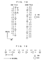
- Fig. 4 shows the states of phase shifts V1 to V8 into eight stages in a vertical direction.
- the interval between pixels of the SD signal in the vertical direction is 16, and the downward direction is set to a positive direction.
- the term "o" expresses an odd field
- e expresses an even field.
- the shift amount of the SD signal is set to 0.
- the pixels of the HD signal come to have phases of 4, 0, -4, and -8 with respect to the pixels of the SD signal.
- the shift amount of the SD signal is set to 1.
- the pixels of the HD signal come to have phases of 7, 3, -1, and -5 with respect to the pixels of the SD signal.
- the shift amount of the SD signal is set to 2.
- the pixels of the HD signal come to have phases of 6, 2, -2, and -6 with respect to the pixels of the SD signal.
- the shift amount of the SD signal is set to 3.
- the pixels of the HD signal come to have phases of 5, 1, -3, and -7 with respect to the pixels of the SD signal.
- the shift amount of the SD signal is set to 4.
- the pixels of the HD signal come to have phases of 4, 0, -4, and -8 with respect to the pixels of the SD signal.
- the shift amount of the SD signal is set to 5.
- the pixels of the HD signal come to have phases of 7, 3, -1, and -5 with respect to the pixels of the SD signal.
- the shift amount of the SD signal is set to 6.
- the pixels of the HD signal come to have phases of 6, 2, -2, and -6 with respect to the pixels of the SD signal.
- the shift amount of the SD signal is set to 7.
- the pixels of the HD signal come to have phases of 5, 1, -3, and -7 with respect to the pixels of the SD signal.
- Fig. 5 shows the states of phase shifts H1 to H4 into four stages in a horizontal direction.
- the interval between pixels of the SD signal in the horizontal direction is set to 8
- the right direction is set to a positive direction.
- the shift amount of the SD signal is set to 0.
- the pixels of the HD signal come to have phases of 0, and -4 with respect to the pixels of the SD signal.
- the shift amount of the SD signal is set to 1.
- the pixels of the HD signal come to have 3, and -1 with respect to the pixels of the SD signal.
- the shift amount of the SD signal is set to 2.
- the pixels of the HD signal come to have phases of 2, and -2 with respect to the pixels of the SD signal.
- the shift amount of the SD signal is set to 3.
- the pixels of the HD signal come to have phases of 1, and -3 with respect to the pixels of the SD signal.
- Fig. 6 shows the phases of the pixels of the HD signal in a case where the pixels of the SD signal are located at center positions, as to 32 kinds of SD signals obtained as a result of shifting the phase of the SD signal into 8 stages in the vertical direction and into 4 stages in the horizontal direction as described above.
- the pixels of the HD signal come to have phases expressed by ⁇ in Fig. 6 with respect to the pixels of the SD signal.
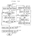
- Fig. 7 shows a configuration of a coefficient seed data production device 150 for producing the coefficient seed data, based on the concept described above.
- the coefficient seed data production device 150 includes an input terminal 151 for receiving the HD signal (1050i signal) as a teacher signal, an SD signal production circuit 152A for performing a thinning-out processing on the HD signal in horizontal and vertical directions so as to obtain the SD signal as an input signal, and a phase shift circuit 152B for shifting the phase of the SD signal into 8 stages in the vertical direction and into 4 stages in the horizontal direction so as to obtain the SD signals SD 1 to SD 32 in 32 kinds in total.
- the phase shift circuit 152B receives parameters H, V for specifying the values of the phase shifts in the vertical direction and in the horizontal direction.
- the phase shift circuit 152B is constituted by, for example, a filter having a characteristic of sinx/x; however, it is also possible to employ another kind of filter which enables phase shift. As an example of another kind of filter, there is a method where only a desired phase is extracted from an over sampling filter, or the like.
- the coefficient seed data production device 150 also includes first to third tap selection circuits 153 to 155 each for selectively extracting the data of a plurality of SD pixels located in periphery of the target position in the HD signal (1050i signal) from the SD signals SD 1 to SD 32 received from the phase shift circuit 152B, and then transmits the extracted data.
- These first to third tap selection circuits 153 to 155 are constituted so as to have the same structures as those of the first to third tap selection circuits 121 to 123 in the image signal processing section 110 described above.
- the taps selected in the fist to third tap selection circuits 153 to 155 are specified by the tap position information provided from a tap selection control section 156.
- the class information MV of the movement class output from a movement class detection circuit 158 which will be described later, is supplied to the tap selection control circuit 156.
- the tap position information to be supplied to the second tap selection circuit 154 is differed depending on whether a movement is large or small.
- the coefficient seed data production apparatus 150 also includes a space class detection circuit 157 for detecting the distribution pattern of the levels of the space class tap data (SD pixel data) selectively extracted in the second tap selection circuit 154, detecting a space class based on the distribution pattern of levels, and then transmitting the class information thereof.
- the space class detection circuit 157 is constituted so as to have the same structure as that of the space class detection circuit 124 in the image signal processing section 110 described above.
- the space class detection circuit 157 transmits, as class information showing the space class, a re-quantized code qi for each SD pixel data as the space class tap data.
- the coefficient seed data production apparatus 150 also includes the movement class detection circuit 158 for detecting a movement class mainly showing the degree of movement from the class tap data (SD pixel data) selectively extracted in the third tap selection circuit 155, and then transmitting the class information MV thereof.
- the movement class detection circuit 158 is constituted so as to have the same structure as that of the movement class detection circuit 125 in the image signal processing section 110 described above.
- a differential between frames is calculated from the movement class tap data (SD pixel data) which is selectively extracted in the third tap selection circuit 155. Then, a threshold value processing is performed on an average value of the absolute values of differentials so that the movement class, which is an index of movement, can be detected.
- the coefficient seed data production apparatus 150 also includes a class synthesis circuit 159 for obtaining a class code CL showing a class including the pixel data at the target position in the HD signal (1050i signal), based on the re-quantized code qi as class information about the space class received from the space class detection circuit 157 and the class information MV about the movement class received from the movement class detection circuit 158.
- the class synthesis circuit 159 is also constituted so as to have the same structure as that of the class synthesis circuit 126 in the image signal processing section 110 described above.
- the coefficient seed data production apparatus 150 also includes a normal equation production section 160 for producing a normal equation (see the Equation (13)) to be employed for obtaining coefficient seed data w 10 to w n9 for each class, from each HD pixel data y as pixel data at the target position obtained from the HD signal received at the input terminal 151, prediction tap data (SD pixel data) xi selectively extracted in the first tap selection circuit 153 respectively in correspondence with each HD pixel data y, and the class code CL received from the class synthesis circuit 159 respectively in correspondence with each HD pixel data y, and the parameters H, V of the phase shift values in the vertical direction and in the horizontal direction.
- a normal equation production section 160 for producing a normal equation (see the Equation (13)) to be employed for obtaining coefficient seed data w 10 to w n9 for each class, from each HD pixel data y as pixel data at the target position obtained from the HD signal received at the input terminal 151, prediction tap data (SD pixel data) xi selectively extracted in the
- learning data is produced in combination of one HD pixel data y and the prediction tap pixel data in the number of n corresponding to the HD pixel data y.
- the parameters H, V to be supplied to the phase shift circuit 152B are sequentially changed so that 32 kinds of SD signals SD 1 to SD 32 , having gradually-changed phase shift values can be sequentially produced.
- a normal equation in which a large number of learning data are registered is produced in the normal equation production section 160.
- the timing of the SD pixel data xi supplied from the first tap selection circuit 153 to the normal equation production section 160 can be adjusted.
- the coefficient seed data production apparatus 150 also includes a coefficient seed data decision section 161 for receiving data of the normal equation produced for each class in the normal equation production section 160, and solving the normal equation for each class so as to obtain the coefficient seed data w 10 to w n9 in each class, and a coefficient seed memory 162 for storing thus-obtained coefficient seed data w 10 to w n9 .
- the normal equation is solved according to a method such as sweeping so that the coefficient data w 10 to w n9 can be obtained.
- the coefficient seed data production apparatus 150 shown in Fig. 7 An operation of the coefficient seed data production apparatus 150 shown in Fig. 7 will be described.
- the input terminal 151 receives an HD signal (1050i signal) as a teacher signal
- the HD signal is subjected to the thinning-out processing in horizontal and vertical directions on the SD signal production circuit 152A so that an SD signal (525i signal) as a student signal can be produced.
- SD signal is supplied to the phase shift circuit 152B, which shifts the phase of the SD signal into 8 stages in the vertical direction and into 4 stages in the horizontal direction (see Figs. 4 and 5 ), so that 32 kinds of SD signals SD 1 to SD 32 can be sequentially produced.
- space class tap data (SD pixel data) located in periphery of the target position in the HD signal is selectively extracted from these SD signals SD 1 to SD 32 -
- the selection of tap is performed, based on the tap position information supplied from the tap selection control circuit 156, the tap position information corresponding to the movement class detected in the movement class detection circuit 158.
- the resultant space class tap data (SD pixel data) is supplied to the space class detection circuit 157.
- each SD pixel data as the space class tap data is subjected to ADRC processing so that a re-quantized code qi as class information of the space class (a class sort mainly for the purpose of expressing the waveform in a space) can be produced (see the Equation (1)).
- movement class tap data (SD pixel data) located in periphery of the target position in the HD signal is selectively extracted from the SD signals SD 1 to SD 32 obtained in the phase shift circuit 152B.
- the selection of the tap is performed, based on the tap position information supplied from the tap selection control circuit 156.
- the movement class detection circuit 158 receives movement class tap data (SD pixel data) from the movement class detection circuit 158.
- the class information MV about the movement class (a class sort mainly for the purpose of expressing the degree of movement) is obtained from each SD pixel data as movement class tap data.
- the class synthesis circuit 159 the class code CL showing a class including pixel data at the target position in the HD signal is obtained from the movement information MV and the re-quantized code qi (see the Equation (3)).
- the prediction tap data (SD pixel data) located in periphery of the target position in the HD signal is selectively extracted from the SD signals SD 1 to SD 32 produced in the phase shift circuit 152B.
- the selection of tap is performed, based on the tap position information supplied from the tap selection control circuit 156.
- a normal equation (see the Equation (13)) to be employed for obtaining coefficient the seed data w 10 to w n9 is produced for each class, from each HD pixel data y as pixel data at the target position obtained from the HD signal received at the input terminal 151, prediction tap data (SD pixel data) xi selectively extracted in the first tap selection circuit 153 respectively in correspondence with each HD pixel data y, the class code CL received from the class synthesis circuit 159 respectively in correspondence with each HD pixel data y, and the parameters H, V of the phase shift values in the vertical direction and in the horizontal direction.
- the normal equation is solved in the coefficient seed data decision section 161 so that the coefficient seed data w 10 to w n9 for each class can be obtained.
- the coefficient seed data w 10 to w n9 is stored in the coefficient seed memory 162 in which addresses are assigned for each class.
- the coefficient seed data production device 150 shown in Fig. 7 it is possible to produce the coefficient seed data w 10 to w n9 for each class stored in the information memory bank 135 of the image signal processing section 110 shown in Fig. 1 .
- Fig. 8 shows a concept of this example.
- the SD signal is shifted into 8 stages in the vertical direction and is shifted into 4 stages into the horizontal direction by the parameters H, V, so that 32 kinds of SD signals can be sequentially produced.
- learning is performed between each SD signal and the HD signal so that coefficient data Wi of the estimated equation of the Equation (4) can be obtained.
- coefficient seed data is produced using the coefficient data Wi produced in correspondence with each SD signal.
- Equation (14) a generalized example, defining X as input data, W as a coefficient data, and Y as a predicted value.
- Equation (14) m expresses the number of learning data, and n expresses the number of prediction taps.
- Equation (17) the condition of following Equation (17) may be considered.
- Equation (18) can be obtained from the residual equation of the Equation (15). Further, following Equation (19) can be also obtained from the Equations (18) and (14).
- Equation (20) a normal equation of following Equation (20) can be obtained from the Equations (15) and (19).
- Equation (20) Since the normal equation of the Equation (20) is capable of making equations in the same number as the unknown number n, the most probable value of each Wi can be obtained. In this case, simultaneous equations are solved by a method such as sweeping.
- coefficient data in a certain class obtained as a result of learning performed by use of the SD signal corresponding to the parameters H, V, is resulted into k vhi .
- the term i expresses the prediction tap number.
- Coefficient seed data of this class is obtained from the k vhi .
- a residual is expressed by following Equation (21).
- Equation (22) defining the terms X jk , Y j as following Equations (23) and (24) respectively, Equation (22) can be rewritten into following
- This Equation (25) is also a normal equation.
- the coefficient seed data w 10 to w n9 can be obtained.
- Fig. 9 shows a configuration of a coefficient seed data production device 150' for producing the coefficient seed data according to the concept shown in Fig. 8 .
- constituent elements corresponding to those of Fig. 7 are denoted by the same reference numerals, and detailed descriptions thereof will be omitted.
- learning data is produced in combination of one HD pixel data y and the prediction tap pixel data in the number of n corresponding to the HD pixel data y.
- the parameters H, V to be supplied to the phase shift circuit 152B are sequentially changed so that 32 kinds of SD signal SD 1 to SD 32 can be sequentially produced, thus producing learning data between the HD signal and each SD signal respectively.
- the coefficient seed data production apparatus 150' also includes a coefficient data decision section 172 for receiving data of the normal equation produced in the normal equation production section 171, and solving the normal equation so as to obtain coefficient data Wi for each class respectively corresponding to each SD signal, and a normal equation production section 173 for producing a normal equation (see the Equation (25)) for obtaining coefficient seed data w 10 to w n9 for each class using the coefficient data Wi for each class respectively corresponding to each SD signal and the parameters H, V of the phase shift values in the vertical direction and in the horizontal direction.
- a coefficient data decision section 172 for receiving data of the normal equation produced in the normal equation production section 171, and solving the normal equation so as to obtain coefficient data Wi for each class respectively corresponding to each SD signal
- a normal equation production section 173 for producing a normal equation (see the Equation (25)) for obtaining coefficient seed data w 10 to w n9 for each class using the coefficient data Wi for each class respectively corresponding to each SD signal and the parameters H, V of the phase shift values in the vertical direction
- the coefficient seed data production apparatus 150' also includes a coefficient seed data decision section 174 for receiving data of the normal equation produced for each class in the normal equation production section 173 and solving the normal equation for each class so as to obtain coefficient seed data w 10 to w n9 in each class, and a coefficient seed memory 162 for storing thus-obtained coefficient seed data w 10 to W n9 .
- the remaining constituent elements of the coefficient seed data production device 150' shown in Fig. 9 have the same configuration as that of the coefficient seed data production device 150 shown in Fig. 7 .
- An HD signal (1050i signal) is supplied to the input terminal 151 as a teacher signal. Then, the HD signal is subjected to the thinning-out processing in the horizontal and vertical directions in the SD signal production circuit 152A so that an SD signal (525i signal) as a student signal can be obtained.
- SD signal is supplied to the phase shift circuit 152B where the phase of the SD signal is shifted into 8 stages in the vertical direction and is shifted into 4 stages in the horizontal direction (see Figs. 4 and 5 ), so that 32 kinds of SD signals SD 1 to SD 32 are sequentially produced.
- space class tap data (SD pixel data) located in periphery of the target position in the HD signal (1050i signal) is selectively extracted from these SD signals SD 1 to SD 32 -In the second tap selection circuit 154, the selection of tap is performed, based on the tap position information supplied from the tap selection control circuit 156, the tap position information corresponding to the movement class detected in the movement class detection circuit 158.
- the resultant space class tap data (SD pixel data) is supplied to the space class detection circuit 157.
- each SD pixel data as the space class tap data is subjected to ADRC processing so that a re-quantized code qi as class information of the space class (a class sort mainly for the purpose of expressing the waveform in a space) can be obtained (see the Equation (1)).
- movement class tap data (SD image data) located in periphery of the target position in the HD signal is selectively extracted from the SD signals SD 1 to SD 32 obtained in the phase shift circuit 152B.
- the selection of the tap is performed, based on the tap position information supplied from the tap selection control circuit 156.
- movement class tap data (SD pixel data) is supplied to the movement class detection circuit 158.
- class information MV about a movement class (a class sort mainly for the purpose of expressing the degree of movement) is obtained from each SD pixel data as movement class tap data.
- the prediction tap data (SD pixel data) located in periphery of the target position in the HD signal is selectively extracted from the SD signals SD 1 to SD 32 produced in the phase shift circuit 152B.
- the selection of tap is performed, based on the tap position information supplied from the tap selection control circuit 156.
- the normal equation is solved in the coefficient data decision section 172 so that coefficient data Wi for each class respectively corresponding to each DS signal can be obtained.
- a normal equation (see the Equation (25)) employed for obtaining coefficient seed data W 10 to w n9 is produced for each class, from the coefficient data Wi for each class respectively corresponding to each SD signal and the parameters H, V of the phase shift values in the vertical direction and in the horizontal direction.
- coefficient seed data decision section 174 the normal equation is solved in the coefficient seed data decision section 174 so that coefficient seed data w 10 to w n9 for each class can be obtained.
- the coefficient seed data w 10 to w n9 is stored in the coefficient seed memory 162 in which addresses are assigned for each class.
- the coefficient data Wi also can be produced by employing a polynomial equation of different degrees or an equation expressed by another function.
- W 1 w 10 + w 11 ⁇ v + w 12 ⁇ h + w 13 ⁇ v 2 + w 14 ⁇ h 2 + w 15 ⁇ v 3 + w 16 ⁇ h 3
- W 2 w 20 + w 21 ⁇ v + w 22 ⁇ h + w 23 ⁇ v 2 + w 24 ⁇ h 2 + w 25 ⁇ v 3 + w 26 ⁇ h 3
- W i w i ⁇ 0 + w i ⁇ 1 ⁇ v + w i ⁇ 2 ⁇ h + w i ⁇ 3 ⁇ v 2 + w i ⁇ 4 ⁇ h 2 + w i ⁇ 5 ⁇ v 3 + w i ⁇ 6 ⁇ h 3
- W n w n ⁇ 0 + w n ⁇ 1 ⁇ v + w n ⁇ 2 ⁇ h + w n ⁇ 3 ⁇ W
- the processing performed in the image signal processing section 110 can be implemented in software, by use of an image signal processor such as the image signal processor 300 as shown in Fig. 10 .
- the image signal processor 300 shown in Fig. 10 comprises a CPU 301 for controlling operations of the entire apparatus, a ROM (Read Only Memory) 302 for storing an operation program for the CPU 301, coefficient seed data, and the like, and a RAM (Random Access Memory) 303 for organizing a working area for the CPU 301.
- the CPU 301, ROM 302 and RAM 303 are connected to a bus 304, respectively.
- the image signal processor 300 also comprises a hard disc drive (HDD) 305 as an external storage apparatus, and a disc drive (FDD) 307 for driving a Floppy (Trade Name) disc 306. These drives 305, 307 are connected to the bus 304, respectively.
- HDD hard disc drive
- FDD disc drive
- the image signal processor 300 also comprises a communication section 308 for connecting to a communication network 400 such as the Internet through wired transmission or radio transmission.
- the communication section 308 is connected to the bus 304 via an interface 309.
- the image signal processor 300 also comprises a user interface section.
- the user interface section includes a remote control signal receiving circuit 310 for receiving a remote control signal RM from a remote control transmitter 200, and a display 311 constituted by a liquid crystal display (LCD) and the like.
- the receiving circuit 310 is connected to the bus 304 via an interface 312, and similarly, the display 311 is connected to the bus 304 via the interface 313.
- the image signal processor 300 also comprises an input terminal 314 for receiving a 525i signal as an input image signal Vin, and an output terminal 315 for transmitting an output image signal Vout.
- the input terminal 314 is connected to the bus 304 via an interface 316, and similarly, the output terminal 315 is connected to the bus 304 via an interface 317.
- the processing program, the coefficient seed data and the like may be, instead of being stored into the ROM 302 beforehand as described above, downloaded from the communication network 400 such as the Internet via the communication section 308 so as to be stored into the hard disc or the RAM 303, and then be used. Further, the processing program, the coefficient seed data and the like may be provided in the state of being stored in the Floppy (Trade Name) disc 306.
- the 525i signal as the input image signal Vin may be, instead of being received through the input terminal 314, recorded in a hard disc beforehand, or may be downloaded from the communication network 400 such as the Internet via the communication section 308.
- the output image signal Vout may be, instead of or at the same time of being transmitted through the output terminal 315, supplied to the display 311 so as to display an image.
- the output image signal Vout signal may be stored in a hard disc, or may be transmitted to the communication network 400 such as the Internet via the communication section 308.
- Step ST1 input image signals Vin are input in the unit of frame or in the unit of field. If the input image signals Vin are input through the input terminal 314, the RAM 303 temporarily stores the pixel data constituting the input image signal Vin. If the input image signals Vin are recorded on the hard disc, the input image signal Vin is read out of the hard disc drive 307 and then the RAM 303 temporarily stores the pixel data constituting the input image signal Vin. Then, in Step ST3, it is judged whether or not the processing of the input image signal Vin is finished for all frames or all fields. If the processing is finished, then the processing finishes in Step ST4. Contrarily, if the processing has not yet finished, then the procedure goes to Step ST5.
- Step ST5 phase information h, v about each pixel within the unit pixel block constituting the output image signal Vout is generated using the value of n/m in compliance with the conversion method (including the magnification of an image to be displayed) selected by the user through operating the remote control transmitter 200.
- Step ST6 coefficient data Wi of the estimated equation (see the Equation (4)) for each class is produced corresponding to each pixel within the unit pixel block according to the production equation (for example, the Equation (5)) using the phase information h, v about each pixel within the unit pixel block and the coefficient seed data for each class.
- Step ST7 class tap data and prediction tap pixel data are obtained from the pixel data of the input image signal Vin input in Step ST2, in correspondence with each pixel data within the unit pixel block constituting the output image signal Vout to be produced.
- Step ST8 it is judged whether or not the processing for obtaining the pixel data of the output image signal Vout finishes in all the areas of the input pixel data of the input image signal Vin. If the processing finishes, then the procedure returns to the Step ST2 where the procedure goes to a processing of inputting input image signal Vin in the next frame or field. Contrarily, if the processing has not yet finished, then the procedure goes to Step ST9.
- Step ST9 a class code CL is produced from the pixel data of the class tap obtained in Step ST7. Then, in Step ST10, data of each pixel within the unit pixel block constituting the output image signal Vout is produced according to the estimated equation using the coefficient data corresponding to the produced class code CL and the SD pixel data of the prediction tap. After that, the procedure returns to the Step ST7 where the same processing as described above is repeated.
- the pixel data of the input image signal Vin which has been input is processed by performing the processing in accordance with the flow chart shown in Fig. 11 so that the pixel data of the output image signal Vout can be obtained.
- the output image signal Vout obtained as a result of the processing is transmitted to the output terminal 315, or is supplied to the display 311 to display an image produced thereby.
- the output image signal Vout is supplied to the hard disc drive 305 to be recorded on the hard disc.
- processing in the coefficient seed data production device 150 shown in Fig. 7 can be implemented in software, although an illustration of the processing device thereof is omitted from the drawings.
- Step ST21 a processing starts in Step ST21.
- Step ST22 phase shift values (for example, specified by parameters H, V) of the SD signal to be used for learning are selected.
- Step ST23 it is judged whether or not the learning has been completed for all the phase shift values. If the learning has not yet completed for all the phase shift values, then the procedure goes to Step ST24.
- Step ST24 already-known HD pixel data is input in the unit of frame or field. Then, in Step ST25, it is judged whether or not the processing has been completed for all the HD pixel data. If the processing is completed, then the procedure returns to the Step ST22 wherein the next phase shift value is selected and the same processing as described above is repeated. Contrarily, if the processing has not yet completed, then the procedure goes to Step ST26.
- Step ST26 SD pixel data having a phase shifted by the phase shift value selected in the Step ST22 is produced from the HD pixel data which have been input in the Step ST24.
- Step ST27 pixel data of class tap and pixel data of prediction tap are obtained from the SD pixel data produced in the Step ST26, in correspondence with each HD pixel data input in the Step ST24.
- Step ST28 it is judged whether or not the learning has been completed for all the areas in the produced SD pixel data. If the learning is completed, then the procedure returns to the Step ST24 wherein the next HD pixel data is input and the same processing as described above is repeated. Contrarily, if the learning has not yet completed, then the procedure goes to Step ST29.
- Step ST29 a class code CL is produced from the SD pixel data of the class tap obtained in the Step ST27. Then, in Step ST30, a normal equation (see the Equation (13)) is produced. After that, the procedure returns to the Step ST27.
- Step ST31 the normal equation is solved by a method such as sweeping so that the coefficient seed data for each class can be obtained. Then, in Step ST32, thus-obtained coefficient seed data is stored in the memory. After that, the processing finishes in Step ST33.
- the coefficient seed data for each class can be obtained in the same procedure as that employed in the coefficient seed data production device 150 shown in Fig. 7 , through the processing along the flow chart shown in Fig. 12 .
- processing in the coefficient seed data production device 150' shown in Fig. 9 can be also implemented in software, although an illustration of the processing device thereof is omitted from the drawings.
- Step ST41 a processing starts in Step ST41.
- Step ST42 phase shift values (for example, specified by parameters H, V) of the SD signal to be used for learning are selected.
- Step ST43 it is judged whether or not a calculation processing for coefficient data has been finished for all the phase shift values. If it has not yet finished, then the procedure goes to Step ST44.
- Step ST44 already-known HD pixel data is input in the unit of frame or field. Then, in Step ST45, it is judged whether or not the processing has been completed for all the HD pixel data. If the processing has not yet completed, the procedure goes to Step ST46 wherein SD pixel data having a phase shifted by the phase shift value selected in the Step ST42 is produced from the HD pixel data which have been input in the Step ST44.
- Step ST47 pixel data of class tap and pixel data of prediction tap are obtained from the SD pixel data produced in the Step ST46, in correspondence with each HD pixel data input in the Step ST44.
- Step ST48 it is judged whether or not the learning has been completed for all the areas in the produced SD pixel data. If the learning is completed, then the procedure returns to the Step ST44 wherein the next HD pixel data is input and the same processing as described above is repeated. Contrarily, if the learning has not yet completed, then the procedure goes to Step ST49.
- Step ST49 a class code CL is produced from the SD pixel data of the class tap obtained in the Step ST47. Then, in Step ST50, a normal equation (see the Equation (20)) is produced to be used for obtaining coefficient data. After that, the procedure returns to the Step ST47.
- Step ST 50 is solved by a method such as sweeping in Step ST 51 wherein the coefficient data for each class can be obtained. After that, the procedure returns to the Step ST42 wherein the next phase shift value is selected and the same processing as described above is repeated so that coefficient data corresponding to the next phase shift value for each class can be obtained.
- Step ST52 a normal equation (see the Equation (25)) employed for obtaining coefficient seed data is produced from the coefficient data with respect to all the phase shift values.
- Step ST 53 the normal equation produced in the Step ST52 is solved by a method such as sweeping so that the coefficient seed data for each class can be obtained.
- Step ST54 thus-obtained coefficient seed data is stored in the memory. After that, the processing finishes in Step ST55.
- the coefficient seed data for each class can be obtained in the same procedure as that employed in the coefficient seed data production device 150' shown in Fig. 9 , through the processing along the flow chart shown in Fig. 13 .
- a linear equation is employed as the estimated equation for producing the HD signal
- the present invention is not limited thereto.
- a high order polynomial equation may be employed as the estimated equation.
- the class code CL is detected, and the coefficient data Wi corresponding to the detected class code is used in the estimated prediction calculation.
- the output image signal Vout transmitted from the image signal processing section 110 is supplied to the cisplay section 11 wherein an image created by the output image signal Vout is displayed
- the output image signal Vout may be supplied into a recording device such as a video tape recorder which records it.
- the output image signal Vout may be processed in the post-processing circuit 129 in such a manner as to have a data structure optimum for recording.
- the 525i signal as the input image signal Vin is converted into the 1080i signal, the XGA signal, or the 525i signal for obtaining an image to be displayed in a different magnification, as the output image signal Vout.
- the present invention is not limited thereto. It is a matter of course that the preset invention is similarly applicable to another cases where a first image signal is converted into a second image signal using an estimated equation.
- the present invention is not limited thereto.
- the present invention is also applicable to a case where the information signal is a sound signal.
- phase information about a target position in the second information signal is obtained from the information about format or size conversion; coefficient data of an estimated equation is produced from coefficient seed data, based on the resultant phase information; and information data of the target position in the second information signal is obtained using thus-produced coefficient data.
- the sum of the coefficient data of the estimated equation produced using the coefficient seed data is obtained, and then the information data of the target position produced by use of the estimated equation is normalized with dividing it by thus-obtained sum.
- the information signal processor, the method for processing the information signal, the image signal processor and the image display apparatus using the same, the device for producing the coefficient seed data used for the same and its production method, and an information-providing medium according to the present invention are preferable for use in the case of converting a format such as a case where the 525i signal is converted into the 1080i signal, a case where the 525i signal is converted into the XGA signal and the like, or converting an image size.
Claims (10)
- Bildsignalprozessor (10) zum Umsetzen eines ersten Bildsignals (Vin), welches mehrere Pixeldaten aufweist, in ein zweites Bildsignal (Vout), welches mehrere Pixeldaten aufweist, welcher umfasst:eine Umsetzungsinformations-Zuführungseinrichtung (200,102,101) zum Zuführen von Umsetzungsinformation über ein Format oder eine Größenumsetzung;eine Informationsumsetzungseinrichtung (139) zum Umsetzen der Umsetzungsinformation, welche durch die Umsetzungsinformations-Zuführungseinrichtung zugeführt wurde, in Phaseninformation über eine Zielposition im zweiten Bildsignal, wobei die Phaseninformation Positionen von Pixeldaten des zweiten Bildsignals in Bezug auf die Positionen der Pixeldaten des ersten Signals zeigt;eine erste Speichereinrichtung (135) zum Speichern von Koeffizientenstartdaten, wobei die Koeffizientenstartdaten Koeffizientendaten in einer Erzeugungsgleichung zum Erzeugen von Koeffizientendaten sind, welche in einer Schätzgleichung zu verwenden sind, und wobei die Erzeugungsgleichung die Phaseninformation als einen Parameter verwendet;eine Koeffizientendaten-Erzeugungseinrichtung (136) zum Erzeugen der Koeffizientendaten, welche in der Schätzgleichung zu verwenden sind, welche der Phaseninformation über die Zielinformation entsprechen, wobei die Koeffizientendaten in der Schätzgleichung gemäß der Erzeugungsgleichung erzeugt werden, wobei die Koeffizientenstartdaten, welche in der ersten Speichereinrichtung gespeichert sind, und die Phaseninformation über die Zielposition, welche als Ergebnis von Umsetzung der Informationsumsetzungseinrichtung erlangt wird, verwendet werden;eine erste Datenauswahleinrichtung (121) zum Auswählen von mehreren ersten Pixeldaten, welche in der Umgebung der Zielposition im zweiten Bildsignal lokalisiert sind, auf Basis des ersten Bildsignals; undeine Berechnungseinrichtung (127) zum Berechnen und zum Erlangen von Pixeldaten der Zielposition auf Basis der Schätzgleichung unter Verwendung der Koeffizientendaten, welche in der Koeffizientendaten-Erzeugungseinrichtung erzeugt werden, und der mehreren ersten Pixeldaten, welche in der ersten Datenauswahleinrichtung ausgewählt wurden.
- Bildsignalprozessor nach Anspruch 1, der außerdem umfasst:eine zweite Datenauswahleinrichtung (122,123) zum Auswählen von mehreren zweiten Pixeldaten, welche in der Umgebung der Zielposition im zweiten Bildsignal lokalisiert sind, auf der Basis des ersten Bildsignals; undeine Klassenerfassungseinrichtung (124, 125, 126) zum Erfassen einer Klasse, welche die Pixeldaten bei der Zielposition aufweist, auf Basis der zweiten Pixeldaten, welche in der zweiten Datenauswahleinrichtung ausgewählt wurden,wobei die erste Speichereinrichtung die Koeffizientenstartdaten speichert, welche vorher für jede Klasse erlangt werden, welche in der Klassenerfassungseinrichtung erfasst wird; undwobei die Koeffizientendaten-Erzeugungseinrichtung Koeffizientendaten der Schätzgleichung, welche der Klasse entsprechen, welche in der Klassenerfassungseinrichtung erfasst wird, und der Phaseninformation über die Zielposition erzeugt.
- Bildsignalprozessor nach Anspruch 2, wobei die Koeffizientendaten-Erzeugungseinrichtung aufweist:eine Koeffizientendaten-Erzeugungseinrichtung zum Erzeugen von Koeffizientendaten der Schätzgleichung für jede Klasse, welche in der Klassenerfassungseinrichtung erfasst wird, gemäß der Erzeugungsgleichung unter Verwendung der Koeffizientenstartdaten, welche in der ersten Speichereinrichtung gespeichert sind, und der Phaseninformation über die Zielposition, welche als Ergebnis der Umsetzung durch die Phasenumsetzungseinrichtung erlangt wird;eine zweite Speichereinrichtung zum Speichern der Koeffizientendaten der Schätzgleichung, welche in der Koeffizientendaten-Erzeugungseinrichtung erzeugt werden in jeder Klasse; undeine Koeffizientendaten-Leseeinrichtung zum Lesen der Koeffizientendaten der Schätzgleichung, welche der Klasse entsprechen, welche durch die Klassenerfassungseinrichtung erfasst wird, aus der zweiten Speichereinrichtung und zum Übertragen der gelesenen Koeffizientendaten.
- Bildsignalprozessor nach Anspruch 1, der außerdem umfasst:eine Additionseinrichtung zum Erlangen einer Summe der Koeffizientendaten der Schätzgleichung, welche in der Koeffizientendaten-Erzeugungseinrichtung erzeugt wird; undeine Normierungseinrichtung zum Normieren mit Teilung der Pixeldaten bei der Zielposition, welche in der Berechnungseinrichtung erlangt wird, durch die Summe, welche in der Additionseinrichtung erlangt wird.
- Bildanzeigevorrichtung, welche umfasst:eine Bildsignal-Zuführungseinrichtung (105, 106,109) zum Zuführen eines ersten Bildsignals (Vin), welches mehrere Pixeldaten aufweist;den Bildsignalprozessor nach Anspruch 1; undeine Bildanzeigeeinrichtung zum Anzeigen eines Bilds, welches durch das zweite Bildsignal erzeugt wird, welches vom Bildsignalprozessor empfangen wird, auf einem Bildanzeigeelement.
- Verfahren zum Verarbeiten eines Bildsignals zum Umsetzen eines ersten Bildsignals, welches mehrere Pixeldaten aufweist, in ein zweites Bildsignal, welches mehrere Pixeldaten aufweist, umfassend:einen ersten Schritt zum Zuführen von Umsetzungsinformation über ein Format oder eine Größenumsetzung;einen zweiten Schritt (ST5) zum Umsetzen der Umsetzungsinformation, welche im ersten Schritt zugeführt wird, in Phaseninformation über eine Zielposition im zweiten Bildsignal, wobei die Phaseninformation die Position der Pixeldaten des zweiten Bildsignals in Bezug auf die Position von Pixeldaten des ersten Bildsignals zeigt;einen dritten Schritt (ST6) zum Erzeugen von Koeffizientendaten, welche in einer Schätzgleichung zu verwenden sind und welche der Phaseninformation über die Zielinformation entsprechen, welche als Ergebnis der Umsetzung im zweiten Schritt erlangt wird, gemäß einer Erzeugungsgleichung zum Erzeugen der Koeffizientendaten, welche in der Schätzgleichung zu verwenden sind, wobei Koeffizientenstartdaten und die Phaseninformation über die Zielposition verwendet wird, wobei die Erzeugungsgleichung die Phaseninformation als einen Parameter verwendet, und die Koeffizientenstartdaten Koeffizientendaten in der Erzeugungsgleichung sind;einen vierten Schritt (ST7) zum Auswählen von mehreren ersten Pixeldaten, welche in der Umgebung der Zielposition im zweiten Bildsignal lokalisiert sind, auf Basis des ersten Bildsignals; undeinen fünften Schritt (ST10) zum Berechnen und zum Erlangen von Pixeldaten der Zielposition auf Basis der Schätzgleichung unter Verwendung der Koeffizientendaten, welche im dritten Schritt erzeugt werden, und der mehreren ersten Pixeldaten, welche im vierten Schritt ausgewählt wurden.
- Verfahren zum Verarbeiten eines Bildsignals nach Anspruch 6, welches außerdem umfasst:einen sechsten Schritt (ST7) zum Auswählen von mehreren zweiten Pixeldaten, welche in der Umgebung der Zielposition im zweiten Bildsignal lokalisiert sind, auf Basis des ersten Bildsignals; undeinen siebten Schritt (ST9) zum Erfassen einer Klasse, welche die Pixeldaten bei der Zielposition aufweist, auf Basis der mehreren zweiten Pixeldaten, welche im sechsten Schritt ausgewählt wurden,wobei im dritten Schritt die Koeffizientendaten der Schätzgleichung, welche der Klasse entsprechen, welche im siebten Schritt erfasst wurden, und der Phaseninformation über die Zielposition erzeugt werden.
- Verfahren zum Verarbeiten eines Bildsignals nach Anspruch 7, wobei der dritte Schritt außerdem umfasst:einen Schritt zum Erzeugen von Koeffizientendaten der Schätzgleichung für jede Klasse gemäß der Erzeugungsgleichung zum Erzeugen der Koeffizientendaten der Schätzgleichung, welche vorher für jede Klasse erlangt werden, welche im siebten Schritt erfasst wurden, unter Verwendung der Koeffizientenstartdaten und der Phaseninformation über die Zielposition, welche als Ergebnis von Umsetzung im zweiten Schritt erlangt werden, wobei die Koeffizientenstartdaten Koeffizientendaten der Erzeugungsgleichung sind;einen Schritt zum Speichern der erzeugten Koeffizientendaten der Schätzgleichung für jede Klasse in einer Speichereinrichtung; undeinen Schritt zum Lesen der Koeffizientendaten der Schätzgleichung, welche der Klasse entsprechen, welche im siebten Schritt erfasst wurden, aus der Speichereinrichtung und zum Übertragen der gelesenen Koeffizientendaten.
- Verfahren zum Verarbeiten eines Bildsignals nach Anspruch 6, welches außerdem umfasst:einen achten Schritt zum Erlangen einer Summe von Koeffizientendaten der Schätzgleichung, welche im dritten Schritt erzeugt werden; undeinen neunten Schritt zum Normieren mit Teilung der Pixeldaten bei der Zielposition, welche im fünften Schritt erlangt werden, durch die Summe, welche im achten Schritt erlangt werden.
- Informationsbereitstellungsmedium zum Bereitstellen eines Computerprogramms, um ein erstes Bildsignal, welches mehrere Pixeldaten umfasst, in ein zweites Bildsignal umzusetzen, welches mehrere Pixeldaten umfasst, unter Ausführung der folgenden Schritte:einen ersten Schritt zum Zuführen von Umsetzungsinformation über ein Format oder eine Größenumsetzung;einen zweiten Schritt zum Umsetzen der Umsetzungsinformation, welche im ersten Schritt zugeführt wird, in Phaseninformation über eine Zielposition im zweiten Bildsignal, wobei die Phaseninformation die Position der Pixeldaten des zweiten Bildsignals in Bezug auf die Position von Pixeldaten des ersten Bildsignals zeigt;einen dritten Schritt zum Erzeugen von Koeffizientendaten, welche in einer Schätzgleichung zu verwenden sind, welche der Phaseninformation über die Zielinformation entsprechen, welche als Ergebnis der Umsetzung im zweiten Schritt erlangt wird, gemäß einer Erzeugungsgleichung zum Erzeugen der Koeffizientendaten, welche in der Schätzgleichung zu verwenden sind und wobei Koeffizientenstartdaten und die Phaseninformation über die Zielposition verwendet wird, wobei die Erzeugungsgleichung die Phaseninformation als einen Parameter verwendet, und die Koeffizientenstartdaten Koeffizientendaten in der Erzeugungsgleichung sind;einen vierten Schritt zum Auswählen von mehreren ersten Pixeldaten, welche in der Umgebung der Zielposition im zweiten Bildsignal lokalisiert sind, auf Basis des ersten Bildsignals; undeinen fünften Schritt zum Berechnen und zum Erlangen von Pixeldaten der Zielposition auf Basis der Schätzgleichung unter Verwendung der Koeffizientendaten, welche im dritten Schritt erzeugt werden, und der mehreren ersten Pixeldaten, welche im vierten Schritt ausgewählt wurden.
Applications Claiming Priority (3)
| Application Number | Priority Date | Filing Date | Title |
|---|---|---|---|
| JP2000395873A JP4277446B2 (ja) | 2000-12-26 | 2000-12-26 | 情報信号処理装置、情報信号処理方法、画像信号処理装置およびそれを使用した画像表示装置、それに使用される係数種データ生成装置および生成方法、並びに記録媒体 |
| JP2000395873 | 2000-12-26 | ||
| PCT/JP2001/011453 WO2002052539A1 (fr) | 2000-12-26 | 2001-12-26 | Dispositif de traitement de signaux d'informations, procede de traitement de signaux d'informations, dispositif de traitement de signaux d'image, dispositif d'affichage comprenant ce dernier, dispositif de production de donnees de type de coefficient et procede correspondant, et support d'informations |
Publications (3)
| Publication Number | Publication Date |
|---|---|
| EP1267322A1 EP1267322A1 (de) | 2002-12-18 |
| EP1267322A4 EP1267322A4 (de) | 2007-10-31 |
| EP1267322B1 true EP1267322B1 (de) | 2011-06-15 |
Family
ID=18861261
Family Applications (1)
| Application Number | Title | Priority Date | Filing Date |
|---|---|---|---|
| EP01272329A Expired - Lifetime EP1267322B1 (de) | 2000-12-26 | 2001-12-26 | Bildsignalverarbeitungseinrichtung und -verfahren, bildanzeige, und informationsbereitstellungsmedium |
Country Status (6)
| Country | Link |
|---|---|
| US (2) | US7038729B2 (de) |
| EP (1) | EP1267322B1 (de) |
| JP (1) | JP4277446B2 (de) |
| KR (1) | KR100760742B1 (de) |
| CN (2) | CN1184609C (de) |
| WO (1) | WO2002052539A1 (de) |
Families Citing this family (16)
| Publication number | Priority date | Publication date | Assignee | Title |
|---|---|---|---|---|
| JP4670169B2 (ja) * | 2000-11-15 | 2011-04-13 | ソニー株式会社 | 情報信号処理装置、情報信号処理方法、画像信号処理装置およびそれを使用した画像表示装置、それに使用される係数種データ生成装置、並びに情報記録媒体 |
| JP4696388B2 (ja) | 2000-11-15 | 2011-06-08 | ソニー株式会社 | 情報信号処理装置、情報信号処理方法、画像信号処理装置およびそれを使用した画像表示装置、それに使用される係数種データ生成装置、係数データ生成装置、並びに情報記録媒体 |
| KR100952242B1 (ko) * | 2002-01-30 | 2010-04-09 | 소니 주식회사 | 화상 표시 장치에 사용되는 계수종 데이터 혹은 계수 데이터의 생성 장치와 방법, 및 프로그램을 기록한 컴퓨터 판독 가능한 매체 |
| JP4055203B2 (ja) | 2002-09-12 | 2008-03-05 | ソニー株式会社 | データ処理装置およびデータ処理方法、記録媒体、並びにプログラム |
| JP4026491B2 (ja) * | 2002-12-13 | 2007-12-26 | ソニー株式会社 | 画像信号処理装置、画像信号処理方法、並びにプログラムおよび媒体 |
| JP4265237B2 (ja) * | 2003-02-27 | 2009-05-20 | ソニー株式会社 | 画像処理装置および方法、学習装置および方法、記録媒体、並びにプログラム |
| JP4055655B2 (ja) * | 2003-05-29 | 2008-03-05 | ソニー株式会社 | 係数の生成装置および生成方法、クラス構成の生成装置および生成方法、情報信号処理装置、並びに各方法を実行するためのプログラム |
| JP4265291B2 (ja) * | 2003-06-06 | 2009-05-20 | ソニー株式会社 | 情報信号の処理装置および処理方法、並びに情報信号の処理方法を実行するためのプログラム |
| JP2005021457A (ja) * | 2003-07-03 | 2005-01-27 | Olympus Corp | 内視鏡システム |
| JP4311166B2 (ja) * | 2003-11-05 | 2009-08-12 | ソニー株式会社 | 情報信号の処理装置および処理方法、それに使用される係数種データの生成装置および生成方法、並びに各方法を実行するためのプログラム、そのプログラムを記録した媒体 |
| JP4702591B2 (ja) * | 2004-04-08 | 2011-06-15 | ソニー株式会社 | 情報処理装置及び方法 |
| US8036494B2 (en) * | 2004-04-15 | 2011-10-11 | Hewlett-Packard Development Company, L.P. | Enhancing image resolution |
| JP4517300B2 (ja) * | 2006-01-06 | 2010-08-04 | ソニー株式会社 | 表示装置および表示方法、学習装置および学習方法、並びにプログラム |
| JP5131534B2 (ja) * | 2008-03-28 | 2013-01-30 | ソニー株式会社 | 情報処理装置および方法、並びにプログラム |
| CN101303843B (zh) * | 2008-06-27 | 2010-06-02 | 北京中星微电子有限公司 | 一种lcd屏地址转换接口电路 |
| US8264611B2 (en) * | 2010-03-27 | 2012-09-11 | Newport Media, Inc. | System and method for video downscaling |
Family Cites Families (22)
| Publication number | Priority date | Publication date | Assignee | Title |
|---|---|---|---|---|
| JPH05504433A (ja) | 1990-12-31 | 1993-07-08 | イー・アイ・デュポン・ドゥ・ヌムール・アンド・カンパニー | 画像のサイズを変換する方法、フィルタを設計する方法および出力画像空間のピクセルをサイズ変換された入力画像空間に写像する方法 |
| JP3104439B2 (ja) * | 1992-11-13 | 2000-10-30 | ソニー株式会社 | 高能率符号化及び/又は復号化装置 |
| US5790126A (en) * | 1995-01-03 | 1998-08-04 | Microsoft Corporation | Method for rendering a spline for scan conversion of a glyph |
| JP3870428B2 (ja) * | 1995-05-10 | 2007-01-17 | ソニー株式会社 | 画像情報変換装置および方法並びに係数データ生成装置および方法 |
| DE69624046T2 (de) * | 1995-07-13 | 2003-06-26 | Fuji Photo Film Co Ltd | Verfahren und Vorrichtung zum Interpolieren von Bildsignalen |
| US6075926A (en) * | 1997-04-21 | 2000-06-13 | Hewlett-Packard Company | Computerized method for improving data resolution |
| WO1998051072A1 (en) * | 1997-05-06 | 1998-11-12 | Sony Corporation | Image converter and image conversion method |
| US6339434B1 (en) | 1997-11-24 | 2002-01-15 | Pixelworks | Image scaling circuit for fixed pixed resolution display |
| US5991464A (en) * | 1998-04-03 | 1999-11-23 | Odyssey Technologies | Method and system for adaptive video image resolution enhancement |
| JP4158232B2 (ja) * | 1998-07-23 | 2008-10-01 | ソニー株式会社 | 画像情報変換装置および画像表示装置 |
| US6252576B1 (en) * | 1998-08-06 | 2001-06-26 | In-System Design, Inc. | Hardware-efficient system for hybrid-bilinear image scaling |
| US6236766B1 (en) * | 1998-09-11 | 2001-05-22 | General Electric Company | Method and apparatus for zooming digital images |
| EP1001353A1 (de) * | 1998-11-10 | 2000-05-17 | Sony Corporation | Anordnung und Verfahren zur Interpolation und Bilddarstellungsanordnung |
| JP2000207391A (ja) | 1998-11-10 | 2000-07-28 | Sony Corp | 補間装置、補間方法及び画像表示装置 |
| JP4305688B2 (ja) * | 1999-02-18 | 2009-07-29 | ソニー株式会社 | 画像処理装置および方法、並びに記録媒体 |
| JP4310847B2 (ja) * | 1999-05-07 | 2009-08-12 | ソニー株式会社 | 画像情報変換装置および変換方法 |
| JP4250807B2 (ja) * | 1999-05-07 | 2009-04-08 | ソニー株式会社 | フィールド周波数変換装置および変換方法 |
| JP4395677B2 (ja) * | 2000-01-14 | 2010-01-13 | ソニー株式会社 | 学習装置および学習方法、並びに記録媒体 |
| US6714688B1 (en) * | 2000-11-10 | 2004-03-30 | Eastman Kodak Company | Method and apparatus for enhancing the edge contrast of an interpolated digital image |
| JP4670169B2 (ja) * | 2000-11-15 | 2011-04-13 | ソニー株式会社 | 情報信号処理装置、情報信号処理方法、画像信号処理装置およびそれを使用した画像表示装置、それに使用される係数種データ生成装置、並びに情報記録媒体 |
| JP4691835B2 (ja) * | 2001-06-12 | 2011-06-01 | ソニー株式会社 | 係数データの生成装置および生成方法、それを使用した情報信号の処理装置および処理方法、それに使用する係数データの取得装置および取得方法、並びに情報記録媒体 |
| KR100952242B1 (ko) * | 2002-01-30 | 2010-04-09 | 소니 주식회사 | 화상 표시 장치에 사용되는 계수종 데이터 혹은 계수 데이터의 생성 장치와 방법, 및 프로그램을 기록한 컴퓨터 판독 가능한 매체 |
-
2000
- 2000-12-26 JP JP2000395873A patent/JP4277446B2/ja not_active Expired - Fee Related
-
2001
- 2001-12-26 US US10/204,591 patent/US7038729B2/en not_active Expired - Fee Related
- 2001-12-26 CN CNB018056199A patent/CN1184609C/zh not_active Expired - Fee Related
- 2001-12-26 EP EP01272329A patent/EP1267322B1/de not_active Expired - Lifetime
- 2001-12-26 KR KR1020027011120A patent/KR100760742B1/ko not_active IP Right Cessation
- 2001-12-26 CN CNB2004100465344A patent/CN100401762C/zh not_active Expired - Fee Related
- 2001-12-26 WO PCT/JP2001/011453 patent/WO2002052539A1/ja active Application Filing
-
2005
- 2005-08-04 US US11/197,187 patent/US7551230B2/en not_active Expired - Fee Related
Also Published As
| Publication number | Publication date |
|---|---|
| EP1267322A1 (de) | 2002-12-18 |
| US7038729B2 (en) | 2006-05-02 |
| CN1406371A (zh) | 2003-03-26 |
| JP4277446B2 (ja) | 2009-06-10 |
| CN1184609C (zh) | 2005-01-12 |
| US20050270416A1 (en) | 2005-12-08 |
| US20030063216A1 (en) | 2003-04-03 |
| KR20020079909A (ko) | 2002-10-19 |
| CN100401762C (zh) | 2008-07-09 |
| CN1553431A (zh) | 2004-12-08 |
| EP1267322A4 (de) | 2007-10-31 |
| US7551230B2 (en) | 2009-06-23 |
| KR100760742B1 (ko) | 2007-09-21 |
| WO2002052539A1 (fr) | 2002-07-04 |
| JP2002196737A (ja) | 2002-07-12 |
Similar Documents
| Publication | Publication Date | Title |
|---|---|---|
| US7551230B2 (en) | Device and method for producing coefficient seed data used for format conversion, and information-providing medium therefore | |
| US7852404B2 (en) | Information signal processor, method for processing information signal, image signal processor and image display apparatus using the same, coefficient seed data production device used in the same, method for producing coefficient seed data set and information-providing medium | |
| US20080002053A1 (en) | Information signal processor, method for processing information signal, image signal processor and image display apparatus using the same, coefficient seed data production device used in the same, method for producing coefficient seed data set, coefficient data production device, method for producing coefficient data set, and information-providing medium | |
| EP1725031B1 (de) | Dispositif d'affichage d'images avec conversion des signaux d'image d'entrée | |
| US7061539B2 (en) | Information signal processing device, information signal processing method, image signal processing device, image display comprising the same, and information providing medium | |
| EP1942672B1 (de) | Vorrichtung und Verfahren zur Verarbeitung eines Informationssignals |
Legal Events
| Date | Code | Title | Description |
|---|---|---|---|
| PUAI | Public reference made under article 153(3) epc to a published international application that has entered the european phase |
Free format text: ORIGINAL CODE: 0009012 |
|
| 17P | Request for examination filed |
Effective date: 20020802 |
|
| AK | Designated contracting states |
Kind code of ref document: A1 Designated state(s): DE FR GB |
|
| AX | Request for extension of the european patent |
Free format text: AL;LT;LV;MK;RO;SI |
|
| RIC1 | Information provided on ipc code assigned before grant |
Ipc: 7H 04N 7/01 A |
|
| A4 | Supplementary search report drawn up and despatched |
Effective date: 20070927 |
|
| RIC1 | Information provided on ipc code assigned before grant |
Ipc: H04N 7/01 20060101AFI20041011BHEP Ipc: G06T 3/40 20060101ALI20070922BHEP |
|
| 17Q | First examination report despatched |
Effective date: 20080415 |
|
| GRAP | Despatch of communication of intention to grant a patent |
Free format text: ORIGINAL CODE: EPIDOSNIGR1 |
|
| RTI1 | Title (correction) |
Free format text: IMAGE SIGNAL PROCESSING DEVICE AND METHOD, IMAGE DISPLAY, AND INFORMATION PROVIDING MEDIUM |
|
| GRAS | Grant fee paid |
Free format text: ORIGINAL CODE: EPIDOSNIGR3 |
|
| GRAA | (expected) grant |
Free format text: ORIGINAL CODE: 0009210 |
|
| AK | Designated contracting states |
Kind code of ref document: B1 Designated state(s): DE FR GB |
|
| REG | Reference to a national code |
Ref country code: GB Ref legal event code: FG4D |
|
| REG | Reference to a national code |
Ref country code: DE Ref legal event code: R096 Ref document number: 60144785 Country of ref document: DE Effective date: 20110721 |
|
| PLBE | No opposition filed within time limit |
Free format text: ORIGINAL CODE: 0009261 |
|
| STAA | Information on the status of an ep patent application or granted ep patent |
Free format text: STATUS: NO OPPOSITION FILED WITHIN TIME LIMIT |
|
| 26N | No opposition filed |
Effective date: 20120316 |
|
| REG | Reference to a national code |
Ref country code: DE Ref legal event code: R097 Ref document number: 60144785 Country of ref document: DE Effective date: 20120316 |
|
| PGFP | Annual fee paid to national office [announced via postgrant information from national office to epo] |
Ref country code: GB Payment date: 20141219 Year of fee payment: 14 Ref country code: DE Payment date: 20141211 Year of fee payment: 14 |
|
| PGFP | Annual fee paid to national office [announced via postgrant information from national office to epo] |
Ref country code: FR Payment date: 20141219 Year of fee payment: 14 |
|
| REG | Reference to a national code |
Ref country code: DE Ref legal event code: R119 Ref document number: 60144785 Country of ref document: DE |
|
| GBPC | Gb: european patent ceased through non-payment of renewal fee |
Effective date: 20151226 |
|
| REG | Reference to a national code |
Ref country code: FR Ref legal event code: ST Effective date: 20160831 |
|
| PG25 | Lapsed in a contracting state [announced via postgrant information from national office to epo] |
Ref country code: GB Free format text: LAPSE BECAUSE OF NON-PAYMENT OF DUE FEES Effective date: 20151226 Ref country code: DE Free format text: LAPSE BECAUSE OF NON-PAYMENT OF DUE FEES Effective date: 20160701 |
|
| PG25 | Lapsed in a contracting state [announced via postgrant information from national office to epo] |
Ref country code: FR Free format text: LAPSE BECAUSE OF NON-PAYMENT OF DUE FEES Effective date: 20151231 |