EP1261078A2 - Contrôle d' impédance et d' inductance dans des connecteurs électriques à diaphonie réduite - Google Patents
Contrôle d' impédance et d' inductance dans des connecteurs électriques à diaphonie réduite Download PDFInfo
- Publication number
- EP1261078A2 EP1261078A2 EP02018571A EP02018571A EP1261078A2 EP 1261078 A2 EP1261078 A2 EP 1261078A2 EP 02018571 A EP02018571 A EP 02018571A EP 02018571 A EP02018571 A EP 02018571A EP 1261078 A2 EP1261078 A2 EP 1261078A2
- Authority
- EP
- European Patent Office
- Prior art keywords
- terminals
- portions
- ground
- signal
- connector
- Prior art date
- Legal status (The legal status is an assumption and is not a legal conclusion. Google has not performed a legal analysis and makes no representation as to the accuracy of the status listed.)
- Withdrawn
Links
Images


Classifications
-
- H—ELECTRICITY
- H01—ELECTRIC ELEMENTS
- H01R—ELECTRICALLY-CONDUCTIVE CONNECTIONS; STRUCTURAL ASSOCIATIONS OF A PLURALITY OF MUTUALLY-INSULATED ELECTRICAL CONNECTING ELEMENTS; COUPLING DEVICES; CURRENT COLLECTORS
- H01R13/00—Details of coupling devices of the kinds covered by groups H01R12/70 or H01R24/00 - H01R33/00
- H01R13/646—Details of coupling devices of the kinds covered by groups H01R12/70 or H01R24/00 - H01R33/00 specially adapted for high-frequency, e.g. structures providing an impedance match or phase match
- H01R13/6473—Impedance matching
- H01R13/6474—Impedance matching by variation of conductive properties, e.g. by dimension variations
-
- H—ELECTRICITY
- H01—ELECTRIC ELEMENTS
- H01R—ELECTRICALLY-CONDUCTIVE CONNECTIONS; STRUCTURAL ASSOCIATIONS OF A PLURALITY OF MUTUALLY-INSULATED ELECTRICAL CONNECTING ELEMENTS; COUPLING DEVICES; CURRENT COLLECTORS
- H01R13/00—Details of coupling devices of the kinds covered by groups H01R12/70 or H01R24/00 - H01R33/00
- H01R13/648—Protective earth or shield arrangements on coupling devices, e.g. anti-static shielding
- H01R13/658—High frequency shielding arrangements, e.g. against EMI [Electro-Magnetic Interference] or EMP [Electro-Magnetic Pulse]
- H01R13/6581—Shield structure
- H01R13/6585—Shielding material individually surrounding or interposed between mutually spaced contacts
-
- H—ELECTRICITY
- H01—ELECTRIC ELEMENTS
- H01R—ELECTRICALLY-CONDUCTIVE CONNECTIONS; STRUCTURAL ASSOCIATIONS OF A PLURALITY OF MUTUALLY-INSULATED ELECTRICAL CONNECTING ELEMENTS; COUPLING DEVICES; CURRENT COLLECTORS
- H01R12/00—Structural associations of a plurality of mutually-insulated electrical connecting elements, specially adapted for printed circuits, e.g. printed circuit boards [PCB], flat or ribbon cables, or like generally planar structures, e.g. terminal strips, terminal blocks; Coupling devices specially adapted for printed circuits, flat or ribbon cables, or like generally planar structures; Terminals specially adapted for contact with, or insertion into, printed circuits, flat or ribbon cables, or like generally planar structures
- H01R12/70—Coupling devices
- H01R12/71—Coupling devices for rigid printing circuits or like structures
- H01R12/72—Coupling devices for rigid printing circuits or like structures coupling with the edge of the rigid printed circuits or like structures
- H01R12/721—Coupling devices for rigid printing circuits or like structures coupling with the edge of the rigid printed circuits or like structures cooperating directly with the edge of the rigid printed circuits
-
- H—ELECTRICITY
- H01—ELECTRIC ELEMENTS
- H01R—ELECTRICALLY-CONDUCTIVE CONNECTIONS; STRUCTURAL ASSOCIATIONS OF A PLURALITY OF MUTUALLY-INSULATED ELECTRICAL CONNECTING ELEMENTS; COUPLING DEVICES; CURRENT COLLECTORS
- H01R13/00—Details of coupling devices of the kinds covered by groups H01R12/70 or H01R24/00 - H01R33/00
- H01R13/646—Details of coupling devices of the kinds covered by groups H01R12/70 or H01R24/00 - H01R33/00 specially adapted for high-frequency, e.g. structures providing an impedance match or phase match
- H01R13/6461—Means for preventing cross-talk
- H01R13/6471—Means for preventing cross-talk by special arrangement of ground and signal conductors, e.g. GSGS [Ground-Signal-Ground-Signal]
-
- H—ELECTRICITY
- H01—ELECTRIC ELEMENTS
- H01R—ELECTRICALLY-CONDUCTIVE CONNECTIONS; STRUCTURAL ASSOCIATIONS OF A PLURALITY OF MUTUALLY-INSULATED ELECTRICAL CONNECTING ELEMENTS; COUPLING DEVICES; CURRENT COLLECTORS
- H01R13/00—Details of coupling devices of the kinds covered by groups H01R12/70 or H01R24/00 - H01R33/00
- H01R13/648—Protective earth or shield arrangements on coupling devices, e.g. anti-static shielding
- H01R13/658—High frequency shielding arrangements, e.g. against EMI [Electro-Magnetic Interference] or EMP [Electro-Magnetic Pulse]
- H01R13/6591—Specific features or arrangements of connection of shield to conductive members
- H01R13/6594—Specific features or arrangements of connection of shield to conductive members the shield being mounted on a PCB and connected to conductive members
-
- Y—GENERAL TAGGING OF NEW TECHNOLOGICAL DEVELOPMENTS; GENERAL TAGGING OF CROSS-SECTIONAL TECHNOLOGIES SPANNING OVER SEVERAL SECTIONS OF THE IPC; TECHNICAL SUBJECTS COVERED BY FORMER USPC CROSS-REFERENCE ART COLLECTIONS [XRACs] AND DIGESTS
- Y10—TECHNICAL SUBJECTS COVERED BY FORMER USPC
- Y10T—TECHNICAL SUBJECTS COVERED BY FORMER US CLASSIFICATION
- Y10T29/00—Metal working
- Y10T29/49—Method of mechanical manufacture
- Y10T29/49002—Electrical device making
- Y10T29/49117—Conductor or circuit manufacturing
- Y10T29/49204—Contact or terminal manufacturing
Definitions
- This invention generally relates to the art of electrical connectors and, particularly, to a method and structure for controlling the impedance and the inductance in electrical connectors and for reducing the crosstalk in the connectors.
- an electrical connector would have little or no affect on the interconnection system from these characteristics. In other words, the system would function as if circuitry ran through the interconnection without any affect on the system. However, such an ideal connector is impractical or impossible, and continuous efforts are made to develop electrical connectors which have as little affect on the system as possible.
- Impedance and inductance control are concerns in designing an ideal connector. This is particularly true in electrical connectors for high speed electronic equipment, i.e., involving high frequencies.
- An example of one such connector is called an "edge card” connector.
- An edge connector is provided for receiving a printed circuit board having a mating edge and a plurality of contact pads adjacent the edge.
- Such edge connectors have an elongated housing defining an elongated receptacle or slot for receiving the mating edge of the printed circuit board.
- a plurality of terminals are spaced along one or both sides of the slot for engaging the contact pads adjacent the mating edge of the board.
- edge connectors are mounted on a second printed circuit board.
- the mating "edge” board commonly is called the “daughter” board, and the board to which the connector is mounted is called the "mother” board.
- the present invention is directed to a method and structure for tuning the impedance of an electrical connector, such as an edge connector, so as to provide an interconnection in an electrical circuit having a given impedance and tuning the connector to substantially match that impedance.
- the invention also is directed to providing terminals for printed circuit board mounted connectors which reduce the inductance of the connectors.
- cross-talk is a concern in designing an ideal connector, particularly in an edge connector as described above.
- a myriad of attempts have been made to control cross-talk including installing ground planes in the connector, i.e., by providing some form or another of an integrated grounding structure.
- Most ground plane systems add complexity to the connector, which results in additional expense.
- This invention is directed to solving these problems by providing a simple, low cost, low cross-talk connector system while simultaneously controlling the impedance of the connector. This is accomplished by providing significantly larger ground terminals than signal terminals, thus optimizing the performance of each, in combination with a particular alternating array of such terminals.
- An object, therefore, of the invention is to provide a method and structure for tuning the impedance of an electrical connector adapted for interconnection in an electrical circuit having a given impedance.
- Another object of the invention is to provide improved terminals for reducing the inductance of an electrical connector, particularly a connector mounted to a printed circuit board, thereby extending in-system bandwidth.
- a further object of the invention is to provide a system for reducing crosstalk in an electrical connector.
- the connector includes a dielectric housing for mounting a plurality of terminals, the housing having a receptacle for receiving a complementary mating connector or electrical component.
- the invention is illustrated herein in an edge connector having a slot for receiving the mating edge of a printed circuit board.
- the invention contemplates a method and structure in which the terminals are provided with body portions located in the housing and contact portions located at the receptacle or slot for engaging appropriate terminals of the mating connector or printed circuit board when inserted into the receptacle or slot.
- the body portions include mechanically "functional” sections for mounting the terminals in the housing.
- the Body portions also include mechanically "non-functional” sections of a given area which effect a given capacitance.
- the mechanically non-functional sections are trimmable to vary the terminal area and thereby vary the capacitance to alter the connector's impedance and to substantially match the given impedance of the electrical circuit.
- the mechanically non-functional sections are provided in the form of stubs which either can be trimmed to a given size and, therefore, a given effective area, or the stubs can be completely broken away from the terminals.
- the body portions of the terminals include base portions and the functional sections of the body portions are in the form of mounting tangs located in recesses in the housing for securing the terminals in the housing.
- the mounting tangs and the contact portions project from the base portions.
- the mechanically non-functional sections or stubs project from the base portions and the stubs either can be trimmed to a given size or severed from the base portions.
- the connector includes both signal terminals and ground terminals mounted on the housing and, in accordance with an aspect of the invention, a plurality of the signal terminals and a plurality of the ground terminals are mounted on opposite sides of the receptacle or slot for engaging contact pads on opposite sides of the printed circuit board.
- the invention contemplates that the signal terminals and the ground terminals be mounted in an alternating array along each side of the slot, with each signal terminal being aligned with a ground terminal on the opposite side of the slot.
- the ground terminals have significantly larger transverse areas than the signal terminals.
- the enlarged ground terminals, in combination with the alternating array of signal and ground terminals lengthwise and transversely of the slot provides a simple and effective system for reducing crosstalk in the connector. In essence, the ground terminals "shadow" the signal terminals, thereby providing increased electrical isolation of individual signal terminals from all other signal terminals.
- the invention contemplates such an electrical connector as described above wherein the connector is mounted on a printed circuit board having a common ground circuit and a plurality of circuit traces forming portions of the common ground circuit. At least one of the ground terminals has at least two grounding feet for engaging a respective one of the circuit traces of the common ground circuit to establish a multiple-point contact therewith.
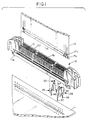
- Connector 10 is of a type of connector commonly called an "edge card” connector in that it has receptacle means in the form of a slot 12 (Fig. 3) for allowing insertion of a printed circuit card 13 into a contact area of the connector.
- the inserted printed circuit card has a mating edge 15 and a plurality of contact pads 17a, 17b adjacent the edge either on one or both sides of the board.
- Connector 10 is designed with terminals for engaging contact pads on both sides of the printed circuit board adjacent the edge thereof.
- Edge connectors such as connector 10 normally are elongated, as shown, and have rows of spring contact element receiving cavities generally designated 22, spaced along one or both sides of slot 12 lengthwise of a dielectric housing 16. As stated above, connector 10 has spring contact elements spaced along slot 12 on both sides thereof for engaging contact pads 17a, 17b on both sides of an inserted printed circuit card 13. It should be understood that the concepts of the invention are not limited to edge connectors of the character described, and the invention can be embodied in a wide variety of applicable electrical connectors.
- dielectric housing 16 includes a plurality of standoffs 18 (Figs. 1-2) depending from the housing for engaging a surface of printed circuit board 11. Often, the printed circuit board 11 is called a “mother board”, and the printed circuit card 13 which is inserted into slot 12 is called a “daughter board”. Dielectric housing 16 also includes a plurality of mounting or retention pegs 20 for locating connector 10 on mother board 11 by inserting the pegs into appropriate mounting holes 21 in the board.
- housing 16 includes a plurality of transverse cavities, generally designated 22, spaced longitudinally of slot 12 for receiving alternating differently configured terminals, as described hereinafter.
- Each cavity 22 has a cavity portion 22a on one side of slot 12 (the left-hand side as viewed in Figure 4) and a cavity portion 22b on the opposite side of the slot (the right-hand side as viewed in Figure 4).
- Cavities 22 are separated lengthwise of elongated housing 16 by walls or partitions which include wall portions 24a separating cavity portions 22a and wall portions 24b separating cavity portions 22b.
- cavity portions 22a and 22b are separated longitudinally of housing 16 by a center partition 23 at the bottom of cavity 22.
- housing 16 includes a plurality of recesses or holes 26a and 26b outside of cavity portions 22a and 22b, respectively, and generally in transverse alignment, for purposes described below.
- Each recess or hole 26a, 26b has a mouth 27 opening at the bottom of housing 16.
- the entire housing is unitarily molded of dielectric material such as plastic or the like.
- a plurality of terminals are mounted on housing 16, spaced longitudinally of the housing and corresponding to the plurality of transversely aligned cavity portions 22a, 22b and holes 26a, 26b.
- the printed circuit board i.e. the daughter board
- the mating edge which is inserted into the slot.
- One row of contact pads on each side of the board is located near the absolute edge of the board, and the other row of contact pads on each side of the board is spaced inwardly from the one row. Therefore, conventionally, terminals are located on housing 16 with contact elements alternating lengthwise of the housing for alternatingly engaging the contact pads in the two rows thereof along opposite sides of the mating edge of the printed circuit board.
- terminals are mounted on housing 16 in an alternating array lengthwise of the housing; there being an alternating array of terminals 28 and 30 on each opposite side of slot 12 (i.e., on each opposite side of the daughter board).
- terminals 28 alternate between adjacent terminals 30 lengthwise of slot 12 and on both sides of the slot.
- terminals 28 and 30 alternate transversely of the slot. As shown in Figure 1, each terminal 28 is aligned with a terminal 30 to create a pair of terminals, these terminals are then reversed with each alternating pair.
- Terminals 28 are signal terminals and are adapted for engaging contact pads 17a of signal circuit traces on the daughter board as well as signal terminal traces on mother board 11. As shown in Figure 1, contact pads 17a connected to the signal traces are adjacent edge 15 of edge card 13.
- each signal terminal 28 includes a body portion, generally designated 32, and a spring contact portion 34.
- Body portion 32 includes a base portion 36, a locking leg section 38 projecting upwardly from the base portion on the outside (relative to the card slot 12) of contact portion 34, and a mechanically non-functional section 40 projecting upwardly from the base portion on the inside (relative to the card slot) of contact portion 34.
- Locking leg section 38 is provided with barbs 42 whereby the locking leg can be press fit into a respective hole 26a for mounting terminal 28 on housing 16 by inserting locking leg 38 through mouth 27 of the respective hole 26a.
- Mechanically non-functional section 40 is provided in the form of a stub (as shown) connected to base portion 36 at a narrow area 44.
- a solder tail 46 projects downwardly from base portion 36 for insertion into a hole in mother board 11 and for electrical soldered interconnection with a signal trace either on the board or in a hole in the board. Such solder tail and mother board could be modified to permit surface mounting as is known in the industry.
- the spring contact portion 34 includes a resilient arm portion 35a and a mating portion 35b for engaging a contact pad 17a of a mating daughter board 13.
- the invention contemplates a method and a structure for tuning the impedance of electrical connector 10 which is interconnected in an electrical circuit having a given predetermined impedance.
- connector 10 being an edge connector
- the electrical circuit would be defined by the circuitry on the mother and daughter printed circuit boards.
- an ideal connector would be “transparent” so as to have as little affect on the circuit as possible. Therefore, the invention is directed to concepts for "tuning” or initially modifying the impedance of electrical connector 10 to match the given impedance of the interconnection system or the electrical circuit in which the connector is interconnected.
- the given impedance often is called the "characteristic" impedance of a circuit and usually is known.
- a manufacturer of electrical connectors often is provided by a customer with a characteristic impedance value of the circuit within which the customer is going to interconnect the particular connector.
- the customer typically desires a connector that will match the impedance of the circuit in order to minimize its affect on the circuit.
- the impedance of any circuit can be measured by various means, such as a time domain reflectometer which utilizes an electric analog to a radar system, as well as other measuring or analyzing devices.
- the impedance of any particular connector similarly can be measured in an input/output manner, again by using such instruments as the time domain reflectometer. If the impedance of the connector does not match the impedance of the interconnecting circuit, the present invention contemplates a method and structure for tuning or modifying the impedance of the connector during or prior to assembly thereof in order to substantially match the impedance of the circuit as closely as possible.
- a desired surface area for the stubs 40 can be calculated. Upon building prototypes to these dimensions, the exact desired area can then be determined by testing.
- the dies utilized for manufacturing the terminals 28 can be modified so as to trim or cut stubs 40 to the desired dimension. In fact, if desired, the entire stub 40 can be severed from terminal 28 by cutting the stub off at narrow area 44. In this manner, the entire area of signal terminals 28 can be varied by trimming stubs 40 whereupon the capacitance is varied.
- the connector can be "tuned" to the given impedance of the electrical circuit, as determined above.
- the dimension of such stubs 40 is thus set during the stamping process.
- the terminals 28, and likewise terminals 30, are inserted into housing 16 from the bottom in a manner known as "bottom-loading.”
- terminals 30 are ground terminals and are adapted for interconnection between ground circuit traces on the mother and daughter printed circuit boards.
- Each ground terminal 30 includes a body portion, generally designated 48, and a spring contact portion 50.
- Body portion 48 includes a base portion 52 having a locking leg 54 with barbs 42 for insertion upwardly through mouth 27 into hole 26b to mount the respective ground terminal on housing 16.
- Each ground terminal also includes an enlarged surface area portion 56 projecting upwardly from base portion 52 with an upstanding cantilevered portion 56b and terminating in spring contact portion 50.
- a solder tail 57 projects downwardly from base portion 52 for insertion into a hole in mother board 11 and for electrical soldered interconnection with a ground trace either on the board or in a hole in the board.
- the spring contact portion 50 includes a resilient arm portion 51 and a mating portion 51a for engaging a contact pad 17b of a mating daughter board 13.
- ground terminals 30 have significantly larger transverse areas than signal terminals 28. This can be seen by comparing the ground terminals in Figures 4 and 6 with the signal terminals in Figures 4 and 5. The significantly larger areas of the ground terminals are afforded by the enlarged surface area portions 56 of the ground terminals.
- the ground terminals effectively "shadow" the signal terminals and thereby provide increased electrical isolation, significantly reducing the crosstalk of connector 10 in a very simple and efficient manner.
- the ground terminal base 52, enlarged surface area 56 and spring contact resilient arm portion 51 have upstanding sides 52a, 56a and 51b, respectively, that define peripheral sides of a transverse area which is longitudinally aligned with and overlies the base 36 and spring contact resilient arm portion 35a of an adjacent signal terminal 28, as depicted in Figure 4.
- the invention also contemplates a structure for reducing the inductance of electrical connector 10, with the connector mounted to a mother board 11 wherein individual ground traces on the board all are part of a common ground circuit, as is found in many edge connectors. Therefore, it would be desirable to reduce the inductance through ground terminals 30 to the common ground circuit.
- each ground terminal 30 has a foot 60 for surface engaging a ground circuit trace on mother board 11.
- This additional foot and solder tail 57 are provided for engaging a common ground circuit on mother board 11.
- foot 60 is illustrated for surface mounting to the mother board, the foot could be a second solder tail for insertion into another hole in the printed circuit board.
- solder tails 46 and 57 for signal terminals 28 and ground terminals 30, respectively both could be feet for surface mounting to circuit traces on the printed circuit board.
- a larger contact surface area is provided for engaging the common ground circuit on the printed circuit board.
- the larger contact surface area reduces the voltage drop and reduces the inductance between a respective ground terminal and the common ground circuit on the printed circuit board.
- This structure improves the effectiveness of the ground terminals which is particularly important in achieving increased bandwidth and reducing ground bounce in high speed connectors.
- spring contact portions 34 of signal terminals 28 are located “deeper” within slot 12 than spring contact portions 50 of ground terminals 30. These differential locations enable the alternating terminals to engage two rows of contact pads on the daughter board, as described above. It can be seen that spring contact portions 34 and 50 extend transversely into slot 12. When the daughter printed circuit board 13 is inserted into the slot in the direction of arrow "A", the spring contact portions will be biased transversely outwardly while in engagement with the contact pads in two rows along the mating edge of the printed circuit board, the signal contact pads 17a being located nearer the absolute edge of the board than the ground contact pads 17b.
Landscapes
- Details Of Connecting Devices For Male And Female Coupling (AREA)
- Coupling Device And Connection With Printed Circuit (AREA)
Applications Claiming Priority (4)
| Application Number | Priority Date | Filing Date | Title |
|---|---|---|---|
| US900209 | 1992-06-17 | ||
| US07/900,209 US5259768A (en) | 1992-03-24 | 1992-06-17 | Impedance and inductance control in electrical connectors and including reduced crosstalk |
| EP98107143A EP0859433B1 (fr) | 1992-06-17 | 1993-06-08 | Contrôle d'impédance et d'inductance en connecteurs électriques à diaphonie réduite |
| EP93109181A EP0574805B1 (fr) | 1992-06-17 | 1993-06-08 | ContrÔle d'impédance et d'inductance dans connecteurs électriques à diaphonie réduite |
Related Parent Applications (1)
| Application Number | Title | Priority Date | Filing Date |
|---|---|---|---|
| EP98107143A Division EP0859433B1 (fr) | 1992-06-17 | 1993-06-08 | Contrôle d'impédance et d'inductance en connecteurs électriques à diaphonie réduite |
Publications (1)
| Publication Number | Publication Date |
|---|---|
| EP1261078A2 true EP1261078A2 (fr) | 2002-11-27 |
Family
ID=25412152
Family Applications (3)
| Application Number | Title | Priority Date | Filing Date |
|---|---|---|---|
| EP98107143A Expired - Lifetime EP0859433B1 (fr) | 1992-06-17 | 1993-06-08 | Contrôle d'impédance et d'inductance en connecteurs électriques à diaphonie réduite |
| EP93109181A Expired - Lifetime EP0574805B1 (fr) | 1992-06-17 | 1993-06-08 | ContrÔle d'impédance et d'inductance dans connecteurs électriques à diaphonie réduite |
| EP02018571A Withdrawn EP1261078A2 (fr) | 1992-06-17 | 1993-06-08 | Contrôle d' impédance et d' inductance dans des connecteurs électriques à diaphonie réduite |
Family Applications Before (2)
| Application Number | Title | Priority Date | Filing Date |
|---|---|---|---|
| EP98107143A Expired - Lifetime EP0859433B1 (fr) | 1992-06-17 | 1993-06-08 | Contrôle d'impédance et d'inductance en connecteurs électriques à diaphonie réduite |
| EP93109181A Expired - Lifetime EP0574805B1 (fr) | 1992-06-17 | 1993-06-08 | ContrÔle d'impédance et d'inductance dans connecteurs électriques à diaphonie réduite |
Country Status (9)
| Country | Link |
|---|---|
| US (1) | US5259768A (fr) |
| EP (3) | EP0859433B1 (fr) |
| JP (2) | JP2622929B2 (fr) |
| KR (1) | KR970003364B1 (fr) |
| DE (2) | DE69322208T2 (fr) |
| ES (1) | ES2124754T3 (fr) |
| MY (1) | MY106654A (fr) |
| SG (1) | SG46328A1 (fr) |
| TW (1) | TW215496B (fr) |
Cited By (4)
| Publication number | Priority date | Publication date | Assignee | Title |
|---|---|---|---|---|
| US7670196B2 (en) | 2006-08-02 | 2010-03-02 | Tyco Electronics Corporation | Electrical terminal having tactile feedback tip and electrical connector for use therewith |
| US7753742B2 (en) | 2006-08-02 | 2010-07-13 | Tyco Electronics Corporation | Electrical terminal having improved insertion characteristics and electrical connector for use therewith |
| US7789716B2 (en) | 2006-08-02 | 2010-09-07 | Tyco Electronics Corporation | Electrical connector having improved terminal configuration |
| US8142236B2 (en) | 2006-08-02 | 2012-03-27 | Tyco Electronics Corporation | Electrical connector having improved density and routing characteristics and related methods |
Families Citing this family (60)
| Publication number | Priority date | Publication date | Assignee | Title |
|---|---|---|---|---|
| JPH0631088U (ja) * | 1992-09-28 | 1994-04-22 | 日本エー・エム・ピー株式会社 | エッジコネクタ及びそれに使用する接触子 |
| US5503564A (en) * | 1992-10-30 | 1996-04-02 | The Whitaker Corporation | Assembly of an electrical connector and ejector unit for connecting IC cards to printed circuit boards |
| US5827075A (en) * | 1993-09-08 | 1998-10-27 | The Whitaker Corporation | Assembly of an electrical connector and ejector unit for connecting IC cards to printed circuit boards |
| JP2603158Y2 (ja) * | 1993-10-08 | 2000-02-28 | ヒロセ電機株式会社 | ラッチ付き回路基板用電気コネクタ |
| US7579269B2 (en) * | 1993-11-16 | 2009-08-25 | Formfactor, Inc. | Microelectronic spring contact elements |
| US6727580B1 (en) * | 1993-11-16 | 2004-04-27 | Formfactor, Inc. | Microelectronic spring contact elements |
| US5639266A (en) | 1994-01-11 | 1997-06-17 | Stewart Connector Systems, Inc. | High frequency electrical connector |
| US5791942A (en) * | 1994-01-11 | 1998-08-11 | Stewart Connector Systems, Inc. | High frequency electrical connector |
| US5496180A (en) * | 1994-04-06 | 1996-03-05 | The Whitaker Corporation | Surface mountable card edge connector |
| US5511985A (en) * | 1994-06-16 | 1996-04-30 | Burndy Corporation | Angled card edge connector |
| US5580257A (en) * | 1995-04-28 | 1996-12-03 | Molex Incorporated | High performance card edge connector |
| TW395069B (en) * | 1995-08-23 | 2000-06-21 | Connector Systems Tech Nv | Connector |
| US5749750A (en) * | 1995-08-23 | 1998-05-12 | Berg Technology, Inc. | Connector |
| US5895278A (en) * | 1996-10-10 | 1999-04-20 | Thomas & Betts Corporation | Controlled impedance, high density electrical connector |
| JP3424150B2 (ja) * | 1996-12-27 | 2003-07-07 | モレックス インコーポレーテッド | 電気コネクタ |
| US6067594A (en) * | 1997-09-26 | 2000-05-23 | Rambus, Inc. | High frequency bus system |
| US5876222A (en) * | 1997-11-07 | 1999-03-02 | Molex Incorporated | Electrical connector for printed circuit boards |
| WO1999041810A1 (fr) * | 1998-02-17 | 1999-08-19 | Rambus, Inc. | Connecteur muni de contacts a configuration alternee |
| US6439931B1 (en) | 1998-05-13 | 2002-08-27 | Molex Incorporated | Method and structure for tuning the impedance of electrical terminals |
| US6099328A (en) * | 1998-05-21 | 2000-08-08 | Molex Incorporated | High-speed edge connector |
| IL139807A0 (en) | 1998-06-02 | 2002-02-10 | Stewart Connector Systems Inc | High frequency electrical connector assembly such as multi-port multi-level connector assembly |
| US6095821A (en) * | 1998-07-22 | 2000-08-01 | Molex Incorporated | Card edge connector with improved reference terminals |
| US6015299A (en) | 1998-07-22 | 2000-01-18 | Molex Incorporated | Card edge connector with symmetrical board contacts |
| US6095872A (en) * | 1998-10-21 | 2000-08-01 | Molex Incorporated | Connector having terminals with improved soldier tails |
| CA2291373C (fr) | 1998-12-02 | 2002-08-06 | Nordx/Cdt, Inc. | Connecteurs modulaires a structures de compensation |
| US6254435B1 (en) | 1999-06-01 | 2001-07-03 | Molex Incorporated | Edge card connector for a printed circuit board |
| US6234807B1 (en) | 2000-01-24 | 2001-05-22 | International Business Machines Corporation | Circuit board connector edge with straddle pattern tab design for impedance-controlled connections |
| US6394823B1 (en) | 2000-05-26 | 2002-05-28 | Molex Incorporated | Connector with terminals having increased capacitance |
| US6506077B2 (en) | 2000-07-21 | 2003-01-14 | The Siemon Company | Shielded telecommunications connector |
| US6346010B1 (en) | 2000-08-10 | 2002-02-12 | The Wiremold Company | Modular connector |
| JP2003077564A (ja) * | 2001-08-31 | 2003-03-14 | Mitsumi Electric Co Ltd | メモリカード用コネクタ |
| US6811429B2 (en) * | 2001-08-31 | 2004-11-02 | International Business Machines Corporation | Low noise IDC terminal/pin arrangement for flat ribbon cable connectors |
| CN1870853B (zh) * | 2001-10-10 | 2012-01-18 | 莫莱克斯公司 | 高速差分信号边缘卡连接器电路板布局 |
| KR100444656B1 (ko) * | 2002-01-25 | 2004-08-21 | 주식회사 제일 | 반도체 테스트용 슬롯의 접촉장치 |
| KR100945283B1 (ko) * | 2002-10-15 | 2010-03-04 | 삼성전자주식회사 | Pcb |
| US7040934B2 (en) * | 2002-12-19 | 2006-05-09 | Intel Corporation | Add-in card to backplane connecting apparatus |
| JP2004265599A (ja) * | 2002-12-19 | 2004-09-24 | Iriso Denshi Kogyo Kk | 基板接続用コネクタ及びコネクタ接続用基板 |
| US6994563B2 (en) * | 2003-12-19 | 2006-02-07 | Lenovo (Singapore) Pte. Ltd. | Signal channel configuration providing increased capacitance at a card edge connection |
| JP4843263B2 (ja) * | 2005-06-14 | 2011-12-21 | 富士通コンポーネント株式会社 | フレキシブルプリントケーブル用コネクタ |
| JP4566076B2 (ja) * | 2005-06-29 | 2010-10-20 | タイコエレクトロニクスジャパン合同会社 | コネクタ |
| EP1791220A1 (fr) * | 2005-11-28 | 2007-05-30 | Hon Hai Precision Industry Co., Ltd. | Connecteur à grande fréquence pour carte imprimée |
| US7591655B2 (en) | 2006-08-02 | 2009-09-22 | Tyco Electronics Corporation | Electrical connector having improved electrical characteristics |
| JP5517287B2 (ja) | 2009-09-17 | 2014-06-11 | 矢崎総業株式会社 | インサート成形方法 |
| DE102009056171A1 (de) * | 2009-11-27 | 2011-06-16 | Ept Gmbh & Co. Kg | Steckverbinder für elektrische und elektronische Schaltelemente |
| CN201797097U (zh) * | 2010-05-21 | 2011-04-13 | 富士康(昆山)电脑接插件有限公司 | 一种电连接器及其导电端子 |
| US8215994B2 (en) * | 2010-10-18 | 2012-07-10 | Hon Hai Precision Ind. Co., Ltd. | Card edge connector having less resonance |
| WO2012138519A2 (fr) * | 2011-04-04 | 2012-10-11 | Fci | Connecteur électrique |
| US8419457B2 (en) * | 2011-08-26 | 2013-04-16 | Concraft Holding Co., Ltd. | Anti-electromagnetic interference electrical connector and terminal assembly thereof |
| US8696389B2 (en) * | 2011-09-30 | 2014-04-15 | Tyco Electronics Corporation | Card edge connector |
| US8517775B1 (en) * | 2012-02-13 | 2013-08-27 | Cheng Uei Precision Industry Co., Ltd. | Electrical connector |
| DE202012013323U1 (de) * | 2012-06-15 | 2016-04-17 | Yamaichi Electronics Deutschland Gmbh | Verbinder und Kontaktsystem |
| US9265152B2 (en) * | 2013-12-17 | 2016-02-16 | Lenovo Enterprise Solutions (Singapore) Pte. Ltd. | Dual side staggered surface mount dual in-line memory module |
| CN204966748U (zh) * | 2015-07-31 | 2016-01-13 | 富士康(昆山)电脑接插件有限公司 | 线缆连接器 |
| DE102016116127A1 (de) * | 2016-08-30 | 2018-03-01 | Dr. Ing. H.C. F. Porsche Aktiengesellschaft | Baukastensystem mit mehreren miteinander elektrisch verbindbaren Modulen |
| CN108963667B (zh) * | 2018-07-09 | 2020-07-24 | 肯上科技股份有限公司 | 高频连接器接地结构 |
| CN109586065A (zh) * | 2018-12-03 | 2019-04-05 | 番禺得意精密电子工业有限公司 | 电连接器 |
| JP7314556B2 (ja) * | 2019-03-22 | 2023-07-26 | 京セラドキュメントソリューションズ株式会社 | コネクター |
| WO2021059970A1 (fr) * | 2019-09-24 | 2021-04-01 | 株式会社村田製作所 | Connecteur électrique et ensemble connecteur électrique |
| US11296464B2 (en) * | 2020-02-14 | 2022-04-05 | TE Connectivity Services Gmbh | Impedance control connector |
| JP7467236B2 (ja) * | 2020-05-28 | 2024-04-15 | 日本航空電子工業株式会社 | フローティングコネクタ |
Family Cites Families (20)
| Publication number | Priority date | Publication date | Assignee | Title |
|---|---|---|---|---|
| US3196377A (en) * | 1961-08-04 | 1965-07-20 | Matrix Science Corp | Electrical connector |
| US3539976A (en) * | 1968-01-04 | 1970-11-10 | Amp Inc | Coaxial connector with controlled characteristic impedance |
| US3470522A (en) * | 1968-02-26 | 1969-09-30 | Bunker Ramo | Electrical connector |
| US3573704A (en) * | 1969-06-23 | 1971-04-06 | Gen Electric | Flatline cable impedance matching adapter |
| JPS5819884A (ja) * | 1981-07-29 | 1983-02-05 | 日本航空電子工業株式会社 | 高密度圧接型コネクタ |
| US4419626A (en) * | 1981-08-25 | 1983-12-06 | Daymarc Corporation | Broad band contactor assembly for testing integrated circuit devices |
| US4461522A (en) * | 1982-08-23 | 1984-07-24 | Amp Incorporated | Zero insertion force connector for a circuit board |
| US4552420A (en) * | 1983-12-02 | 1985-11-12 | E. I. Du Pont De Nemours And Company | Electrical connector using a flexible circuit having an impedance control arrangement thereon |
| US4707039A (en) * | 1984-04-11 | 1987-11-17 | John Fluke Mfg. Co., Inc. | Coaxial connector for controlled impedance transmission lines |
| FR2619472B1 (fr) * | 1987-08-14 | 1992-01-24 | Drogo Pierre | Douille de reception d'une broche pour realiser une connexion electrique et connecteur electrique comportant au moins une telle douille |
| US4917616A (en) * | 1988-07-15 | 1990-04-17 | Amp Incorporated | Backplane signal connector with controlled impedance |
| US5060373A (en) * | 1989-08-22 | 1991-10-29 | The Phoenix Company Of Chicago, Inc. | Methods for making coaxial connectors |
| US5051099A (en) * | 1990-01-10 | 1991-09-24 | Amp Incorporated | High speed card edge connector |
| US5026292A (en) * | 1990-01-10 | 1991-06-25 | Amp Incorporated | Card edge connector |
| US5071371A (en) * | 1990-03-30 | 1991-12-10 | Molex Incorporated | Electrical card edge connector assembly |
| US5024609A (en) * | 1990-04-04 | 1991-06-18 | Burndy Corporation | High-density bi-level card edge connector and method of making the same |
| JP2952690B2 (ja) * | 1990-07-23 | 1999-09-27 | 日本エー・エム・ピー株式会社 | 高周波コネクタ |
| US5082459A (en) * | 1990-08-23 | 1992-01-21 | Amp Incorporated | Dual readout simm socket |
| JPH0455764U (fr) * | 1990-09-21 | 1992-05-13 | ||
| JP2587316B2 (ja) * | 1990-10-08 | 1997-03-05 | 第一電子工業株式会社 | 同軸フラットケーブル用多極電気コネクタ |
-
1992
- 1992-06-17 US US07/900,209 patent/US5259768A/en not_active Expired - Lifetime
-
1993
- 1993-04-06 MY MYPI93000617A patent/MY106654A/en unknown
- 1993-04-20 TW TW082103029A patent/TW215496B/zh active
- 1993-05-11 JP JP5132871A patent/JP2622929B2/ja not_active Expired - Fee Related
- 1993-06-08 EP EP98107143A patent/EP0859433B1/fr not_active Expired - Lifetime
- 1993-06-08 DE DE69322208T patent/DE69322208T2/de not_active Expired - Fee Related
- 1993-06-08 EP EP93109181A patent/EP0574805B1/fr not_active Expired - Lifetime
- 1993-06-08 ES ES93109181T patent/ES2124754T3/es not_active Expired - Lifetime
- 1993-06-08 SG SG1996002999A patent/SG46328A1/en unknown
- 1993-06-08 DE DE69332768T patent/DE69332768T2/de not_active Expired - Fee Related
- 1993-06-08 EP EP02018571A patent/EP1261078A2/fr not_active Withdrawn
- 1993-06-16 KR KR1019930010944A patent/KR970003364B1/ko not_active IP Right Cessation
-
1996
- 1996-04-05 JP JP1996003651U patent/JP3032913U/ja not_active Expired - Lifetime
Cited By (4)
| Publication number | Priority date | Publication date | Assignee | Title |
|---|---|---|---|---|
| US7670196B2 (en) | 2006-08-02 | 2010-03-02 | Tyco Electronics Corporation | Electrical terminal having tactile feedback tip and electrical connector for use therewith |
| US7753742B2 (en) | 2006-08-02 | 2010-07-13 | Tyco Electronics Corporation | Electrical terminal having improved insertion characteristics and electrical connector for use therewith |
| US7789716B2 (en) | 2006-08-02 | 2010-09-07 | Tyco Electronics Corporation | Electrical connector having improved terminal configuration |
| US8142236B2 (en) | 2006-08-02 | 2012-03-27 | Tyco Electronics Corporation | Electrical connector having improved density and routing characteristics and related methods |
Also Published As
| Publication number | Publication date |
|---|---|
| TW215496B (en) | 1993-11-01 |
| DE69322208T2 (de) | 1999-08-05 |
| EP0859433A2 (fr) | 1998-08-19 |
| MY106654A (en) | 1995-07-31 |
| JP2622929B2 (ja) | 1997-06-25 |
| JPH0636837A (ja) | 1994-02-10 |
| US5259768A (en) | 1993-11-09 |
| DE69332768T2 (de) | 2004-02-05 |
| SG46328A1 (en) | 1998-02-20 |
| EP0574805A2 (fr) | 1993-12-22 |
| ES2124754T3 (es) | 1999-02-16 |
| EP0574805A3 (fr) | 1995-04-12 |
| KR970003364B1 (ko) | 1997-03-17 |
| EP0859433A3 (fr) | 1999-09-29 |
| DE69332768D1 (de) | 2003-04-17 |
| JP3032913U (ja) | 1997-01-17 |
| EP0574805B1 (fr) | 1998-11-25 |
| EP0859433B1 (fr) | 2003-03-12 |
| DE69322208D1 (de) | 1999-01-07 |
| KR940001492A (ko) | 1994-01-11 |
Similar Documents
| Publication | Publication Date | Title |
|---|---|---|
| EP0859433B1 (fr) | Contrôle d'impédance et d'inductance en connecteurs électriques à diaphonie réduite | |
| US5853303A (en) | Impedance and inductance control in electrical connectors and including reduced crosstalk | |
| US5309630A (en) | Impedance and inductance control in electrical connectors | |
| US5921815A (en) | Impedance and inductance control in electrical connectors | |
| US4326765A (en) | Electronic device carrier | |
| US5664968A (en) | Connector assembly with shielded modules | |
| US6425766B1 (en) | Impedance control in edge card connector systems | |
| KR940002006B1 (ko) | 전기 코넥터의 신호보전용 기준도체 | |
| WO2001093375A2 (fr) | Connecteur dote de terminaux a capacite accrue | |
| US6648657B1 (en) | Electrical connector having ground buses | |
| US5409406A (en) | Connector for high density electronic assemblies | |
| US5709573A (en) | Connector for high density electronic assemblies | |
| US6398580B2 (en) | Electrical terminal member | |
| US6645009B1 (en) | High density electrical connector with lead-in device | |
| EP0562427B1 (fr) | ContrÔle d'impédance et inductance pour des connecteurs électriques | |
| US6123584A (en) | Connector | |
| US6802732B1 (en) | Card edge connector | |
| EP0342873B1 (fr) | Connecteur pour le montage sur une surface | |
| US5921812A (en) | System for mounting two connectors on two sides of board | |
| US5580267A (en) | Electrical connector for a printed circuit board | |
| JPH06325828A (ja) | プラグコネクタ |
Legal Events
| Date | Code | Title | Description |
|---|---|---|---|
| PUAI | Public reference made under article 153(3) epc to a published international application that has entered the european phase |
Free format text: ORIGINAL CODE: 0009012 |
|
| 17P | Request for examination filed |
Effective date: 20020816 |
|
| AC | Divisional application: reference to earlier application |
Ref document number: 859433 Country of ref document: EP Ref document number: 574805 Country of ref document: EP |
|
| AK | Designated contracting states |
Kind code of ref document: A2 Designated state(s): DE ES FR GB IT NL |
|
| RIN1 | Information on inventor provided before grant (corrected) |
Inventor name: SCHEER, DENNIS S. Inventor name: HARWARTH, FRANK A. Inventor name: BRUNKER, DAVID L. |
|
| STAA | Information on the status of an ep patent application or granted ep patent |
Free format text: STATUS: THE APPLICATION HAS BEEN WITHDRAWN |
|
| 18W | Application withdrawn |
Effective date: 20050221 |