EP1256975A2 - Vertical type wafer supporting jig - Google Patents
Vertical type wafer supporting jig Download PDFInfo
- Publication number
- EP1256975A2 EP1256975A2 EP02010097A EP02010097A EP1256975A2 EP 1256975 A2 EP1256975 A2 EP 1256975A2 EP 02010097 A EP02010097 A EP 02010097A EP 02010097 A EP02010097 A EP 02010097A EP 1256975 A2 EP1256975 A2 EP 1256975A2
- Authority
- EP
- European Patent Office
- Prior art keywords
- support
- support plates
- vertical type
- wafer supporting
- pillars
- Prior art date
- Legal status (The legal status is an assumption and is not a legal conclusion. Google has not performed a legal analysis and makes no representation as to the accuracy of the status listed.)
- Granted
Links
Images



Classifications
-
- H—ELECTRICITY
- H10—SEMICONDUCTOR DEVICES; ELECTRIC SOLID-STATE DEVICES NOT OTHERWISE PROVIDED FOR
- H10P—GENERIC PROCESSES OR APPARATUS FOR THE MANUFACTURE OR TREATMENT OF DEVICES COVERED BY CLASS H10
- H10P72/00—Handling or holding of wafers, substrates or devices during manufacture or treatment thereof
- H10P72/10—Handling or holding of wafers, substrates or devices during manufacture or treatment thereof using carriers specially adapted therefor, e.g. front opening unified pods [FOUP]
- H10P72/12—Vertical boat type carrier whereby the substrates are horizontally supported, e.g. comprising rod-shaped elements
-
- C—CHEMISTRY; METALLURGY
- C30—CRYSTAL GROWTH
- C30B—SINGLE-CRYSTAL GROWTH; UNIDIRECTIONAL SOLIDIFICATION OF EUTECTIC MATERIAL OR UNIDIRECTIONAL DEMIXING OF EUTECTOID MATERIAL; REFINING BY ZONE-MELTING OF MATERIAL; PRODUCTION OF A HOMOGENEOUS POLYCRYSTALLINE MATERIAL WITH DEFINED STRUCTURE; SINGLE CRYSTALS OR HOMOGENEOUS POLYCRYSTALLINE MATERIAL WITH DEFINED STRUCTURE; AFTER-TREATMENT OF SINGLE CRYSTALS OR A HOMOGENEOUS POLYCRYSTALLINE MATERIAL WITH DEFINED STRUCTURE; APPARATUS THEREFOR
- C30B31/00—Diffusion or doping processes for single crystals or homogeneous polycrystalline material with defined structure; Apparatus therefor
- C30B31/06—Diffusion or doping processes for single crystals or homogeneous polycrystalline material with defined structure; Apparatus therefor by contacting with diffusion material in the gaseous state
- C30B31/14—Substrate holders or susceptors
-
- H—ELECTRICITY
- H10—SEMICONDUCTOR DEVICES; ELECTRIC SOLID-STATE DEVICES NOT OTHERWISE PROVIDED FOR
- H10P—GENERIC PROCESSES OR APPARATUS FOR THE MANUFACTURE OR TREATMENT OF DEVICES COVERED BY CLASS H10
- H10P72/00—Handling or holding of wafers, substrates or devices during manufacture or treatment thereof
- H10P72/10—Handling or holding of wafers, substrates or devices during manufacture or treatment thereof using carriers specially adapted therefor, e.g. front opening unified pods [FOUP]
- H10P72/12—Vertical boat type carrier whereby the substrates are horizontally supported, e.g. comprising rod-shaped elements
- H10P72/127—Vertical boat type carrier whereby the substrates are horizontally supported, e.g. comprising rod-shaped elements characterised by the substrate support
Definitions
- the present invention relates to a vertical type wafer supporting jig for support of a plurality of wafers onto many support plates stacked superposed on one another with a predetermined wafer mounting space being provided therebetween, whereby the support plates are fixed to a plurality of support pillars extending in a vertical direction.
- Semiconductor supporting jigs are used for holding many semiconductor wafers aligned, and particularly, vertical type wafer supporting jigs are suitable for a so-called wafer supporting boat for use in transporting wafers into and out of a wafer heat treatment apparatus.
- a wafer treatment apparatus for performing drive-in treatment comprising placing semiconductor wafers (which is sometimes referred to simply as "wafers") inside a heating furnace surrounded by a heater, and allowing impurities to permeate inside the wafer by heating under a high temperature atmosphere in a temperature range of from about 400 to 1400 °C while flowing gaseous raw material together with a predetermined carrier gas
- cassette boats for supporting the wafers aligned and mother boat or a wafer support boats (supporting jigs) for mounting thereon a plurality of said cassette boats are denoted collectively as wafer supporting jigs.
- the wafer supporting jigs are suitable for handling a plurality of thus supported wafers in one unit in each process step, and, in general, processing of the wafers is performed together with the wafer supporting jig, for instance, in the heat treatment step as described above, or in a cleaning step using, for example, hydrofluoric acid as the cleaning liquid.
- the material for the wafer supporting jigs is quartz glass, silicon, or compounds thereof.
- the vertical type wafer supporting jig 10 shown in Fig. 7 and Fig. 8 comprises a top plate 12 and a bottom plate 14 on the upper and the lower ends thereof, and a plurality (i.e., four, in the example shown in the figure) of support pillars 16a to 16d are attached thereto by welding.
- a number of ring-like support plates 18 corresponding to the number of the wafers to be placed in the apparatus are attached, by welding, to the plurality of support pillars 16a to 16d arranged in the vertical direction and set apart exactly from each other.
- a plurality (e.g., 3 pieces) of wafer supporting protrusions 20 are provided on the upper plane of said ring-like supporting plate 18 by taking proper distance from each other, and the wafers W are mounted on the support plate 18 via the wafer supporting protrusions 20.
- the vertical type wafer supporting jig 10 of a conventional type care should be made by taking the size of the wafers W to be handled; for instance, the bottom plate 14 of each of the supporting member inside each of the wafer supporting jig is taken as the standard, and the position set at a distance from the standard plane for attaching each of the supporting plates should be set within the dimensional allowance, or the top plate 12 and the bottom plate 14 should be held within the axial degree allowance, i.e., the allowance in tilting degree with respect to the central axis, etc.
- the size of the rings at present are, for instance, 2 to 3 mm in thickness t, 170 to 180 mm in aperture D, and the dimensional allowance in the position for their attachment in the longitudinal direction of the boat of each ring as taken from the standard plane is within ⁇ 0.2 mm, and such dimensional ratio and the requirement on the precision may increase but never decrease.
- the wafer supporting jigs 10 in use are handled in units with wafers and are subjected to various types of treatments, they are under danger of suffering from thermal deformation, a change with passage of time due to degradation, melting, wear damage, etc., attributed to the use of cleaning solution on cleaning treatment, or to breakage due to careless operator.
- Wafer supporting jigs 10 are made from an expensive material having high chemical stability, and in case even one support plate should require replacement among the many support plates (e.g., 50 wafer support plates per single wafer supporting jig) constituting the unit, the welded old support plates should be cut off and removed by using a cutter and the like, and then a new one should be heated for welding. Such a repair treatment is not easily afforded from technical and economical viewpoint, because it may impair the precision of attachment of the constituting support members around the replaced one.
- the support plates that are used in wafer support jigs frequently subjected to heat treatment tend to cause deformation at higher rates as compared with wafer support jigs used in other processes.
- the wafer supporting jig should be newly fabricated at a large expense.
- the problems of the vertical type wafer supporting jig 10 above are, that there is difficulty in carrying out the welding work while retaining dimensional precision of each member due to the working on fabrication; and, since the support plate 18 is relatively thin with respect to its planar size because the thickness thereof is determined in correspondence with the wafer, that the welding requires high skill because the portions other than the welding position are subject to thermal deformation on welding the support plates to the pillars 16a to 16d. Furthermore, in the repair working, there is fear of causing defects on the surrounding sound support plates 18 on repairing the defective support plate 18 by welding or by thermal treatment. Accordingly, there are other problems as such that a highly skilled technique is required for the repair, that the repair cost becomes costly, etc.
- the present invention has been made with an aim to further improve the above methods for fixing the support plates.
- the present invention provides a vertical type wafer supporting jig which does not employ the conventional welding means for fixing the ring-like support plates to the pillars, which enables fixing the support plates by a simple structure that surely preventing the falling off of the ring-like support plates from occurring, and which also is capable of rapidly cope with the demand of repair.
- support groove portions for inserting and supporting the support plates are formed in the support pillars with a predetermined interval between them, a fixing rod is provided extending along at least one of the support pillars, whereby in a peripheral part of the support plates at least one receiving groove is provided, said receiving groove is provided to receive and to engage the fixing rod, and the support plates are secured in engagement with and supported by the support pillars by causing each of the support plates to be inserted into and supported by the support groove portions and causing the fixing rod to be received in the at least one receiving groove of each of the support plates.
- the vertical type wafer supporting jig By using the vertical type wafer supporting jig according to the present invention, there is no need of welding the support plates during the assembly process of the wafer supporting jig as required in the conventional technique, and thereby the wafer supporting jig can be completed by a simple assembly; hence, there is no fear of impairing the dimensional precision or of requiring high skill not only on assemblage but also on repair.
- the single support plate that is produced under strict quality control itself assures the quality of the wafer supporting jig.
- the repair can be completed by a simple exchange of the support plate, the repair can be rapidly accomplished without impairing the other sound support plates, and a repair service of high quality can be provided at a low cost and yet, without impairing the function of the wafer supporting jig.
- two fixing rods are provided adjacent to two support pillars on the side of inserting the support plates of the plural support pillars above, and by further providing two receiving grooves to the peripheral parts of said support plates in correspondence to said fixing rods in such a manner that said support plates can be inserted to the support groove portions and held thereby and causing the two fixing rods to be fitted to the two receiving grooves of the corresponding support plates so as for the support plate to be fixed to and supported by the support pillars, the inserted support plates can be advantageously supported and fixed surely by the two support pillars.
- a constitution of the wafer supporting jig 10a according to the present invention is basically the same as the prior art constitution shown in Figs. 7 and 8. Hence, in Figs. 1 to 6, the members that are the same as or similar to those shown in Figs. 7 and 8 are described by referring with the same symbols.
- the constitution of the vertical type wafer supporting jig 10a according to the present invention is similar to a conventional vertical type wafer supporting jig 10 in that many wafers W are mounted via wafer-support protrusions 20 onto a plurality of ring-like support plates 18 stacked superposed on one another and fixed in a vertical direction to a plurality of support pillars (4 support pillars in the illustrated example) 16a to 16d with a predetermined wafer mounting interval being provided among them.
- the key of the vertical type wafer supporting jig 10a according to the present invention is that, differing from the conventional constitution of the ring-like support plates 18 being fixed to the support pillars 16a to 16d by welding, a novel constitution as described hereinafter is employed to fix the support pillars 16a to 16d without employing welding.
- support groove portions 22 for inserting and sustaining therein the support plates 18 are perforated with a predetermined interval taken on the upper and the lower directions thereof (Fig. 6). Furthermore, a fixing rod 24 adjacent to at least one of the support pillars 16a to 16d is connected by a means such as welding to the side plane of the support pillars 16a to 16d via a connecting portion 26.
- the fixing rod 24 is preferably formed into a round rod having a small diameter.
- the fixing rod 24 is preferably provided in such a manner that fixing rods 24 and 24 are each formed adjacent to two support pillars 16a and 16d, respectively, which are, among the support pillars 16a to 16d, in the side of inserting the support plate 18.
- At least one receiving groove 28 is perforated in the periphery of the ring-like support plate 18 in correspondence with the fixing rod 24.
- the receiving groove 28 it is preferred that two receiving grooves 28 and 28 are provided in correspondence with the two fixing rods 24 and 24 described above.
- the support plate 18 can be supported and fixed by said support pillars 16a to 16d, such that the support plate 18 is inserted and held with the support groove portion 22, while the fixing rods 24 and 24 are fitted in the receiving grooves 28 and 28 of the supporting plate 18. If the support plate 18 should be simply inserted into the support groove portion 22, the support plate 18 remains unstable and would easily fall off, but by fitting the fixing rod 24 into the receiving groove 28 at the same time, the support plate 18 would be firmly fixed to completely eliminate the fear of causing falling off.
- the vertical type wafer supporting jig according to the present invention provides a great effect as such in which a ring-like support plate can be fixed to support pillars by a simple structure without adopting conventional welding means as fixing means and the ring-like support plate can be surely prevented from falling off, and which can rapidly cope with a demand for repair.
Landscapes
- Chemical & Material Sciences (AREA)
- Engineering & Computer Science (AREA)
- Crystallography & Structural Chemistry (AREA)
- Materials Engineering (AREA)
- Metallurgy (AREA)
- Organic Chemistry (AREA)
- Container, Conveyance, Adherence, Positioning, Of Wafer (AREA)
Abstract
Description
- The present invention relates to a vertical type wafer supporting jig for support of a plurality of wafers onto many support plates stacked superposed on one another with a predetermined wafer mounting space being provided therebetween, whereby the support plates are fixed to a plurality of support pillars extending in a vertical direction.
- Semiconductor supporting jigs are used for holding many semiconductor wafers aligned, and particularly, vertical type wafer supporting jigs are suitable for a so-called wafer supporting boat for use in transporting wafers into and out of a wafer heat treatment apparatus.
- In a semiconductor production process in which is used a wafer treatment apparatus for performing drive-in treatment comprising placing semiconductor wafers (which is sometimes referred to simply as "wafers") inside a heating furnace surrounded by a heater, and allowing impurities to permeate inside the wafer by heating under a high temperature atmosphere in a temperature range of from about 400 to 1400 °C while flowing gaseous raw material together with a predetermined carrier gas, conventionally used are cassette boats for supporting the wafers aligned and mother boat or a wafer support boats (supporting jigs) for mounting thereon a plurality of said cassette boats, and these are denoted collectively as wafer supporting jigs.
- The wafer supporting jigs are suitable for handling a plurality of thus supported wafers in one unit in each process step, and, in general, processing of the wafers is performed together with the wafer supporting jig, for instance, in the heat treatment step as described above, or in a cleaning step using, for example, hydrofluoric acid as the cleaning liquid. Thus, by taking chemical stability and heat resistance into consideration, generally used as the material for the wafer supporting jigs is quartz glass, silicon, or compounds thereof.
- For instance, the vertical type
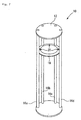
wafer supporting jig 10 shown in Fig. 7 and Fig. 8 comprises atop plate 12 and abottom plate 14 on the upper and the lower ends thereof, and a plurality (i.e., four, in the example shown in the figure) ofsupport pillars 16a to 16d are attached thereto by welding. A number of ring-like support plates 18 corresponding to the number of the wafers to be placed in the apparatus are attached, by welding, to the plurality ofsupport pillars 16a to 16d arranged in the vertical direction and set apart exactly from each other. A plurality (e.g., 3 pieces) ofwafer supporting protrusions 20 are provided on the upper plane of said ring-like supportingplate 18 by taking proper distance from each other, and the wafers W are mounted on thesupport plate 18 via thewafer supporting protrusions 20. - However, in producing the vertical type
wafer supporting jig 10 of a conventional type, care should be made by taking the size of the wafers W to be handled; for instance, thebottom plate 14 of each of the supporting member inside each of the wafer supporting jig is taken as the standard, and the position set at a distance from the standard plane for attaching each of the supporting plates should be set within the dimensional allowance, or thetop plate 12 and thebottom plate 14 should be held within the axial degree allowance, i.e., the allowance in tilting degree with respect to the central axis, etc. - The size of the rings at present are, for instance, 2 to 3 mm in thickness t, 170 to 180 mm in aperture D, and the dimensional allowance in the position for their attachment in the longitudinal direction of the boat of each ring as taken from the standard plane is within ± 0.2 mm, and such dimensional ratio and the requirement on the precision may increase but never decrease.
- Furthermore, since the
wafer supporting jigs 10 in use are handled in units with wafers and are subjected to various types of treatments, they are under danger of suffering from thermal deformation, a change with passage of time due to degradation, melting, wear damage, etc., attributed to the use of cleaning solution on cleaning treatment, or to breakage due to careless operator. -
Wafer supporting jigs 10 are made from an expensive material having high chemical stability, and in case even one support plate should require replacement among the many support plates (e.g., 50 wafer support plates per single wafer supporting jig) constituting the unit, the welded old support plates should be cut off and removed by using a cutter and the like, and then a new one should be heated for welding. Such a repair treatment is not easily afforded from technical and economical viewpoint, because it may impair the precision of attachment of the constituting support members around the replaced one. - In particular, the support plates that are used in wafer support jigs frequently subjected to heat treatment tend to cause deformation at higher rates as compared with wafer support jigs used in other processes. In case of a defect attributed not only to a single support member, and requires replacement of plural support plates or repair of the deformed member, the wafer supporting jig should be newly fabricated at a large expense.
- Accordingly, the problems of the vertical type
wafer supporting jig 10 above are, that there is difficulty in carrying out the welding work while retaining dimensional precision of each member due to the working on fabrication; and, since thesupport plate 18 is relatively thin with respect to its planar size because the thickness thereof is determined in correspondence with the wafer, that the welding requires high skill because the portions other than the welding position are subject to thermal deformation on welding the support plates to thepillars 16a to 16d. Furthermore, in the repair working, there is fear of causing defects on the surroundingsound support plates 18 on repairing thedefective support plate 18 by welding or by thermal treatment. Accordingly, there are other problems as such that a highly skilled technique is required for the repair, that the repair cost becomes costly, etc. - In the light of the aforementioned disadvantages of the prior art technology, there have been proposed a vertical type wafer enclosing jig (Japanese Utility Model Laid-Open No. 45332/1994) or a heat treatment board (unexamined published Japanese patent Laid-Open 237781/1997) employing a non-welding method for fixing the support plates. However, although these proposed methods for fixing the support plates are improved in that they to not use welding, they still had do be simplified in operations for fixing the support plates.
- The present invention has been made with an aim to further improve the above methods for fixing the support plates. The present invention provides a vertical type wafer supporting jig which does not employ the conventional welding means for fixing the ring-like support plates to the pillars, which enables fixing the support plates by a simple structure that surely preventing the falling off of the ring-like support plates from occurring, and which also is capable of rapidly cope with the demand of repair.
- In order to solve the above problems of generic vertical type wafer supporting jig, it is suggested by the present invention that support groove portions for inserting and supporting the support plates are formed in the support pillars with a predetermined interval between them, a fixing rod is provided extending along at least one of the support pillars, whereby in a peripheral part of the support plates at least one receiving groove is provided, said receiving groove is provided to receive and to engage the fixing rod, and the support plates are secured in engagement with and supported by the support pillars by causing each of the support plates to be inserted into and supported by the support groove portions and causing the fixing rod to be received in the at least one receiving groove of each of the support plates.
- By using the vertical type wafer supporting jig according to the present invention, there is no need of welding the support plates during the assembly process of the wafer supporting jig as required in the conventional technique, and thereby the wafer supporting jig can be completed by a simple assembly; hence, there is no fear of impairing the dimensional precision or of requiring high skill not only on assemblage but also on repair. In particular, the single support plate that is produced under strict quality control itself assures the quality of the wafer supporting jig. Further, the repair can be completed by a simple exchange of the support plate, the repair can be rapidly accomplished without impairing the other sound support plates, and a repair service of high quality can be provided at a low cost and yet, without impairing the function of the wafer supporting jig.
- Preferably, two fixing rods are provided adjacent to two support pillars on the side of inserting the support plates of the plural support pillars above, and by further providing two receiving grooves to the peripheral parts of said support plates in correspondence to said fixing rods in such a manner that said support plates can be inserted to the support groove portions and held thereby and causing the two fixing rods to be fitted to the two receiving grooves of the corresponding support plates so as for the support plate to be fixed to and supported by the support pillars, the inserted support plates can be advantageously supported and fixed surely by the two support pillars.
- An embodiment according to the present invention is described below based on the attached Figs. 1 to 6. However, it should be understood that the case shown in the figures are provided only as examples, and that various modifications can be made thereto so long as they do not deviate from the technical concept of the present invention.
-
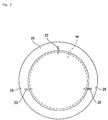
- Fig. 1 is a partially sectioned plan view showing a main part of a vertical type wafer supporting jig of the present invention.
- Fig. 2 is a plan view showing a support plate in the vertical type wafer supporting jig of the present invention.
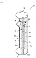
- Fig. 3 is a perspective view showing a state that one support plate is inserted and fixed to the vertical type wafer supporting jig of the present invention.
- Fig. 4 is a perspective view showing a state that the vertical type wafer supporting jig of the present invention is rotated by 90° from the state of Fig. 3.
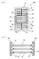
- Fig. 5 is a partially cutaway side whole view showing the vertical type wafer supporting jig of the present invention.
- Fig. 6 is a sectional explanatory view showing a main part of the vertical type wafer supporting jig of the present invention.
- Fig. 7 is a perspective view showing a state that one support plate is welded to a conventional vertical type wafer supporting jig.
- Fig. 8 is a partially cutaway side whole view showing the conventional vertical type wafer supporting jig.
-
- A constitution of the
wafer supporting jig 10a according to the present invention is basically the same as the prior art constitution shown in Figs. 7 and 8. Hence, in Figs. 1 to 6, the members that are the same as or similar to those shown in Figs. 7 and 8 are described by referring with the same symbols. - The constitution of the vertical type
wafer supporting jig 10a according to the present invention is similar to a conventional vertical typewafer supporting jig 10 in that many wafers W are mounted via wafer-support protrusions 20 onto a plurality of ring-like support plates 18 stacked superposed on one another and fixed in a vertical direction to a plurality of support pillars (4 support pillars in the illustrated example) 16a to 16d with a predetermined wafer mounting interval being provided among them. - The key of the vertical type
wafer supporting jig 10a according to the present invention is that, differing from the conventional constitution of the ring-like support plates 18 being fixed to thesupport pillars 16a to 16d by welding, a novel constitution as described hereinafter is employed to fix thesupport pillars 16a to 16d without employing welding. - In the
support pillars 16a to 16d of the vertical typewafer supporting jig 10a according to the present invention, supportgroove portions 22 for inserting and sustaining therein thesupport plates 18 are perforated with a predetermined interval taken on the upper and the lower directions thereof (Fig. 6). Furthermore, afixing rod 24 adjacent to at least one of thesupport pillars 16a to 16d is connected by a means such as welding to the side plane of thesupport pillars 16a to 16d via a connectingportion 26. Thefixing rod 24 is preferably formed into a round rod having a small diameter. Thefixing rod 24 is preferably provided in such a manner that fixingrods support pillars support pillars 16a to 16d, in the side of inserting thesupport plate 18. - On the other hand, at least one receiving
groove 28 is perforated in the periphery of the ring-like support plate 18 in correspondence with thefixing rod 24. As the receivinggroove 28, it is preferred that two receivinggrooves fixing rods - By using such a constitution above, the
support plate 18 can be supported and fixed by saidsupport pillars 16a to 16d, such that thesupport plate 18 is inserted and held with thesupport groove portion 22, while thefixing rods receiving grooves plate 18. If thesupport plate 18 should be simply inserted into thesupport groove portion 22, thesupport plate 18 remains unstable and would easily fall off, but by fitting thefixing rod 24 into thereceiving groove 28 at the same time, thesupport plate 18 would be firmly fixed to completely eliminate the fear of causing falling off. - As described above, the vertical type wafer supporting jig according to the present invention provides a great effect as such in which a ring-like support plate can be fixed to support pillars by a simple structure without adopting conventional welding means as fixing means and the ring-like support plate can be surely prevented from falling off, and which can rapidly cope with a demand for repair.
-
- 10:
- conventional vertical type wafer supporting jig,
- 10a:
- vertical type wafer supporting jig of the present invention,
- 12:
- top plate,
- 14:
- bottom plate,
- 16a - 16d:
- support pillar,
- 18:
- ring-like support plate,
- 20:
- wafer supporting protrusion,
- 22:
- support groove portion,
- 24:
- fixing rod,
- 26:
- connecting portion,
- 28:
- receiving groove, W: wafer.
Claims (6)
- A vertical type wafer supporting jig for support of a plurality of wafers onto many support plates stacked superposed on one another with a predetermined wafer mounting space being provided therebetween, whereby the support plates are fixed to a plurality of support pillars extending in a vertical direction, characterized in that support groove portions for inserting and supporting the support plates are formed in the support pillars with a predetermined interval between them, a fixing rod is provided extending along at least one of the support pillars, whereby in a peripheral part of the support plates at least one receiving groove is provided, said receiving groove is provided to receive and to engage the fixing rod, and the support plates are secured in engagement with and supported by the support pillars by causing each of the support plates to be inserted into and supported by the support groove portions and causing the fixing rod to be received in the at least one receiving groove of each of the support plates.
- A vertical type wafer supporting jig as set forth in claim 1, characterized in that the least one fixing rod extends adjacent one of the support pillars.
- A vertical type wafer supporting jig as set forth in claim 1 or claim 2, characterized in that two of the support pillars define a side of the jig at which the support plate is inserted, a fixing rod extending adjacent one of said two support pillars, and a second fixing rod extending adjacent to teh other one of said two support pillars.
- A vertical type wafer supporting jig as set forth in claim 3, characterized in that each of the fixing rod is adjoined to the support pillar adjacent which it extends.
- A vertical type wafer supporting jig as set forth in claim 3, characterized in that the peripheral part of the support plates have second receiving grooves therein receiving and engaging the second fixing rod, and the support plates are fixed to and supported by the support pillars by causing the support plates to be inserted into and supported by the support groove portions and causing the two fixing rods to each be received in respective receiving grooves of the support plates.
- A vertical type wafer supporting jig as set forth in any of the claims 1 to 5, characterized in the support plates are ring-shaped.
Applications Claiming Priority (2)
| Application Number | Priority Date | Filing Date | Title |
|---|---|---|---|
| JP2001141379 | 2001-05-11 | ||
| JP2001141379A JP4467028B2 (en) | 2001-05-11 | 2001-05-11 | Vertical wafer support jig |
Publications (3)
| Publication Number | Publication Date |
|---|---|
| EP1256975A2 true EP1256975A2 (en) | 2002-11-13 |
| EP1256975A3 EP1256975A3 (en) | 2003-01-08 |
| EP1256975B1 EP1256975B1 (en) | 2009-07-29 |
Family
ID=18987846
Family Applications (1)
| Application Number | Title | Priority Date | Filing Date |
|---|---|---|---|
| EP02010097A Expired - Lifetime EP1256975B1 (en) | 2001-05-11 | 2002-05-07 | Vertical type wafer supporting jig |
Country Status (4)
| Country | Link |
|---|---|
| US (1) | US6796439B2 (en) |
| EP (1) | EP1256975B1 (en) |
| JP (1) | JP4467028B2 (en) |
| DE (1) | DE60233089D1 (en) |
Cited By (1)
| Publication number | Priority date | Publication date | Assignee | Title |
|---|---|---|---|---|
| EP1681716A4 (en) * | 2003-11-07 | 2010-08-25 | Sumco Corp | BATI FOR PROCESSING SEMICONDUCTOR SUBSTRATES AND METHOD FOR PROCESSING SEMICONDUCTOR SUBSTRATES |
Families Citing this family (48)
| Publication number | Priority date | Publication date | Assignee | Title |
|---|---|---|---|---|
| JP3377996B1 (en) * | 2001-12-27 | 2003-02-17 | 東京エレクトロン株式会社 | Heat treatment boat and vertical heat treatment equipment |
| TW553195U (en) * | 2002-10-09 | 2003-09-11 | Foxsemicon Integrated Tech Inc | Substrate supporting slot plate and substrate cassette using the same |
| KR100492977B1 (en) * | 2002-12-12 | 2005-06-07 | 삼성전자주식회사 | Wafer boats for consolidation of porous silica layer |
| JP4506125B2 (en) * | 2003-07-16 | 2010-07-21 | 信越半導体株式会社 | Vertical boat for heat treatment and manufacturing method thereof |
| KR100549273B1 (en) * | 2004-01-15 | 2006-02-03 | 주식회사 테라세미콘 | Substrate Holder of Semiconductor Manufacturing Equipment |
| US20070275570A1 (en) * | 2004-01-20 | 2007-11-29 | Hitachi Kokusai Electric Inc. | Heat Treatment Apparatus |
| DE202004005378U1 (en) * | 2004-04-03 | 2004-07-01 | Heraeus Quarzglas Gmbh & Co. Kg | Carrier tray made of quartz glass for holding disc-shaped substrates made of semiconductor material |
| JP4534619B2 (en) * | 2004-06-21 | 2010-09-01 | 株式会社Sumco | Heat treatment jig for semiconductor silicon substrate |
| WO2006013808A1 (en) * | 2004-08-06 | 2006-02-09 | Hitachi Kokusai Electric Inc. | Heat treatment apparatus and method of producing substrate |
| US7033168B1 (en) * | 2005-01-24 | 2006-04-25 | Memc Electronic Materials, Inc. | Semiconductor wafer boat for a vertical furnace |
| USD551634S1 (en) * | 2005-02-28 | 2007-09-25 | Tokyo Electron Limited | Wafer-boat for heat-processing of semiconductor wafers |
| JP2008186950A (en) * | 2007-01-29 | 2008-08-14 | Asahi Glass Co Ltd | Method and apparatus for measuring shape of jig for heat treatment |
| TWI361469B (en) * | 2007-03-09 | 2012-04-01 | Rohm & Haas Elect Mat | Chemical vapor deposited silicon carbide articles |
| US20090071918A1 (en) * | 2007-09-18 | 2009-03-19 | Panchapakesan Ramanarayanan | Vertical semiconductor wafer carrier |
| US20090162183A1 (en) * | 2007-12-19 | 2009-06-25 | Peter Davison | Full-contact ring for a large wafer |
| USD600221S1 (en) * | 2008-03-28 | 2009-09-15 | Tokyo Electron Limited | Wafer boat |
| USD600222S1 (en) * | 2008-03-28 | 2009-09-15 | Tokyo Electron Limited | Wafer boat |
| JP5071217B2 (en) * | 2008-04-17 | 2012-11-14 | 信越半導体株式会社 | Vertical heat treatment boat and silicon wafer heat treatment method using the same |
| JP5042950B2 (en) | 2008-09-05 | 2012-10-03 | 東京エレクトロン株式会社 | Vertical heat treatment apparatus and substrate support |
| WO2010070980A1 (en) * | 2008-12-17 | 2010-06-24 | 本田技研工業株式会社 | Conveying jig, method of manufacturing conveying jig, and method of heat-treating metal rings using conveying jig |
| USD616391S1 (en) * | 2009-03-06 | 2010-05-25 | Tokyo Electron Limited | Pedestal of heat insulating cylinder for manufacturing semiconductor wafers |
| USD655682S1 (en) * | 2010-06-18 | 2012-03-13 | Hitachi Kokusai Electric Inc. | Boat of wafer processing apparatus |
| USD655255S1 (en) * | 2010-06-18 | 2012-03-06 | Hitachi Kokusai Electric Inc. | Boat of wafer processing apparatus |
| JP5565242B2 (en) * | 2010-09-29 | 2014-08-06 | 東京エレクトロン株式会社 | Vertical heat treatment equipment |
| US9530675B2 (en) * | 2012-09-19 | 2016-12-27 | Stmicroelectronics Pte Ltd | Wafer handling station including cassette members with lateral wafer confining brackets and associated methods |
| TWD161688S (en) * | 2012-12-27 | 2014-07-11 | 日立國際電氣股份有限公司 | Semiconductor manufacturing equipment wafer boat |
| TWD166332S (en) * | 2013-03-22 | 2015-03-01 | 日立國際電氣股份有限公司 | Part of the wafer boat for substrate processing equipment |
| TWD163542S (en) * | 2013-03-22 | 2014-10-11 | 日立國際電氣股份有限公司 | Wafer boat for substrate processing equipment |
| US10190235B2 (en) * | 2013-05-24 | 2019-01-29 | Taiwan Semiconductor Manufacturing Company, Ltd. | Wafer supporting structure and method for forming the same |
| KR20150110207A (en) * | 2014-03-24 | 2015-10-02 | 주식회사 테라세미콘 | Boat |
| JP1537312S (en) * | 2014-11-20 | 2015-11-09 | ||
| JP1537313S (en) * | 2014-11-20 | 2015-11-09 | ||
| JP1537630S (en) * | 2014-11-20 | 2015-11-09 | ||
| JP1563649S (en) * | 2016-02-12 | 2016-11-21 | ||
| USD846514S1 (en) * | 2018-05-03 | 2019-04-23 | Kokusai Electric Corporation | Boat of substrate processing apparatus |
| USD847105S1 (en) * | 2018-05-03 | 2019-04-30 | Kokusai Electric Corporation | Boat of substrate processing apparatus |
| USD908102S1 (en) * | 2019-02-20 | 2021-01-19 | Veeco Instruments Inc. | Transportable semiconductor wafer rack |
| USD908103S1 (en) * | 2019-02-20 | 2021-01-19 | Veeco Instruments Inc. | Transportable semiconductor wafer rack |
| JP7245071B2 (en) * | 2019-02-21 | 2023-03-23 | 株式会社ジェイテクトサーモシステム | Substrate support device |
| CN111312637B (en) * | 2020-02-28 | 2023-03-21 | 北京北方华创微电子装备有限公司 | Wafer bearing device and vertical diffusion furnace |
| CN111576924A (en) * | 2020-06-21 | 2020-08-25 | 厉小勇 | A floor height controller |
| JP1700777S (en) * | 2021-03-15 | 2021-11-29 | Boat for substrate processing equipment | |
| CN113529042A (en) * | 2021-08-13 | 2021-10-22 | 安徽纯源镀膜科技有限公司 | Clamp for vacuum coating of piston ring |
| JP1741512S (en) * | 2022-09-14 | 2023-04-11 | ||
| JP1741513S (en) * | 2022-09-14 | 2023-04-11 | ||
| CN116493501B (en) * | 2023-04-27 | 2025-11-04 | 四川建安工业有限责任公司 | A type of forming fixture for castings |
| TW202524642A (en) * | 2023-06-28 | 2025-06-16 | 荷蘭商Asm Ip私人控股有限公司 | Wafer boat system, holder ring and use thereof |
| TWI911672B (en) * | 2024-03-13 | 2026-01-11 | 力晶積成電子製造股份有限公司 | Wafer holding device |
Citations (2)
| Publication number | Priority date | Publication date | Assignee | Title |
|---|---|---|---|---|
| JPH0645332U (en) | 1992-01-31 | 1994-06-14 | 信越石英株式会社 | Vertical wafer storage jig |
| JPH09237781A (en) | 1996-02-29 | 1997-09-09 | Tokyo Electron Ltd | Heat treatment boat |
Family Cites Families (17)
| Publication number | Priority date | Publication date | Assignee | Title |
|---|---|---|---|---|
| JPS512161U (en) * | 1974-06-24 | 1976-01-09 | ||
| US4228902A (en) * | 1979-02-21 | 1980-10-21 | Kasper Instruments, Inc. | Carrier for semiconductive wafers |
| US4407654A (en) * | 1982-01-21 | 1983-10-04 | The Potters Supply Company | Handling and support system for kiln fired ware |
| US5310339A (en) * | 1990-09-26 | 1994-05-10 | Tokyo Electron Limited | Heat treatment apparatus having a wafer boat |
| JPH0645332A (en) | 1992-07-22 | 1994-02-18 | Nec Corp | Semiconductor device and manufacture thereof |
| US5458688A (en) * | 1993-03-09 | 1995-10-17 | Tokyo Electron Kabushiki Kaisha | Heat treatment boat |
| TW323633U (en) * | 1995-09-07 | 1997-12-21 | Samsung Electronics Co Ltd | Cassette for loading glasses for liquid crystal display device |
| KR0155930B1 (en) * | 1995-11-28 | 1998-12-01 | 김광호 | Boat-Bar in Bell Spreader |
| KR970053327A (en) * | 1995-12-29 | 1997-07-31 | 김광호 | Wafer Holder in Cleaning Chamber |
| JP3122364B2 (en) * | 1996-02-06 | 2001-01-09 | 東京エレクトロン株式会社 | Wafer boat |
| WO1997032339A1 (en) * | 1996-02-29 | 1997-09-04 | Tokyo Electron Limited | Heat-treating boat for semiconductor wafer |
| TW298337U (en) * | 1996-08-19 | 1997-02-11 | guo-min Gao | Tilting-type stackable CD rack |
| JP3212890B2 (en) * | 1996-10-15 | 2001-09-25 | 九州日本電気株式会社 | Wafer carrier |
| KR20000002833A (en) * | 1998-06-23 | 2000-01-15 | 윤종용 | Semiconductor wafer boat |
| US6171400B1 (en) * | 1998-10-02 | 2001-01-09 | Union Oil Company Of California | Vertical semiconductor wafer carrier |
| US6378538B1 (en) * | 1999-12-13 | 2002-04-30 | Advanced Micro Devices, Inc. | Durable, multi-piece rotor for spray acid tools |
| US6287112B1 (en) * | 2000-03-30 | 2001-09-11 | Asm International, N.V. | Wafer boat |
-
2001
- 2001-05-11 JP JP2001141379A patent/JP4467028B2/en not_active Expired - Fee Related
-
2002
- 2002-05-07 DE DE60233089T patent/DE60233089D1/en not_active Expired - Lifetime
- 2002-05-07 EP EP02010097A patent/EP1256975B1/en not_active Expired - Lifetime
- 2002-05-08 US US10/140,764 patent/US6796439B2/en not_active Expired - Fee Related
Patent Citations (2)
| Publication number | Priority date | Publication date | Assignee | Title |
|---|---|---|---|---|
| JPH0645332U (en) | 1992-01-31 | 1994-06-14 | 信越石英株式会社 | Vertical wafer storage jig |
| JPH09237781A (en) | 1996-02-29 | 1997-09-09 | Tokyo Electron Ltd | Heat treatment boat |
Cited By (1)
| Publication number | Priority date | Publication date | Assignee | Title |
|---|---|---|---|---|
| EP1681716A4 (en) * | 2003-11-07 | 2010-08-25 | Sumco Corp | BATI FOR PROCESSING SEMICONDUCTOR SUBSTRATES AND METHOD FOR PROCESSING SEMICONDUCTOR SUBSTRATES |
Also Published As
| Publication number | Publication date |
|---|---|
| JP4467028B2 (en) | 2010-05-26 |
| JP2002343730A (en) | 2002-11-29 |
| DE60233089D1 (en) | 2009-09-10 |
| US6796439B2 (en) | 2004-09-28 |
| EP1256975A3 (en) | 2003-01-08 |
| US20020187023A1 (en) | 2002-12-12 |
| EP1256975B1 (en) | 2009-07-29 |
Similar Documents
| Publication | Publication Date | Title |
|---|---|---|
| US6796439B2 (en) | Vertical type wafer supporting jig | |
| US6716027B2 (en) | Semiconductor wafer boat having stackable independently replaceable boat parts and vertical heat-treating apparatus comprising the same | |
| CN114914181B (en) | Wafer carrier and semiconductor process equipment | |
| US7484958B2 (en) | Vertical boat for heat treatment and method for producing the same | |
| KR20030063194A (en) | Apparatus for fabricating a semiconductor device | |
| KR102308761B1 (en) | Substrate supporting apparatus | |
| US3640398A (en) | Wafer boat | |
| US20050230892A1 (en) | Semiconductor workpiece apparatus | |
| JP3388668B2 (en) | Heat treatment boat and vertical heat treatment equipment | |
| JPH04304652A (en) | Boat for heat treating device | |
| JPH05291166A (en) | Boat for matter to be treated having different diameter and transfer of matter to be treated using same | |
| JP2006057126A (en) | Holder for heat treatment | |
| JP2564640Y2 (en) | Vertical wafer storage jig | |
| JPH1022227A (en) | Heat treatment boat | |
| JP5010797B2 (en) | Vertical boat for heat treatment and manufacturing method thereof | |
| JPH053244A (en) | Wafer jig | |
| JPH07273056A (en) | Semiconductor wafer holding device and manufacture thereof | |
| JPH079374Y2 (en) | Wafer support | |
| KR100548995B1 (en) | Wafer Support Device for Vertical Diffusion Furnace for Semiconductor Device Manufacturing | |
| JPS6263422A (en) | Jig for treating silicon wafer | |
| JP2585697B2 (en) | Boats for objects with different diameters | |
| JP2005285891A (en) | Wafer and method for heat treating wafer | |
| JP2001085347A (en) | Wafer support boat for heat treatment | |
| JP2007005430A (en) | Heat treatment equipment | |
| JP2006165134A (en) | Substrate processing equipment |
Legal Events
| Date | Code | Title | Description |
|---|---|---|---|
| PUAI | Public reference made under article 153(3) epc to a published international application that has entered the european phase |
Free format text: ORIGINAL CODE: 0009012 |
|
| 17P | Request for examination filed |
Effective date: 20020515 |
|
| AK | Designated contracting states |
Kind code of ref document: A2 Designated state(s): AT BE CH CY DE DK ES FI FR GB GR IE IT LI LU MC NL PT SE TR |
|
| AX | Request for extension of the european patent |
Free format text: AL;LT;LV;MK;RO;SI |
|
| PUAL | Search report despatched |
Free format text: ORIGINAL CODE: 0009013 |
|
| AK | Designated contracting states |
Kind code of ref document: A3 Designated state(s): AT BE CH CY DE DK ES FI FR GB GR IE IT LI LU MC NL PT SE TR |
|
| AX | Request for extension of the european patent |
Free format text: AL;LT;LV;MK;RO;SI |
|
| AKX | Designation fees paid |
Designated state(s): DE FR GB IT NL |
|
| 17Q | First examination report despatched |
Effective date: 20050810 |
|
| GRAP | Despatch of communication of intention to grant a patent |
Free format text: ORIGINAL CODE: EPIDOSNIGR1 |
|
| GRAS | Grant fee paid |
Free format text: ORIGINAL CODE: EPIDOSNIGR3 |
|
| GRAA | (expected) grant |
Free format text: ORIGINAL CODE: 0009210 |
|
| AK | Designated contracting states |
Kind code of ref document: B1 Designated state(s): DE FR GB IT NL |
|
| REG | Reference to a national code |
Ref country code: GB Ref legal event code: FG4D |
|
| REF | Corresponds to: |
Ref document number: 60233089 Country of ref document: DE Date of ref document: 20090910 Kind code of ref document: P |
|
| NLV1 | Nl: lapsed or annulled due to failure to fulfill the requirements of art. 29p and 29m of the patents act | ||
| PG25 | Lapsed in a contracting state [announced via postgrant information from national office to epo] |
Ref country code: NL Free format text: LAPSE BECAUSE OF FAILURE TO SUBMIT A TRANSLATION OF THE DESCRIPTION OR TO PAY THE FEE WITHIN THE PRESCRIBED TIME-LIMIT Effective date: 20090729 |
|
| PLBE | No opposition filed within time limit |
Free format text: ORIGINAL CODE: 0009261 |
|
| STAA | Information on the status of an ep patent application or granted ep patent |
Free format text: STATUS: NO OPPOSITION FILED WITHIN TIME LIMIT |
|
| 26N | No opposition filed |
Effective date: 20100503 |
|
| PGFP | Annual fee paid to national office [announced via postgrant information from national office to epo] |
Ref country code: DE Payment date: 20100521 Year of fee payment: 9 |
|
| GBPC | Gb: european patent ceased through non-payment of renewal fee |
Effective date: 20100507 |
|
| REG | Reference to a national code |
Ref country code: FR Ref legal event code: ST Effective date: 20110131 |
|
| PG25 | Lapsed in a contracting state [announced via postgrant information from national office to epo] |
Ref country code: IT Free format text: LAPSE BECAUSE OF FAILURE TO SUBMIT A TRANSLATION OF THE DESCRIPTION OR TO PAY THE FEE WITHIN THE PRESCRIBED TIME-LIMIT Effective date: 20090729 |
|
| PG25 | Lapsed in a contracting state [announced via postgrant information from national office to epo] |
Ref country code: FR Free format text: LAPSE BECAUSE OF NON-PAYMENT OF DUE FEES Effective date: 20100531 |
|
| PG25 | Lapsed in a contracting state [announced via postgrant information from national office to epo] |
Ref country code: GB Free format text: LAPSE BECAUSE OF NON-PAYMENT OF DUE FEES Effective date: 20100507 |
|
| REG | Reference to a national code |
Ref country code: DE Ref legal event code: R119 Ref document number: 60233089 Country of ref document: DE Effective date: 20111201 |
|
| PG25 | Lapsed in a contracting state [announced via postgrant information from national office to epo] |
Ref country code: DE Free format text: LAPSE BECAUSE OF NON-PAYMENT OF DUE FEES Effective date: 20111201 |