EP1249925A2 - Convertisseur courant continu - courant continu - Google Patents
Convertisseur courant continu - courant continu Download PDFInfo
- Publication number
- EP1249925A2 EP1249925A2 EP02100359A EP02100359A EP1249925A2 EP 1249925 A2 EP1249925 A2 EP 1249925A2 EP 02100359 A EP02100359 A EP 02100359A EP 02100359 A EP02100359 A EP 02100359A EP 1249925 A2 EP1249925 A2 EP 1249925A2
- Authority
- EP
- European Patent Office
- Prior art keywords
- voltage
- circuit
- auxiliary
- converting
- stage
- Prior art date
- Legal status (The legal status is an assumption and is not a legal conclusion. Google has not performed a legal analysis and makes no representation as to the accuracy of the status listed.)
- Withdrawn
Links
Images

Classifications
-
- H—ELECTRICITY
- H02—GENERATION; CONVERSION OR DISTRIBUTION OF ELECTRIC POWER
- H02M—APPARATUS FOR CONVERSION BETWEEN AC AND AC, BETWEEN AC AND DC, OR BETWEEN DC AND DC, AND FOR USE WITH MAINS OR SIMILAR POWER SUPPLY SYSTEMS; CONVERSION OF DC OR AC INPUT POWER INTO SURGE OUTPUT POWER; CONTROL OR REGULATION THEREOF
- H02M3/00—Conversion of dc power input into dc power output
- H02M3/22—Conversion of dc power input into dc power output with intermediate conversion into ac
- H02M3/24—Conversion of dc power input into dc power output with intermediate conversion into ac by static converters
- H02M3/28—Conversion of dc power input into dc power output with intermediate conversion into ac by static converters using discharge tubes with control electrode or semiconductor devices with control electrode to produce the intermediate ac
- H02M3/325—Conversion of dc power input into dc power output with intermediate conversion into ac by static converters using discharge tubes with control electrode or semiconductor devices with control electrode to produce the intermediate ac using devices of a triode or a transistor type requiring continuous application of a control signal
- H02M3/335—Conversion of dc power input into dc power output with intermediate conversion into ac by static converters using discharge tubes with control electrode or semiconductor devices with control electrode to produce the intermediate ac using devices of a triode or a transistor type requiring continuous application of a control signal using semiconductor devices only
- H02M3/33569—Conversion of dc power input into dc power output with intermediate conversion into ac by static converters using discharge tubes with control electrode or semiconductor devices with control electrode to produce the intermediate ac using devices of a triode or a transistor type requiring continuous application of a control signal using semiconductor devices only having several active switching elements
- H02M3/33571—Half-bridge at primary side of an isolation transformer
-
- H—ELECTRICITY
- H02—GENERATION; CONVERSION OR DISTRIBUTION OF ELECTRIC POWER
- H02M—APPARATUS FOR CONVERSION BETWEEN AC AND AC, BETWEEN AC AND DC, OR BETWEEN DC AND DC, AND FOR USE WITH MAINS OR SIMILAR POWER SUPPLY SYSTEMS; CONVERSION OF DC OR AC INPUT POWER INTO SURGE OUTPUT POWER; CONTROL OR REGULATION THEREOF
- H02M3/00—Conversion of dc power input into dc power output
- H02M3/01—Resonant DC/DC converters
-
- H—ELECTRICITY
- H02—GENERATION; CONVERSION OR DISTRIBUTION OF ELECTRIC POWER
- H02M—APPARATUS FOR CONVERSION BETWEEN AC AND AC, BETWEEN AC AND DC, OR BETWEEN DC AND DC, AND FOR USE WITH MAINS OR SIMILAR POWER SUPPLY SYSTEMS; CONVERSION OF DC OR AC INPUT POWER INTO SURGE OUTPUT POWER; CONTROL OR REGULATION THEREOF
- H02M1/00—Details of apparatus for conversion
- H02M1/0003—Details of control, feedback or regulation circuits
- H02M1/0032—Control circuits allowing low power mode operation, e.g. in standby mode
-
- H—ELECTRICITY
- H02—GENERATION; CONVERSION OR DISTRIBUTION OF ELECTRIC POWER
- H02M—APPARATUS FOR CONVERSION BETWEEN AC AND AC, BETWEEN AC AND DC, OR BETWEEN DC AND DC, AND FOR USE WITH MAINS OR SIMILAR POWER SUPPLY SYSTEMS; CONVERSION OF DC OR AC INPUT POWER INTO SURGE OUTPUT POWER; CONTROL OR REGULATION THEREOF
- H02M1/00—Details of apparatus for conversion
- H02M1/0083—Converters characterised by their input or output configuration
- H02M1/009—Converters characterised by their input or output configuration having two or more independently controlled outputs
-
- Y—GENERAL TAGGING OF NEW TECHNOLOGICAL DEVELOPMENTS; GENERAL TAGGING OF CROSS-SECTIONAL TECHNOLOGIES SPANNING OVER SEVERAL SECTIONS OF THE IPC; TECHNICAL SUBJECTS COVERED BY FORMER USPC CROSS-REFERENCE ART COLLECTIONS [XRACs] AND DIGESTS
- Y02—TECHNOLOGIES OR APPLICATIONS FOR MITIGATION OR ADAPTATION AGAINST CLIMATE CHANGE
- Y02B—CLIMATE CHANGE MITIGATION TECHNOLOGIES RELATED TO BUILDINGS, e.g. HOUSING, HOUSE APPLIANCES OR RELATED END-USER APPLICATIONS
- Y02B70/00—Technologies for an efficient end-user side electric power management and consumption
- Y02B70/10—Technologies improving the efficiency by using switched-mode power supplies [SMPS], i.e. efficient power electronics conversion e.g. power factor correction or reduction of losses in power supplies or efficient standby modes
Definitions
- the invention relates to a DC-DC converter for converting an input DC voltage into multiple DC output voltages, in a normal operating mode and an energy-saving stand-by mode can be operated.
- the power supply between a normal operating mode while using a device and to distinguish a stand-by mode actual function does not perform, but is only ready for a corresponding React to wake-up signal.
- stand-by mode a much smaller one is used Supply power required as for normal operation. It is therefore advantageous in such devices used a power supply with a DC-DC converter that has at least two Output voltages that are between a normal operating mode and a stand-by mode can be switched.
- the first output voltage serves the Supply the main electronics of the device, while the other voltage is only stand-by circuits provided. In the standby mode, the first output voltage is usually up Zero or a very low value while reducing the second output voltage changes between normal operating mode and standby mode or only insignificantly.
- the DC-DC converter is used to convert an input DC voltage that is used for Example can be generated by rectifying an AC line voltage in several DC output voltages, one of which is typically the main electronics of one electronic device and another stand-by electronics of the device.
- the DC input voltage applied to the circuit stages can be controlled via the control circuit into a pulsed alternating voltage with a certain frequency and certain sampling ratio can be converted.
- This AC voltage then becomes the two Resonance circuits supplied, which depending on the location of their resonance frequency in convert large output DC voltages.
- the level of each DC output voltage can thus be varied via the frequency of the AC voltage fed in means about the frequency with which the control circuit actuates the circuit stages.
- the use of two circuit stages, the main circuit stage and the auxiliary circuit stage, has the advantage that these circuit levels for different modes can be optimally designed to operate the DC-DC converter. This makes it special possible to design the different modes particularly energy-efficiently.
- the auxiliary circuit stage is preferably used for lower power consumption than that Main circuit stage designed.
- the auxiliary circuit level can thus be advantageously in one Use the operating mode of the DC-DC converter in which the output is lower are required.
- Such an operating mode can in particular be the stand-by mode of an electronic one Device.
- the auxiliary circuit stage and the control circuit can according to a preferred embodiment be formed together as an integrated circuit. This is especially so possible if the auxiliary circuit level is to be designed for lower loads, so that it can can be easily implemented as an integrated circuit.
- the control circuit is advantageously set up or programmed in such a way that it is optional be operated in a normal operating mode or in a stand-by mode can.
- In normal operating mode it controls the main circuit stage so that this one generates first AC voltage in a first frequency range Df1 while in stand-by mode controls the auxiliary circuit stage so that it has a second AC voltage in one second frequency range Df2 generated.
- the auxiliary circuit level is in normal operating mode and the main circuit stage in standby mode is unused or controlled so that they do not generate any output voltages.
- the generated Output voltages from the first frequency range or the second Frequency range are explained as above via the resonant circuits and rectifiers in Different DC output voltages implemented.
- the transformer For electrical isolation between the voltages at the transfer nodes and the Outputs of the resonance circuits can be provided with a transformer with two resonance circuits assigned first primary winding, one assigned to the first resonance circuit first secondary winding and a second assigned to the second resonant circuit Secondary winding. Furthermore, the transformer can have a second primary winding, which forms the auxiliary inductance of the auxiliary circuit stage. In this way, unnecessary the provision of an additional separate component for realizing the auxiliary inductance.
- the main circuit stage may alternatively be a half-bridge circuit having two switching elements or a full-bridge circuit having four switching elements his.
- the auxiliary circuit stage is preferably one that contains two switching elements Half-bridge circuit formed.
- the DC-DC converter can have one or more others Output circuits included that provide additional main outputs.
- the AC voltages present at the transfer nodes are converted in AC output voltages, which are used to generate the further DC output voltages serve.
- the invention further relates to a power supply, which is characterized in that it contains a DC-DC converter of the type described above.
- a power supply is special energy-saving way between a normal operating mode for normal power supply an electronic device and a stand-by mode to supply the device suitable with reduced power.
- the DC-DC converter converts a DC input voltage V dc into two DC output voltages U1 and Usb.
- the first output voltage U1 can serve in particular to supply the main electronics of a device, such as a TV set (monitor).
- the second output voltage Usb is preferably used for supplying standby electronics of the device and is therefore generally significantly smaller or less powerful than the output voltage U1.
- the DC-DC converter should be switchable between a normal operating mode and a standby mode, the voltage U1 should be at least approximately zero in standby mode.
- the input voltage V dc is first passed through a main circuit stage, which in the present case is implemented as a half-bridge circuit with the switching elements M1 and M2 lying in series.
- the switching elements can in particular be formed by MOS field effect transistors. They are controlled, that is to say opened and closed, via a control circuit C, which can in particular be designed as an integrated circuit.
- the AC voltage at nodes K1 and K2 is generated by a so-called resonant converter 2 with two different resonance circuits in two AC output voltages converted, each via a rectifier G1 or Gsb are converted into the output DC voltages U1 and Usb.
- the resonant converter 2 is on the input side with the two nodes K1 and K2 connected. This connection leads from the first node K1 via a first inductance L1 and the primary winding of a transformer T (number of windings N1) and one Capacitor C1 back to the second node K2.
- the voltage thus fed into the transformer T on the primary side is galvanically decoupled - On the secondary side of two secondary windings with the number of windings N2 or N3 tapped.
- a capacitor C2 connected in parallel with the secondary winding, the voltage of tapped the already mentioned rectifier G1 and to the first output DC voltage U1 is converted.
- the second resonant circuit is parallel to the secondary winding N3 a coil Lsb and a capacitor Csb connected.
- the voltage on the capacitor Csb is supplied via an optional additional capacitor C3 from the rectifier Gsb tapped and converted into the second DC output voltage Usb.
- any number of other secondary windings can be used be provided, via which a tap is made for further main outputs.
- a further winding Nn is shown in Figure 1, the rectifier Gn AC voltage for generating the DC output voltage Un supplies.
- the behavior of the main output Un largely corresponds to that of the output U1.
- the capacitor C2 would correspond. It is also permitted to use capacitor C2 in a suitable manner (e.g. as distribute parasitic capacitance over the windings N2, ... Nn).
- the structure of the resonant circuits comprising inductors and capacitors described and shown in FIG. 1 is also referred to as an LCC converter, since the components L1, C1 and C2 act for its main function, while the inductance Lh of the transformer N1,... Nn is negligible.
- the structure is only one possible example and can be modified in many ways by a person skilled in the art. LLC converters (inductance Lh of transformer N1, ... Nn with great influence, C2 can also be used), LC converters (only L1 and C1 important) and LLCC converters (L1, Lh, C1 and C2 important) are also frequently used.
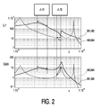
- the frequency-dependent transmission behavior of the resonance circuits in normal operating mode is shown in Figure 2 with solid lines.
- the gain is in the upper diagram (vertical axis) of the first resonant circuit, which is the output DC voltage U1 generates, depending on the frequency f (horizontal axis) of the other Nodes K1 and K2 fed AC voltage shown. Accordingly, in lower diagram the gain of the second resonant circuit, which is used to generate the DC output voltage Usb is used depending on the frequency of the input voltage shown.
- the frequency ranges Df1 and Df2 are shown in the diagrams, in which the DC-DC converter is preferably operated. It can be seen that the first DC output voltage U1 in the first frequency range Df1 is much larger than in the second Frequency range Df2.
- the second DC output voltage Usb is in both Frequency ranges Df1 and Df2 approximately the same size and in comparison smaller than the first DC output voltage U1.
- the first DC output voltage U1 can thus operate in both frequency ranges Df1 and Df2 with the second DC output voltage Usb remaining approximately the same, switched on and off become.
- the second frequency range Df2 therefore corresponds to a typical use the converter to the stand-by mode of a device operated with it.
- the function of the auxiliary switching elements M3 and M4 of the circuit according to FIG. 1 has not yet been discussed.
- the auxiliary switching elements M3 and M4 which form a half-bridge circuit and are in series, serve to implement an auxiliary circuit stage which is connected in parallel with the main circuit stage (switching elements M1 and M2) to the DC input voltage V dc .
- the auxiliary switching elements M3 and M4 are designed to be weaker in terms of the load absorption than the switching elements M1 and M2 of the main circuit stage and can therefore be embodied together with the control circuit C on a common chip 1.
- the midpoint between the two auxiliary switching elements M3 and M4 is over a Inductor L2 connected to the node K1. Additionally or alternatively to Inductance L2 can also be preceded by further turns of the transformer T.
- the other connection of the auxiliary switching element M3 is with the other node K2 (and one pole of the input voltage source). With the auxiliary circuit level off
- the hill switching elements M3 and M4 can be on the input side of the DC-DC converter a power saving in stand-by mode, in which a low output on the output side is removed, can be achieved.
- the main circuit stage M1, M2 deactivated by the control circuit C. both switching elements M1 and M2 are opened, and instead the auxiliary circuit stage M3, M4 controlled. Due to the different dimensions of the switching elements M3 and M4 as well as the interposed inductor L2 are created differently Transmission behavior of the converter, which is optimized for the required working point can be.
- control circuit C When the control circuit C is switched over to the standby mode, it opens the main circuit stage (M1, M2) and controls the auxiliary circuit stage (M3, M4) instead a frequency from the range Df2. Find the associated DC output voltages in the diagrams of Figure 2 on the dashed curve leading to the auxiliary circuit stage heard again. They are again identified by double arrows in the frequency range Df2, it can be seen that the DC output voltage U1 is very much lower than in normal operating mode, and that the output DC voltage Usb is approximately the same size as in normal operating mode.
- the inductance L2 can be integrated in the transformer T, it being additionally possible in the stand-by mode to change the winding N1 Current flow in stand-by mode is so small that the half-bridge of M3 and M4 is open the chip of the control circuit C can be integrated.
- the resonance of the second resonance circuit for the output voltage Usb can be lower Have goodness, which increases the possible control range in stand-by mode.
- the Voltage Usb can therefore be set precisely.
- the drive power required (for the gate charges) is minimal.
- a reduction of the current by a factor of 4.5 enables the use of field effect transistors for M3 and M4 with a 20-fold resistance (4.5 2 ). These have about a 20th of the input capacity. Accordingly, the power required for control is only a twentieth and remains at minimum values ( ⁇ 20 mW) even at high frequencies.
- the stand-by consumption of the circuit can be reduced from the current 3 W to 1 W at reduced costs.
- half-bridge circuit consisting of M1 and M2 can also be used for full-bridge circuits for the main circuit stage.
- Three half bridges are used (two large ones for the main circuit stage and an auxiliary bridge), and the various input voltages are regulated via the frequency.
Applications Claiming Priority (2)
| Application Number | Priority Date | Filing Date | Title |
|---|---|---|---|
| DE10118040 | 2001-04-11 | ||
| DE10118040A DE10118040A1 (de) | 2001-04-11 | 2001-04-11 | DC-DC Konverter |
Publications (2)
| Publication Number | Publication Date |
|---|---|
| EP1249925A2 true EP1249925A2 (fr) | 2002-10-16 |
| EP1249925A3 EP1249925A3 (fr) | 2004-01-07 |
Family
ID=7681200
Family Applications (1)
| Application Number | Title | Priority Date | Filing Date |
|---|---|---|---|
| EP02100359A Withdrawn EP1249925A3 (fr) | 2001-04-11 | 2002-04-10 | Convertisseur courant continu - courant continu |
Country Status (4)
| Country | Link |
|---|---|
| US (1) | US6587359B2 (fr) |
| EP (1) | EP1249925A3 (fr) |
| JP (1) | JP2002330583A (fr) |
| DE (1) | DE10118040A1 (fr) |
Cited By (1)
| Publication number | Priority date | Publication date | Assignee | Title |
|---|---|---|---|---|
| WO2019137681A1 (fr) * | 2018-01-12 | 2019-07-18 | Robert Bosch Gmbh | Convertisseur continu-continu et procédé pour faire fonctionner un convertisseur continu-continu |
Families Citing this family (15)
| Publication number | Priority date | Publication date | Assignee | Title |
|---|---|---|---|---|
| EP1287608A1 (fr) * | 2000-04-03 | 2003-03-05 | Aalborg University | Convertisseur auto-oscillant |
| SE523486C2 (sv) * | 2001-07-16 | 2004-04-20 | Abb Ab | Strömriktare samt förfarande för styrning av en strömriktare |
| DE10137676B4 (de) * | 2001-08-01 | 2007-08-23 | Infineon Technologies Ag | ZVS-Brückenschaltung zum entlasteten Schalten |
| EP1303032A3 (fr) * | 2001-09-04 | 2005-02-09 | Philips Intellectual Property & Standards GmbH | Dispositif de commande pour un convertisseur résonnant |
| JP2004215376A (ja) * | 2002-12-27 | 2004-07-29 | Sony Corp | スイッチング電源回路 |
| JP4984569B2 (ja) * | 2005-03-18 | 2012-07-25 | 富士通株式会社 | スイッチングコンバータ |
| CN101278468B (zh) * | 2005-10-03 | 2010-09-29 | 三垦电气株式会社 | 多输出开关电源装置 |
| JP4714250B2 (ja) * | 2008-09-10 | 2011-06-29 | 株式会社日立製作所 | Dc−dcコンバータ |
| GB2475518A (en) * | 2009-11-20 | 2011-05-25 | Technelec Ltd | Two stage resonant converter for LED lamps |
| US8363427B2 (en) * | 2010-06-25 | 2013-01-29 | Greecon Technologies Ltd. | Bi-directional power converter with regulated output and soft switching |
| US9515562B2 (en) * | 2013-03-05 | 2016-12-06 | Futurewei Technologies, Inc. | LLC resonant converters |
| US9190911B2 (en) * | 2013-03-05 | 2015-11-17 | Futurewei Technologies, Inc. | Auxiliary resonant apparatus for LLC converters |
| US9703313B2 (en) * | 2014-10-20 | 2017-07-11 | Ambiq Micro, Inc. | Peripheral clock management |
| KR101622139B1 (ko) | 2014-12-23 | 2016-05-19 | 한국에너지기술연구원 | 풀브리지 컨버터와 llc 컨버터의 출력이 직렬 결합된 컨버터 |
| US9602011B1 (en) * | 2015-12-28 | 2017-03-21 | Harman International Industries, Incorporated | Gated bi-directional dual-rail series resonant converter power supply |
Citations (4)
| Publication number | Priority date | Publication date | Assignee | Title |
|---|---|---|---|---|
| US5053937A (en) * | 1989-10-12 | 1991-10-01 | Siemens Aktiengesellschaft | Method for controlling push-pull series-resonant converter switching power supplies with regulated output voltage |
| US5777859A (en) * | 1995-08-16 | 1998-07-07 | U.S. Philips Corporation | Voltage converter |
| WO1999016163A2 (fr) * | 1997-09-22 | 1999-04-01 | Deutsche Thomson-Brandt Gmbh | Alimentation en puissance a mode commute |
| US6009005A (en) * | 1997-12-01 | 1999-12-28 | Samsung Electronics Co., Ltd. | Power supply device with reference signal generating circuit for power saving mode |
Family Cites Families (3)
| Publication number | Priority date | Publication date | Assignee | Title |
|---|---|---|---|---|
| JP2001359279A (ja) * | 2000-06-12 | 2001-12-26 | Sony Corp | ブリッジ型dc−dcコンバータ |
| US6246599B1 (en) * | 2000-08-25 | 2001-06-12 | Delta Electronics, Inc. | Constant frequency resonant inverters with a pair of resonant inductors |
| TW540197B (en) * | 2000-11-30 | 2003-07-01 | Delta Electronics Inc | Multi-function integrated DC converter |
-
2001
- 2001-04-11 DE DE10118040A patent/DE10118040A1/de not_active Withdrawn
-
2002
- 2002-04-09 US US10/118,871 patent/US6587359B2/en not_active Expired - Fee Related
- 2002-04-10 EP EP02100359A patent/EP1249925A3/fr not_active Withdrawn
- 2002-04-10 JP JP2002108220A patent/JP2002330583A/ja not_active Withdrawn
Patent Citations (4)
| Publication number | Priority date | Publication date | Assignee | Title |
|---|---|---|---|---|
| US5053937A (en) * | 1989-10-12 | 1991-10-01 | Siemens Aktiengesellschaft | Method for controlling push-pull series-resonant converter switching power supplies with regulated output voltage |
| US5777859A (en) * | 1995-08-16 | 1998-07-07 | U.S. Philips Corporation | Voltage converter |
| WO1999016163A2 (fr) * | 1997-09-22 | 1999-04-01 | Deutsche Thomson-Brandt Gmbh | Alimentation en puissance a mode commute |
| US6009005A (en) * | 1997-12-01 | 1999-12-28 | Samsung Electronics Co., Ltd. | Power supply device with reference signal generating circuit for power saving mode |
Cited By (1)
| Publication number | Priority date | Publication date | Assignee | Title |
|---|---|---|---|---|
| WO2019137681A1 (fr) * | 2018-01-12 | 2019-07-18 | Robert Bosch Gmbh | Convertisseur continu-continu et procédé pour faire fonctionner un convertisseur continu-continu |
Also Published As
| Publication number | Publication date |
|---|---|
| EP1249925A3 (fr) | 2004-01-07 |
| JP2002330583A (ja) | 2002-11-15 |
| US20020176264A1 (en) | 2002-11-28 |
| US6587359B2 (en) | 2003-07-01 |
| DE10118040A1 (de) | 2002-10-17 |
Similar Documents
| Publication | Publication Date | Title |
|---|---|---|
| EP1152519B1 (fr) | Convertisseur courant continu - courant continu | |
| DE3111776C2 (de) | Stereoverstärkeranlage | |
| EP1249925A2 (fr) | Convertisseur courant continu - courant continu | |
| EP0758815B1 (fr) | Convertisseur de tension | |
| EP1710898B1 (fr) | Convertisseur de tension commutable | |
| DE10122534A1 (de) | Resonanter Konverter | |
| DE202013102618U1 (de) | Netzteil, insbesondere Weitbereichsnetzteil | |
| WO2006106040A1 (fr) | Procede de fonctionnement d'une alimentation a decoupage avec recuperation d'energie de diffusion cote primaire | |
| EP0963032A1 (fr) | Convertisseur de courant alternatif en courant continu | |
| EP1438784B1 (fr) | Circuit redresseur synchrone | |
| EP1276218A2 (fr) | Dispositif circuit électrique | |
| EP1658676B1 (fr) | Circuit et procede pour transformer une tension d'alimentation a pics de tension | |
| DE102011005446A1 (de) | Schaltungsanordnung mit Wechselrichter zur Spannungsversorgung einer Röntgenröhre und zugehöriges Verfahren | |
| DE10334338A1 (de) | Gesteuerter Synchrongleichrichter zum Regeln einer Ausgangsspannung eines Schaltnetzteils | |
| DE4118918A1 (de) | Gleichspannungswandler | |
| EP1532726B1 (fr) | Regulateur a decoupage | |
| DE4036062C2 (de) | Netzteil mit geregelter Ausgangsspannung | |
| DE10135599A1 (de) | Schaltnetzteil mit Powerfaktorkorrektur, sowie Spule für eine diesbezügliche Korrekturschaltung | |
| DE4418780A1 (de) | Gleichspannungskonverter | |
| DE102004035248B4 (de) | Resonanzwandler | |
| EP0648007A1 (fr) | Agencement de circuit pour limiter la tension de sortie d'un régulateur de tension par découpage | |
| EP0263936A1 (fr) | Alimentation de puissance à commutation sur le circuit secondaire | |
| DE102017109541B4 (de) | Umschalter, Spannungsversorgung und Antriebssytem | |
| EP1174991A2 (fr) | Convertisseur | |
| WO2022028754A1 (fr) | Convertisseur de puissance avec filtre de mode commun |
Legal Events
| Date | Code | Title | Description |
|---|---|---|---|
| PUAI | Public reference made under article 153(3) epc to a published international application that has entered the european phase |
Free format text: ORIGINAL CODE: 0009012 |
|
| AK | Designated contracting states |
Kind code of ref document: A2 Designated state(s): AT BE CH CY DE DK ES FI FR GB GR IE IT LI LU MC NL PT SE TR |
|
| AX | Request for extension of the european patent |
Free format text: AL;LT;LV;MK;RO;SI |
|
| RAP1 | Party data changed (applicant data changed or rights of an application transferred) |
Owner name: KONINKLIJKE PHILIPS ELECTRONICS N.V. Owner name: PHILIPS INTELLECTUAL PROPERTY & STANDARDS GMBH |
|
| PUAL | Search report despatched |
Free format text: ORIGINAL CODE: 0009013 |
|
| AK | Designated contracting states |
Kind code of ref document: A3 Designated state(s): AT BE CH CY DE DK ES FI FR GB GR IE IT LI LU MC NL PT SE TR |
|
| AX | Request for extension of the european patent |
Extension state: AL LT LV MK RO SI |
|
| RIC1 | Information provided on ipc code assigned before grant |
Ipc: 7H 02M 3/337 B Ipc: 7H 02M 3/335 A |
|
| 17P | Request for examination filed |
Effective date: 20040707 |
|
| RAP1 | Party data changed (applicant data changed or rights of an application transferred) |
Owner name: KONINKLIJKE PHILIPS ELECTRONICS N.V. Owner name: PHILIPS INTELLECTUAL PROPERTY & STANDARDS GMBH |
|
| AKX | Designation fees paid |
Designated state(s): AT BE CH CY DE DK ES FI FR GB GR IE IT LI LU MC NL PT SE TR |
|
| STAA | Information on the status of an ep patent application or granted ep patent |
Free format text: STATUS: THE APPLICATION HAS BEEN WITHDRAWN |
|
| 18W | Application withdrawn |
Effective date: 20051103 |
|
| RAP1 | Party data changed (applicant data changed or rights of an application transferred) |
Owner name: KONINKLIJKE PHILIPS ELECTRONICS N.V. Owner name: PHILIPS INTELLECTUAL PROPERTY & STANDARDS GMBH |